

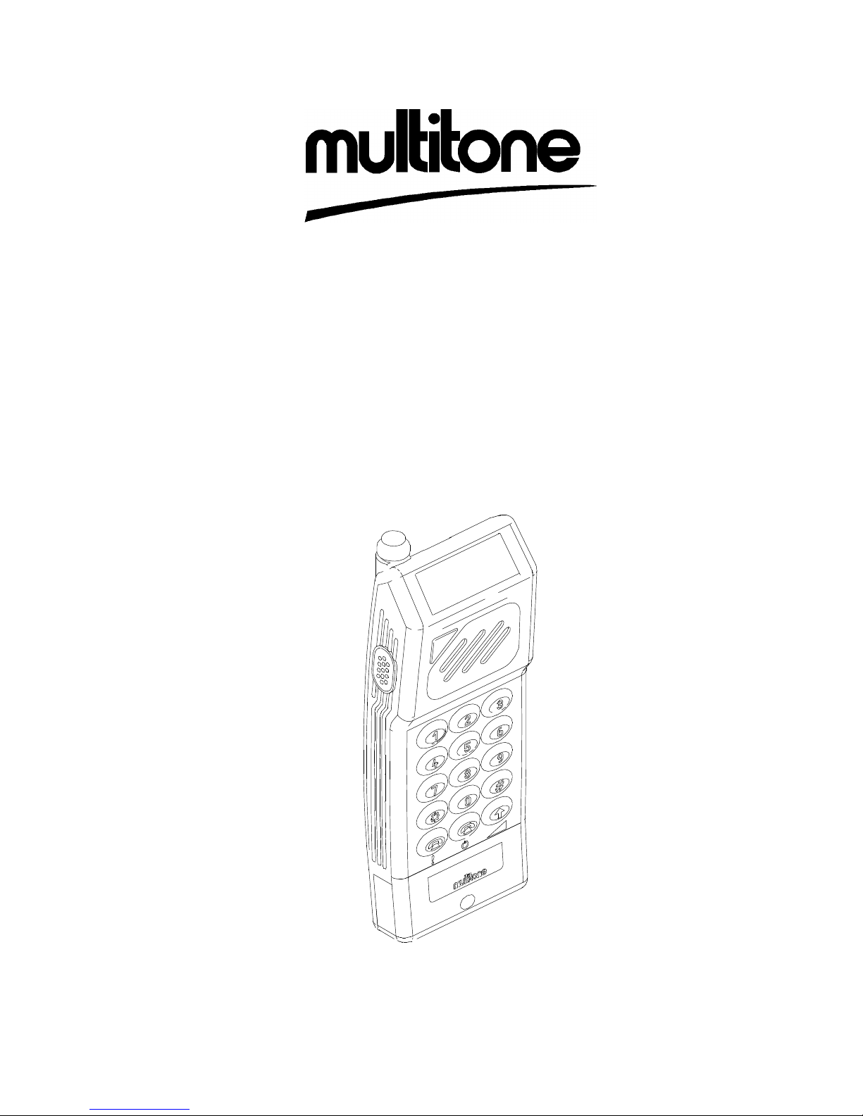
RPR 563GS/KGS
TM1187A Issue C Page (i)
TECHNICAL MANUAL
for
RADIO TRANSCEIVER HANDSET
MODELS RPR 563GS and RPR 563KGS
Printed and Published in England

RPR 563GS/KGS
TM1187A Issue CPage (ii)
COMPANY LIABILITY
The information in this manual has been carefully compiled and checked for technical
accuracy. Multitone Electronics plc accept no liability for inaccuracies or errors. In line with
the company policy of technical advancement, the information within this document may be
changed. The user should ensure that the correct issue of the document is used. Comments
or correspondence regarding this manual should be addressed to:
Multitone Electronics plc
Marketing Communications
Kimbell Road
Basingstoke
Hampshire
RG22 4AD
England
ISSUE DATE
C March 1998
© Multitone Electronics plc 1998

RPR 563GS/KGS
TM1187A Issue C Page (iii)
CONTENTS
Page (i) Title Page
Page (ii) Company Liability
Page (iii) Contents
Page (iv) Effective Page List
Page (v) Safety Summary
Warning
Page (vi) Caution
Section 1 Introduction and Specification
Section 2 Operating Instructions
Section 3 Technical Description
Section 4 Installation & Commissioning
Section 5 Servicing
Section 6 Spare Parts List
Section 7 Diagrams

RPR 563GS/KGS
TM1187A Issue CPage (iv)
EFFECTIVE PAGE LIST
Page No. Issue Page No. Issue Page No. Issue Page No. Issue
(I) C 2-13 C 5-9 C 5C-1 C
(ii) C 2-14 C 5-10 C 5C-2 C
(iii) C 2A-1 C 5-11 C 6-1 C
(iv) C 2A-2 C 5-12 C 6-2 C
(v) C 2A-3 C 5-13 C 6-3 C
(vi) C 2A-4 C 5-14 C 6-4 C
1-1 C 3-1 C 5-15 C 6-5 C
1-2 C 3-2 C 5-16 C 6-6 C
1-3 C 3-3 C 5-17 C 6-7 C
1-4 C 3-4 C 5-18 C 6-8 C
1-5 C 3-5 C 5-19 C 6-9 C
1-6 C 3-6 C 5-20 C 6-10 C
1-7 C 3-7 C 5-21 C 7-1 C
1-8 C 3-8 C 5-22 C 7-2 C
1-9 C 3-9 C 5-23 C 7-3/4 C
1-10 C 3-10 C 5-24 C 7-5/6 C
2-1 C 3-11 C 5-25 C 7-7/8 C
2-2 C 3-12 C 5-26 C 7-9/10 C
2-3 C 4-1 C 5-27 C 7-11/12 C
2-4 C 4-2 C 5-28 C 7-13/14 C
2-5 C 5-1 C 5-29 C 7-15/16 C
2-6 C 5-2 C 5-30 C 7-17/18 C
2-7 C 5-3 C 5A-1 C 7-19/20 C
2-8 C 5-4 C 5A-2 C 7-21/7-22 C
2-9 C 5-5 C 5B-1 C 7-23/7-24 C
2-10 C 5-6 C 5B-2 C 7-25 C
2-11 C 5-7 C
2-12 C 5-8 C
RPR 563GS/KGS
TM1187A Issue C Page (v)
THE TRANSCEIVER SHOULD NOT BE CARRIED INTO AREAS WHERE EXPLOSIVE
GASES MAY BE PRESENT.
SAFETY SUMMARY
The following information applies to both operating and servicing personnel. General
Warnings and Cautions will be found throughout the manual, where they apply, which refer
to the applicable part of this summary.
WARNING statements identify conditions or practices that could result in personal injury or
loss of life.
CAUTION statements identify conditions or practices that could result in equipment damage.
WARNING

RPR 563GS/KGS
TM1187A Issue CPage (vi)
CAUTION
STATIC SENSITIVE DEVICES ARE USED WITHIN THIS EQUIPMENT. CARE MUST BE
USED TO ENSURE DAMAGE TO THESE DEVICES IS NOT CAUSED BY HIGH LEVELS
OF STATIC ELECTRICITY. SPARE BOARDS OR COMPONENTS SHOULD BE STORED
IN ANTI-STATIC PACKAGING WHEN NOT INSTALLED IN THE EQUIPMENT.
PROTECT THE TRANSCEIVER FROM LIQUIDS, STRONG MAGNETIC FIELDS AND
EXTREME TEMPERATURES. DO NOT LEAVE THE TRANSCEIVER EXPOSED TO
STRONG SUNLIGHT. AREAS SUCH AS WINDOW LEDGES ARE TO BE AVOIDED.

RPR 563GS/KGS
Page 1 - 1TM1187A Issue C
SECTION 1
INTRODUCTION & SPECIFICATION
CONTENTS:
1. ROLE
STANDARD FEATURES
6. Liquid Crystal Display (LCD)
7. Acoustic and Visual Alerts
8. Message Storage
9. Message Length
10. Beep Code Alpha
11. Automatic Speech Switching
12. Battery Economy Circuit (BEC)
13. Display Direction Control
14. Engineering Program Mode
OPTIONAL FEATURES
15. Permanent On
16. Alert Duration
17. Escalating Alert (Escalert)
18. Extended Alert
19. Group Call
20. Call Comparator
21. Time-of-Day
22. Mute Mode
23. Program Volume Levels
24. Battery Low Indication
25. Display Direction at Switch-On
26. Speech Timeout
27. Address Digits Displayed
28. Test Mode
29. System Number
30. System Retry Interval
31. Line Service (RPR 563GS only)
32. Switch-On and Rack Message
SPECIFICATION
33. Receiver
34. Transmitter
35. Signalling Formats
36. Power Supplies
37. Controls, Indicators, Alerts
38. Physical Characteristics

RPR 563GS/KGS
Page 1 - 2 TM1187A Issue C
TABLE Page
1. DTMF Frequency Pairs 1 - 9
2. Battery Life 1 - 9
ROLE
1. The Multitone RPR 563KGS is a UHF FM transceiver with selective calling and two-way
speech facilities. The unit can receive alphanumeric messages and can make selective
calling, speech and telephone calls. A sub-audio tone encoder/decoder is incorporated
ensuring that unwanted transmissions are ignored. The transceiver may be used in
simplex or duplex (telephone-style) mode.
2. Selective calling and telephone calls are made via a DTMF keypad. A reduced keypad
version of the transceiver, designated the RPR 563GS, (which does not have a DTMF
keypad) is available which is able to make limited telephone-style calls.
3. The transceiver is powered from a plug-in nickel-cadmium or metal hydride battery pack
which may be trickle or fast-charged via contacts in the base. Another set of contacts
in the battery pack allow the transceiver to be programmed, and allow absence
registration when used with absence/charging racks on Multitone systems.
4. Selective calls to the receiver are in Multitone Mk7 digital format which has a capacity
of up to 10,000 individual address codes. Visual alert is by flashing LED and eight
audible tone alert patterns (Beep Code) are available. Alphanumeric messages can be
displayed on a 14-character dot matrix Liquid Crystal Display (LCD).
5. The unit is housed in a Bayblend case which provides a lightweight but strong
construction. A pocket clip, holster and wrist strap lanyard are available as carrying
devices.
STANDARD FEATURES
Liquid Crystal Display (LCD)
6. The LCD provides a visual display of up to 14 alphanumeric characters (longer
messages are displayed in 14 character blocks). A backlight provides enhanced LCD
viewing under low light conditions.
Acoustic and Visual Alerts
7. A range of eight different audible tone alert codes (beep codes) are programmed as
standard. These alerts, when initiated, are accompanied by the illumination of an LED
to provide visual indication of a call. Speech calls are indicated by ringing patterns
which match the appropriate tone alert codes.

RPR 563GS/KGS
Page 1 - 3TM1187A Issue C
Message Storage
8. Up to five messages may be stored by the transceiver for review later. They are held
on a first in/first out basis.
Message Length
9. The maximum length of any received message is between 63 and 81 characters,
depending on whether beep code alpha and time stamp are in use.
Beep Code Alpha
10. Up to four beep codes may be reserved to trigger an associated alphanumeric message;
each message not exceeding 14 characters in length.
Automatic Speech Switching
11. Allows speech to follow automatically after an alert tone.
Battery Economy Circuit (BEC)
12. The radio channel is monitored periodically and when no activity is present the receiver
circuits are powered down, hence conserving energy and battery life.
Display Direction Control
13. The direction of the display may be changed to suit the way in which the transceiver is
carried.
Engineering Program Mode
14. May be used for reviewing programmed options in the transceiver. This feature is useful
for when carrying out engineering work on the system.

RPR 563GS/KGS
Page 1 - 4 TM1187A Issue C
OPTIONAL FEATURES
Permanent On
15. When a battery pack is fitted and the Permanent On option enabled, the transceiver
cannot be switched off.
Alert Duration
16. This is the duration of the alert tone at normal volume level. Options are 8s, 16s, 32s,
or continuous alert. This does not include the period of any `Silent' and/or `Quiet'
beep(s) that may be programmed. When a speech call is received, the programmed
option is overridden and the alert duration is reduced to 4s.
Escalating Alert (Escalert)
17. Defines the alert sequence, which is four seconds of silence (LED only), followed by four
seconds of Quiet beep, and the remainder of the alert as Full beep.
Extended Alert
18. Extended Alert is an additional alert sequence which acts as a reminder if the original
alert is not acknowledged. During Extended Alert, the LED flashes every two seconds,
and every two minutes two pips are emitted unless the transceiver is in Mute Mode.
Group Call
19. Group Call is an option which allows the receiver to be alerted as part of a group (or
team). If enabled, any call to the group will alert the user audibly. The Group size may
be none, 10 or 100 as required.
Call Comparator
20. Prevents the transceiver from reacting to an identical message received within a predetermined period. Options are none, 30s, 120s, 300s or disabled.
Time-of-Day
21. When enabled, displays the time in hh:mm format. The transceiver uses an internal
clock which is synchronised by time information from the last valid Mk7 call.

RPR 563GS/KGS
Page 1 - 5TM1187A Issue C
Mute Mode
22. When Mute Mode is enabled, tone alert is suppressed when calls are received.
However, if a mute override beep code is received (triple pip or continuous pips), mute
is ignored and the transceiver responds with audible and visual alerts.
Program Volume Levels
23. On RPR 563KGS transceivers, the volume levels for beep tone, ring tone, telephone
speech, simplex speech and DTMF echo may be adjusted from the keypad.
Battery Low Indication
24. Visual and audible indication of low battery voltage indication are available as
programmable options.
Display Direction at Switch-On
25. Display direction may be changed for handheld or belt-worn operation. When the
transceiver is switched off, the current display direction is stored in EEPROM, unless the
battery is low. The default display direction is correct for handheld operation.
Speech Timeout
26. The speech timeout duration may be set for 10s, 30s, 300s, or continuous. The default
is 300s.
Address Digits Displayed
27. At switch-on, the number of address digits displayed is programmable between two and
five digits. The default is five digits.
Test Mode
28. This is for engineering use only. This feature limits the beep duration to one second and
defeats the call comparator.
System Number
29. The System Number for the Mk7 Digital format may be set to 0, 1, 2, or 3. The default
system number is 1.

RPR 563GS/KGS
Page 1 - 6 TM1187A Issue C
System Retry Interval
30. The System Retry Interval may be set to 30s, 45s, 60s or 90s. The default is 30s.
Line Service (RPR 563GS only)
31. The following Line Service options may be specified, call to a telephone extension,
broadcast to all Manual Control Units (MCUs), broadcast to specific MCU (1-9), teams,
and users. The default option is Broadcast to all MCUs.
Switch-On and Rack Message
32. A Switch-On message of up to 14 characters may be programmed. A Rack Message
of up nine characters, which is displayed when the transceiver is inserted into an
absence rack, may also be programmed. The default Switch-On message is
"Multitone 560" and the default Rack message is "Absent".

RPR 563GS/KGS
Page 1 - 7TM1187A Issue C
SPECIFICATION
Receiver
33. The following parameters apply to the receiver section of the transceiver:
a) Frequency Range: 440.025MHz to 441.000MHz
b) Number of Channels: 1
c) Channel Spacing: 25kHz.
d) Intermediate Frequencies: 21.4MHz and 455kHz.
e) Crystal Frequencies:
1st oscillator (XL303) carrier frequency + 21.4MHz
9
2nd oscillator (XL302) 20.945MHz
f) Sensitivity (TEM Cell): -88dBm (-95dBm typical) TEM Cell
(6dB degradation allowed at extremes of
operating temperature range).
g) Sensitivity (On-Body): 50µV/m (25µV/m typical) 8-position
h) Adjacent Channel Selectivity: Better than 50dB (60dB typical)
i) Co-Channel Rejection -12dB (-5dB typical)
j) Spurious Response 45dB (55dB typical)
k) Intermodulation Response: 45dB (55dB typical) 2-signal method.

RPR 563GS/KGS
Page 1 - 8 TM1187A Issue C
Transmitter
34. The following parameters apply to the transmitter section of the transceiver:
a) Frequencies: 448.125MHz to 449.000MHz.
b) Number of Channels: 1
c) Channel Spacing: 25kHz.
d) Crystal Frequency: carrier frequency (MHz)
18
e) Frequency Stability: ±2.5kHz.
f) Output Power: #50mW (conducted). (3dB degradation
allowed at extremes of operating
temperature range.)
g) Radiated Output Power 15-50mW (40mW typical).
h) Adjacent Channel Power: 0.2µW at ±20kHz.
i) Antenna: Telescopic (standard)
Flexible (optional).
j) Deviation: ±4.0kHz.
k) Spurious Radiation: 0.25µW max (30-1000MHz)
1.0µW max (1.0-12.75GHz)
Spurious radiation is better than 4nW at
the following frequencies: 41-68MHz, 87.5-
118MHz, 162-230MHz, 470-862MHz &
10.7-12.75GHz.
Signalling Formats
35. The transceiver signalling parameters are as follows:
a) Tone Squelch Frequencies: 88.5, 103.5, 114.8, 127.3, 141.3Hz
b) Selective calling Code Format: Multitone Mk7 digital format (Manchester
encoded).
c) DTMF Frequency Pairs: see Table 1.

RPR 563GS/KGS
Page 1 - 9TM1187A Issue C
TONE FREQUENCY
PAIRING
HIGH FREQUENCY GROUP (Hz)
1209 1336 1477 1633
LOW
FREQUENCY
GROUP (Hz)
697
1 2 3 A
770
4 5 6 B
852
7 8 9 C
941
* 0 # D
Table 1: DTMF Frequency Pairs
BATTERY
PACK
STANDBY
(NO TRAFFIC AND
CONTINUOUS ON)
USEAGE
PROFILE MODEL
(Tx TIME)
P566 120 HOURS 1 HOUR IN
12 HOUR SHIFT
P565 240 HOURS 2 HOURS IN
12 HOUR SHIFT
Table 2: Battery Life
Power Supplies
36. The following battery packs are available for powering the transceiver:
a) Battery Type:
(i) Battery Pack P566: 3.6V (nominal) 600mAH Metal-Hydride re-
chargeable pack.
(ii) Battery Pack P565: 3.6V (nominal) 1200mAH Metal-Hydride
re-chargeable pack.
b) Battery Life (P565) (typical):
Controls, Indicators, Alerts
37. The following controls, indicators and alerts are available:
a) Controls: Keypad (15 keys on RPR563KGS, 3 keys
on RPR563GS).
Press-to-Talk button.
On/Cancel button.

RPR 563GS/KGS
Page 1 - 10 TM1187A Issue C
b) Indicators: 14 character (7 x 5 dot matrix) Liquid
Crystal Display (LCD) with icon. Viewing
area 33.1mm x 5.8mm.
Alert LED (red).
Transmit LED (green).
Keyboard backlight.
c) Audible Alert 78dB (82dB typical) SPL @ 30cm (full
volume).
Physical Characteristics
38. The following parameters apply to the physical characteristics of the transceiver:
a) Temperature Range: -10EC to +55EC (Operational)
(LCD performance may be degraded below
0EC and above +45EC).
-20EC to +70EC (Storage)
b) Environmental: Designed to meet IP52
c) Dimensions: Length: 159mm
Width: 58mm
Depth: 21mm
(with 600mAH battery pack).
d) Weight: #269gm with 1200mAH Battery Pack
e) Case Material: Bayblend in Storm Grey.

RPR 563GS/KGS
TM1187A Issue C Page 2 - 1
SECTION 2
OPERATING INSTRUCTIONS
CONTENTS:
1. CONTROLS AND INDICATORS
OPERATION
5. Fi tting the Battery Pack
7. Switching On
9. Quiescent Mode
10. Receiving a Non-Speech Call
17. Receiving a Speech Call (Selective Calling)
21. Receiving a Speech Call (Telephone Style)
23. Loud Speech (Simplex)
25. New Status
26. Cancell ing Alerts
27. Escalati ng Alert
29. Extended Alert
30. Memory Replay
34. Making a Call (Telephone-Style Operation)
38. Making a Call to a Telephone (RPR 563KGS only)
39. Making a Call to Another Mobile (RPR 563KGS only)
42. Making a Call to a Manual Control Unit (RPR 563KGS only)
43. Terminating a Call
47. Program Volume Modes
49. ABSENCE RACK REGISTRATION AND CHARGING
55. RECHARGING THE BATTERY PACK
TABLES Page
1. Message Display Formats 2 - 6
2. Beep Code and Alert Patterns 2 - 9
FIGURES
1. RPR563GS/KGS Transceiver 2 - 2
2 DTMF Keypad and Function Keys 2 - 3
3. Fitting the Battery Pack 2 - 4
4. Switch On Sequence 2 - 5
ANNEXE
A Engineering Mode
1
3
4
5
6
7
8
9
10
12
11
13
14
PSG10150-1
2
RPR 563GS/KGS
TM1187A Issue CPage 2 - 2
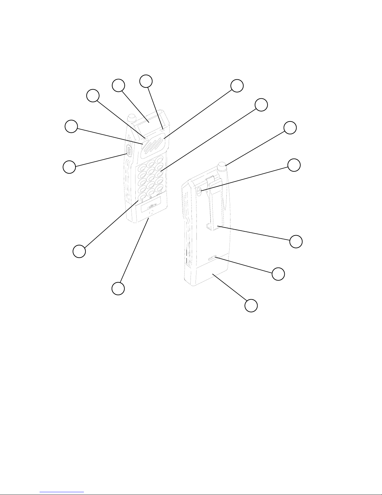
KEY:
1. Microphone
2. Function Keys
3. Press-to-Talk Butto n
4. Cancel/On/Memory Button
5. Alert LED
6. Liquid Crystal Dis play
7. Tx LED
8. Loudspeaker
9. DTMF Keypad (RPR563KGS only)
10. Antenna
11. Wrist Strap Loop
12. Pocket Clip
13. Battery Pack Button
14. Battery Pack
Figure 1: RPR563GS/KGS Transceiver
CONTROLS AND INDICATORS
1. Controls and indicators for the transceiver are shown in Figure 2.

DTMF KEYPAD
(RPR563KGS ONLY)
FUNCTION KEYS
PSG10516-1
RPR 563GS/KGS
TM1187A Issue C Page 2 - 3
Figure 2: DTMF Keypad and Function Keys
2. The foll owing controls are found on both the full and reduced keypad versi ons of the
transceiver:
PRESS-TO- T ALK Us e d to manually key the transmitter on (selective calling
only).
ON/CANCEL/ Initially switches on the transceiver and then subsequently
MEMORY cancels incoming calls, or illuminates LCD and keypad
RECALL (when no calls received). Recalls stored messages.
LINE Press button to request a li ne before dia l li ng tel ephone or
selective calling code (or for direct connection on reduced
keypad option). Pressing button twice during a tel ephone
call puts the transceiver into loud speech mode. Press Shift
followed by for Emergency line request.
CLEAR/OFF/ Pre ssing during a speech call ends the cal l. Press
MUTE Shift key ( ) followed by to mute the transceiver.
Pres s Shift and hold down for three seconds to
switch off transceiver.
SHIFT/REVERSE P ress and hold to adj ust speech v olume ( ) during a call.
Used in conjunction with a second key initiates the
alternative function for that key. Pressed twice during
status interrogation reverses displ a y.
3. In addition to the controls in paragraph 2, the full keypad version also has keys `0' to
`9', `*' and `#'.
PSG10152-1
RPR 563GS/KGS
TM1187A Issue CPage 2 - 4
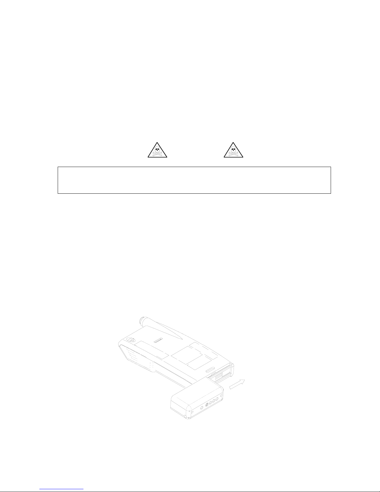
THE TRANSCEIVER SHOULD NOT BE CARRIED INTO AREAS WHERE EXPLOSIVE
CAUTION
PROTECT THE TRANSCEI VER FROM LIQUIDS, STRONG MAGNETIC F IELDS AND
EXT RE ME TEMPERATURES. DO NOT LEAVE T HE TRANSCEIVER EXPO SED TO
STRONG SUNLIGHT. AREAS SUCH AS WINDOW LEDGES ARE TO BE AVOIDED.
Figure 3: Fitting the Battery Pack
4. The transceiver has the following indicators:
a) LCD A 14-character alphanumeric display. This displays selective call
messages, and transceiver and system status messages.
b) Tx KEY Lights when the transmitter is active.
c) ALERT Lights when a selective call has been received.
OPERATION
WARNING
Fitting the Battery Pack
5. Refer to Figure 3. Hold the battery against the transceiver as shown in Figure 3. Slide
the battery pack onto the lower edge of the transceiver until it clicks into positi on.

RPR 563GS/KGS
TM1187A Issue C Page 2 - 5
Figure 4: Switch On Sequence
6. Re moval is a reversal of the above procedure, but press the battery button before
releasing the battery pack.
Switching On
7. Check that a fully-charged battery pack has been fitted. Press once. The
transceiver will initiate its switch on sequence as shown in Figure 4.
8. The address display will depend on the number of address digits option. When the
swit ch-on sequence has fi nished the transceiver enters the quiescent mode. If the
EEPROM is faulty, then a series of `E's will be displayed.
Quiescent Mode
9. This is the transceiver's normal operating state, when no calls are being made or being
rec ei ve d, no buttons are pressed and the backl ights are off. The displ ay shows the
highest priority status, and, if enabled, Time-of-Day information (hh:mm) derived from
the transceiver's internal clock..
Receiving a Non-Speech Call
10. When a call is received, the Alert LED will flash and, optionally, a series of beeps will
be heard. Press to cancel the alert and read the accompanying message.

RPR 563GS/KGS
TM1187A Issue CPage 2 - 6
Table 1: Message Display Formats
11. The displayed message comprises combinations of the foll o wing elements:
Element Example
a) Time stamp + space 12:00
b) Beep Code (Tone Only message) 4
c) Speech call Call ended
d) Beep code alpha Fire
e) Off-Air Message (Alpha) Please call reception
f) Message Terminator ** or **?
12. Unless in test mode, all messages are in one of the formats shown in Table 1.
13. The terminator **? is used when the call contains any suspect characters, or is
terminated early because of corrupt data. Otherwise the terminator ** is used.
14. When the total message length is 14 characters or less, it is displayed for the duration
of the aler t, if uncancelled. On cancel ling the alert the message is displayed for a
further 2.5 seconds.
15. When the total message length is greater than 14 characters, it scrolls through to the
end of the message at 1.25 second intervals, pausing for 2.5 seconds on the final
screen. This process continues until the alert is cancelled. On ca nce lling the alert the
message is displayed again from the beginning.

RPR 563GS/KGS
TM1187A Issue C Page 2 - 7
16. The tra nsce iv er is a b le t o rece i v e n e w ca lls duri n g a n a l e r t , a lthough receiver sensitivity
may be degraded. The new call takes over the previous call, which is placed in
memory. Preceding calls have "new" status unless cancelled during the alert.
Receiving a Speech Call (Selective Calling)
17. When a call is received, the Alert LED will flash and a telephone-style ringing tone will
be audible for four seconds. On receipt of sub-audio tone from the system the
transceiver will switch into speech mode. The message will be displayed as for a nonspeech call. If the sub-audio tone is present, the speech audio channel switches on
immediately after the alert.
18. Press to cancel the alert and wait to hear the speech message. A further press of
the button cancels speech. If is pressed again, before the speech timeout period
expires, the speech channel may be re-opened.
19. The call is terminated by one of the following actions:
a) pressing
b) pressing
c) expiration of the transceiver speech timeout
d) a Mk7 speech termination signal from the system.
20. If the speech call has been rejected by two presses of , any subsequent pressing of
is assumed to be a new call request (see `Making a Call').
Receiving a Speech Call (Telephone Style)
21. Assuming a speech call has been received (as in paragraph 17) press to talk back.
The transceiver will be switched into telephone mode and the speech audio level wil l
dro p t o the programmed telephone speech level. The display di rection will be set to
read correctly for keyboard use. When the call ends, volume level and display direction
will return to their default settings. Extended alert and new status are cancelled.
22. The call is terminated by pressing , the speech timeout, or by a Mk7 speech
ter minat ion signal from the system. The transceiver will display the message "Call
ended".

RPR 563GS/KGS
TM1187A Issue CPage 2 - 8
Loud Speech (Simplex)
23. Under some circumstances telephone-style communication will not be possible, e.g.
noisy environment, wearing of protective headgear, etc. The high volume levels
required for listening would inhi bi t operation because of feedback. In this situation a
PMR-style of operation is desirable.
24. T o se lect loud speech, press twice (the message "Use PTT" is displayed). To
speak, depress the PTT key. Release the PTT switch after speaking, to listen to the
oth er party. Subsequent presses of toggles the transceiver between telephone
mode (the m essage "On" is displayed) and loud speech mode (message "Use PTT" is
displayed).
New Status
25. Each call is automatically given new status when first received. New status is removed
by cancelling the alert or reviewing the call from memory. If the alert is left uncancelled
then the prompt "x new messages" appears on the display showing the number of
messages with new status (where x is a integer from 1 to 5). Each message must be
viewed in full for new status to be removed.
Cancelling Alerts
26. Ca nce l t he alert by pressing the button. The beep and LED alert cease but the
message is replayed from the beginning.
Escalating Alert
27. The escalating alert has three stages - the first two lasting 4 seconds each and the last
one 8s, 16s, 32s or continuous. The stages are as follows:
Stage 1: LED, flashing beep pattern.
Stage 2: LED, low volume beep pattern.
Stage 3: LED, full volume beep pattern.
28. The option for Escalating Alert is programmed into the EEPROM. However, the
escalating alert and the Mute mode are overridden by beep code 5 (triple pip) and beep
code 8 (continuous pip). They cause the alert to be on full volume for the whole of the
programmed alert duration.
Continuous Beep
Single Be ep
Double Beep
Triple Be ep
Single Pip
Double Pip
Triple Pip
Continuous Pip
Silent Al ert
PIP/BEEP TONE ALERT PATTERN
4
1
3
2
6
7
5*
8*
9
BEEP CODE
RPR 563GS/KGS
TM1187A Issue C Page 2 - 9
Table 2: Beep Code and Alert Patterns
* The escalating alert and the Mute mode are overridden by beep code 5
(triple pi p) and beep code 8 (continuous pip). They cause the alert to be on
full volume for the whole of the programmed alert time, or for four seconds
if it is a speech call.
NOTE: Silent Alert is not currently supported by Access 3000 systems.
Extended Alert
29. If enabled and the c all is not cancelled, the transceiver enters extended alert after the
normal alert has finished. During extended alert, the LED flashes for 0.125s, every 2s.
Two 0.125s pips (2s apart) are emitted every two minutes (unless in Mute mode). The
pips are synchronised to the LED flashes.

RPR 563GS/KGS
TM1187A Issue CPage 2 - 10
Memory Replay
30. Incoming messages are automatically entered into the transceiver's mem ory store which
can accomm odate up to five calls. To start the memory replay cycle, from the quiescent
dis play, press the button twice. If in extended alert, press the key once only.
The transceiver displays the header of the first message (or the phrase "no messages"
if none exist). If no messages exist, the display returns to quiescent mode after
2 seconds.
31. Ne w messages which have not been cancelled are displayed first. W hen all new
messages have been reviewed, the tra nsceiver returns to qui escent mode. Once new
status has been removed it is possible to view all the messages in the memory by
pressing again.
32. The header refers to the fi rst message screen and consists of a time stamp, plus the
initial part of the message (or the whole message if 14 characters or less). Press
to step through each message header on the display. The most recent call is displayed
first and corresponds to the `1'.
33. The display automatically scrolls through messages at 1.25 second intervals until the
final screen is reached. The final screen terminates in ** (to denote the end of the
message) and is displayed for 2.5 seconds. If all messages have been viewed the
transceiver display returns to the quiescent condition.
Making a Call (Telephone-Style Operation)
34. The procedure for making a telephone-style call is as follows:
a) Press . The message "Please Wait" will be displayed. If the channel is clear
(base station not transmitting sub-audio tone) then the transcei ver sends its Talk
code in DTMF. The transceiver then reverts to its quiescent state.
b) W hen the system is ready to service the call it sends a "Line Ready" call. The
transceiver rings, displays the message "Ready" and drops into telephone mode,
i.e. the transceiver audio volume will be adjusted to telephone speech level. Dial
tones from the system will normally be heard on the RPR 563KGS version.
c) Enter the required di a lling sequence.
35. If, after a predetermined interval, the system does not respond with a "Line Ready" call,
the transceiver sends its Talk code again, and repeats thi s process at the specified
interval until a response is received from the system. If the key has been pressed
and a Line Ready call is subsequently received, the transceiver still sends the Un-Talk
code and reverts to its quiescent state.
36. The line request can be cancelled at any time by pressing .

RPR 563GS/KGS
TM1187A Issue C Page 2 - 11
37. On RPR 563GS (reduced keypad version), connection to the designated point is
automatic once has been pressed.
Making a Call to a Telephone (RPR 563KGS only)
38. Once the dial li ng tone has been recei ved, the telephone number may be dialled as if
calling from another telephone.
Making a Call to Another Mobile (RPR 563KGS only)
39. The procedure for making a call to another mobile is as detailed in paragraph 34. If the
call is to another receiver, then the user number and numeric message must be dialled
when requested by the system.
40. A control message is sent by the system which sets the transceiver into simplex mode.
If s u b - a u di o tone from the system is lost before the control message is received, the
transceiver displays the message "Please Wait". When the sub-audio tone re-appears,
the message "Use PTT" is displayed.
41. If the recipient has a non-speech receiver then the system clears down the originator
when the message has been sent.
Making a Call to a Manual Control Unit (RPR 563KGS only)
42. Once the "Line Ready" call has been received, connection is made using designated
MCU intercepts. The default intercept numbers are:
*0 to call several MCUs which have continuous talkback monitoring facilities
or:
*1 to *8 to call a designated MCU.
Terminating a Call
43. To terminate a call, press . The transceiver sends i ts Un-Talk code, displays the
message "Call ended" and reverts to quiescent state.
44. An internal speech timeout function will terminate a speech call if it has not been
terminated manually. The system may also terminate the call but will warn the user with
a tone a few seconds before termination.

RPR 563GS/KGS
TM1187A Issue CPage 2 - 12
45. If a team call is transmitted, or another user makes an emergency "Burst-In" call, the
system w ill override and terminate the call without prior warning. The transceiver that
has been overridden will display the message "Call Override".
46. If the battery pack voltage becomes too low during a transmission, the transceiver
sends the un-talk code at low volume and then keys down. A `low-battery' buzz is then
generated if the option is enabled.
Program Volume Modes
47. Pr ess in g f oll owed by [1], followed by a DTMF key between 1 and 5 initiates the
setting for one of five transceiver volume modes, as follows:
Key Sequence Function Displayed Message
[1] [1] Beep Tone Volume Volume 1:
[1] [2] Ring Volume Volume 2:
[1] [3] Simplex Speech Volume Volume 3:
[1] [4] Telephone Speech Volume Volume 4:
[1] [5] DTMF Volume Volume DTMF:
48. To reduce the volume level for the selected mode, press [ ] repeatedly until the correct
*
lev e l i s attai ned. To increase the vol ume level, press [#] repeatedl y until the correct
level is attained. To store the new setting, press [1]. The new setting is also stored if
no key presses are made for at least six seconds. On leaving this mode, the message
"Volume Set" is displayed.
ABSENCE RACK REGISTRATION AND CHARGING
49. T he tra nsceiver contains a rack message which may be up to a maximum of nine
characters in length. The factory programmed default rack message "Absent" may be
changed by using Programm ing Unit P648 and programming software P648T, together
with an IBM PC or compatible personal computer.
50. Insert the transceiver into a pocket within the rack. The transceiver's LED illuminates
at half brightness when charging commences and the following rack message appears
on the display when the transceiver recognises absence mode.
Absent or PROGRAMMED MESSAGE
51. The transceiver is interrogated by the system and if a user number is associated with
the transceiver address the user number is displayed as follows:
Absent 1234 or PROGRAMMED MESSAGE 1234

RPR 563GS/KGS
TM1187A Issue C Page 2 - 13
52. If the interrogation is unsuccessful there are two possibilities:
a) If there is no contact between system and transceiver, the following display is
shown:
Absent or PROGRAMMED MESSAGE
b) If there is no user number associated with the transceiver address the foll owing
display is shown:
Absent ---- or PROGRAMMED MESSAGE ----
53. If the transceiver is switched off when inserted into the rack with a serviceable battery
unit, t h e c h a rg e la mp will light b u t no absence registration will take place. If the battery
uni t i s fl at when i nserted in the rack, the transceiver will switch on, the charge lamp
illuminates and registers absent as normal.
54. If the transceiver is placed in the absence rack with a totally-discharged battery pack,
one of the following situations will arise:
a) the charge LED will light, the absent or programmed message will be displayed.
b) the charge LED will light, flashing `E's will be displayed.
c) the charge LED will light, the transceiver will switch on and start its initialisation
routine.
RECHARGING THE BATTERY PACK
55. If the battery pack voltage becomes too low during a transmission, the transceiver
sends the un-talk code at low volume and then keys down. A `low-battery' buzz is then
generated if the option is enabled.
56. A discharged battery pack may be trickle-charged by inserti ng it into the pocket of a
P622 or P623 Trickle Charging Unit. Alternatively, the battery pack may be fastcharged by inserting i t into the pocket of a P616 or P619 Personal Charging Station.
Discharged battery packs may be re-charged with or without the transceiver attached.
57. Brand new battery packs normally require a few charge and discharge cycl es before
they settle into their normal charging behaviour. New uncharged battery packs should
be charged three or four times before initial use. This is achieved by taking the charged
battery p a ck/t r a n s c e i v e r o u t o f t he cha r g i n g s tation and, once the LED charge indicator
is extinguished, inserting it again.

RPR 563GS/KGS
TM1187A Issue CPage 2 - 14
INTENTIONALLY BLANK

RPR 563GS/KGS
TM1187A Issue C
Page 3 - 1
SECTION 3
TECHNICAL DESCRIPTION
CONTENTS:
1. CIRCUIT SUMMARY
RADIO BOARD
7. Power Supplies
10. Receiver
18. Data Fil ter
19. Tone Squelch Decoder/Encoder
22. Transmitter
DECODER BOARD
30. Power Supplies
34. Receiver Audio Stages
36. Microphone Audio Stages
37. Decoder
41. Gate Array (IC105)
44. BATTERY PACK
47. TWO-WAY SIGNALLING
TABLES: Page
1. Talk Code Priorities 3 - 12
2. ASCII Character Set 3 - 13
3. Transceiver Service Opti ons 3 - 13
FIGURES:
1: Receiver Block Diagram 3 - 4
2: Radio Board - Transmitter Block Diagram 3 - 6
3: Decoder Board - Power Supply Distribution 3 - 8
4: Decoder Block Diagram 3 - 10

RPR 563GS/KGS
TM1187A Issue C
Page 3 - 2
CIRCUIT SUMMARY
1. T he t ra nsceiver comprises two printed circuit boards, the Radio Board and Decoder
Board, which are connected directly to each other via a 14-way plug and socket. The
Radio Board carries all the components for the transmitter and receiver with the
exception of the microphone and loudspeaker circuits. Separate antennae are used for
receive and transmit.
2. T he receiver is of double superheterodyne desi gn with intermediate frequencies of
21.4MHz and 455kHz. The RF, IF and dem odulation circuits are accommodated on the
Radio Board while the audio amplifier and control circuits are located on the Decoder
Board.
3. Frequency modulation is employed in the transmitter. Sub-audio tone and DTMF
signalling is available in addition to speech. A choice of telescopic or flexible antenna
is available for the transmitter. The telescopic antenna may be retracted into the
transceiver and still work but with reduced range.
4. All decode and transceiver control circuits are accommodated on the Decoder Board.
The LCD is mounted on a sm all PCB which is connected to the Decoder Board via two
flexible connectors. A moulding inside the case front assembly holds the LCD at an
angle of 45( to the Decoder Board.
5. Connections to the battery pack are made via eight spring fingers mounted on the edge
of the Decoder Board. These make contact with metal strips on a small PCB fixed to
the base of the case front. Contact is made with the battery pack when it is securely
located on the transceiver body. In addi tion to the battery supply/charging circuits,
there are connections for microphone audio and transceiver programming data lines.
6. A 600mAH or 1200mAH Metal-hydride plug-in battery pack may be fitted to the
tran sceiv e r . Both sizes o f b a t tery p a ck have a no minal voltage of 3.6V and may be fast
or tr ic kle-charged. Each battery pack has a buil t-in microphone unit. Battery packs
may be charged with or without the transceiver attached.

RPR 563GS/KGS
TM1187A Issue C
Page 3 - 3
RADIO BOARD
Power Supplies
7. Battery Voltage (B+), TxB+, SPEECH3V and the +4.5V supply lines are derived from
the Decoder Board and are available at PL301.
8. Receiver IF Amplifier IC302 is gated on and off by the Battery Economy Circuit (BEC)
line from the Gate Array on the Decoder Board (via PL301 pin 12). This can be
overridden for manual tests by taking /BEC.EN low. When gated on, TR322 conducts
providing power to pin 20 of IC302, which drives an internal voltage regulator. This in
turn is applied to TR323 to provide a 1V regulated supply rail which powers most of the
receiver. Voltage adjustment is made via RV301.
9. The transmitter oscillator and exciter circuits are powered from an on-board 2.5V
regulator (TxREG) com prising IC301, TR309, TR310 and TR311, and which is powered
from the B+ line. IC301 also supplies a steady bias voltage via R318 to varicap diode
D301.
Receiver
10. A block diagram of the receiver is shown in Figure 1.
11. Receiver antenna AE302/303 is tuned by C339 and C395. Signals from the antenna
are fed to the RF amplifier TR316, TR317. The collector-tuned circuit is used to match
the wideband Surface Acoustic Wave (SAW) filter FL303. Transistor TR315 buffers the
SAW output to the mixer TR318, preventing the SAW filter output affecting the injection
level.
12. The local oscillator comprises TR312, XL303 and associated components. Frequency
adjustment is by C394. Local oscillator frequency is calculated as follows:
fx =
carrier frequency + 21.4MHz
9
where fx is the crystal frequency in MHz.
13. The collector of TR312 is tuned to the third harmonic of XL303 by C382. TR312 output
is then tripled by TR337 to provide the correct i njection frequency for the mixer. The
21.4MHz IF signal is passed by filter FL302, providing further selectivity.
14. The second oscillator runs a t 2 0 .945M H z and consists of TR314, XL302 and associated
components. Output from the oscillator is loosely coupled to the second mixer TR313,
wher e it mixes with FL302 output to form the 2nd IF of 455kHz. Resistor R352 on
TR312 collector provides matching for the 455kHz ceramic filter FL304.

RPR 563GS/KGS
TM1187A Issue C
Page 3 - 4
Figure 1: Receiver Block Diagram

RPR 563GS/KGS
TM1187A Issue C
Page 3 - 5
15. Ou tp ut from FL304 is amplified by the first amplifier in IC302 before applicati on to a
second 455kHz filter FL305. The signal is then fed back into IC302 for further
amplification and application to the internal quadrature discriminator.
16. A 90( phase shift to the discriminator's second input is provided by L302 and the
demodulated audio is then output at pin 14 where it is split three ways thus:
a) Received audio (RXAUDIO)
b) Sub-Audio Tone decode (TONEX)
c) Data Filter
17. The received audio is fed through de-emphasis network R359, C405, and then to the
high-pass filter TR321. This stage removes low frequency noise from the signal. From
thi s po int the audio signal is fed to the Decoder Board for further amplification and
processing.
Data Filter
18. The data signal passes through a separate de-emphasis network (R360/C404).
Tra ns istor TR353 is an anal ogue switch which is controlled by the Battery Economy
Circuit (BEC). The data signal is then fed to IC302 pin 15 where it is squared up and
output at pin 16. This open collector output is then fed to the Decoder Board.
Tone Squelch Decoder/Encoder
19. Sub-audio tones are applied to the de-emphasis network R370, C 414 before application
to two-pole fi lter stage TR328/TR329, which has a break frequency of approximately
170Hz. Output is fed to a second two-pole filter, TR331/TR332, thus reducing the
amount of speech content in the signal presented to the Phase Locked Loop (PLL)
IC303, enhancing the tone squelch performance.
20. After filtering, the tone signal is then amplified by IC305. Potential divider R382/383 is
used to set the input amplitude of the signal to IC303 pin 3. When a si gnal of the
cor re ct fr eq uency is detected, IC303 pi n 8 is pull ed low; this is the TONE.RX signal
which is supplied to test socket PL302 and to the Decoder Board.
21. The oscillat or f o r t h e P L L (I C 303) runs at twice the tone frequency and is set by RV302.
Tone output from IC303 at pin 5 is fed to Flip-Flop IC304 which divides the tone
frequency by 2. Filtering is provided by two low-pass filter stages TR336 and TR349.
Output is applied to PL302 pin 9 for test purposes, and via potential divider R444/R435
to the modulator driver IC306.

OSCILLATOR/
TRIPLER/
AMPLIFIER
TRIPLER/
AMPLIFIER
FL301
SAW
TR305
DRIVER
PA
T302
TR347/348
CLAMP
Tx TONE
MIC
SUMMING
AMPLIFIER
IC306a
DTMF
RV303
MOD GAIN
TR301 TR302 TR303
TR307
L320
LOW-PASS
FILTERS
AE301
TR346
TR351
LOW-PASS FILTERS
TR350,TR345,
PSG10154-1
DOUBLER
XL301
AMP
IC306b
RPR 563GS/KGS
TM1187A Issue C
Page 3 - 6
Figure 2: Radio Board - Transmitter Block Diagram
Transmitter
22. A block diagram of the transmitter is shown in Figure 2.
23. Amplified microphone speech is applied to PL301 pin 8 and is clamped by
TR348/TR347 before appl icati on to the two low-pass filters formed by TR345/TR346
and TR350/TR351. The filters limit the audio bandwidth to 3kHz. After filtering the
signal is applied via R443 to IC306a.

RPR 563GS/KGS
TM1187A Issue C
Page 3 - 7
24. The sub-audio tone derived from IC303 and IC304 (see paragraph 21) is applied to
IC306 via potential divider R435/R444. When DTMF tones are generated by the
Decoder Board, they are applied to IC306a via R419, R420 and R445. The tones are
als o appl ied to IC306b for amplification, rectifi ed by D303 and C451, and applied to
TR341, which mutes the speech circuits from the microphone. This allows DTMF tones
to be transmitted without speech superimposed.
25. IC 306 acts as an amplifier and combiner for the speech, sub-audio tone and DTMF
signals to be transmitted. Modulation is taken from RV303 wiper and applied to the
transmitter modulator.
26. The transmitter oscillator is formed by TR301 using a series resonant crystal XL301.
Frequency adjustm ent is provided by C349. Audio for transmission is applied to varicap
diode D301 which modulates the crystal oscillator frequency. XL301 frequency is
determined by the following formula:
fx =
carrier frequency (MHz)
18
where fx is the crystal frequency in MHz.
27. The second harmonic is selected at TR301 collector via C350 and is tripled by multiplier
TR302. The output of thi s stage has a low `Q' un-tuned output and is coupled to
another tripler TR303 which boosts the level to 0dBm. This signal is applied to SAW
filter FL301 to remove unwanted com ponents before further amplification by TR305 and
TR307. Bias for TR305 is provided by TXDEL and TR304. Interstage matching is
carried out by balun type matching transformers.
28. Po wer output from the PA is approximately 50mW. Harmonics are removed by low-
pass filter L320, C347, and C348. Inductor L322 maintains adequate matching for the
telescopic antenna even when stowed.
29. At the end of each transmission the Decoder takes the /TxKEY line high.

CONV.
TR101-6
VOLTAGE +4.5V
SWB+
SPEECH3V
BEC
IC105
GATE
ARRAY
D101
TR102
/SP.EN
BATTERY
PACK
DECODER BOARD
TR110
TR122
IC101
µP
TR125
B+
4
3
1
PL101
SK101
B+
GND
CHARGE
PSG10156-1
FS102
D118/
D119
D120/
D121
RPR 563GS/KGS
TM1187A Issue C
Page 3 - 8
Figure 3: Decoder Board - Power Supply Distribution
DECODER BOARD
Power Supplies
30. Battery voltage (B+) is suppli ed from the battery pack at PL101 pin 3 and is split into
two supplies, B+ and TxB+. TxB+ powers the Radio Board tra nsmitter power amplifier
only, via SK101 pin 13. B+ is used on bo th the Radio and Decoder Boards, the Radio
Board connection being at SK101 pin 7. Protection against reverse-polarity connection
is afforded by a surface-mounted fuse FS102 and diodes D118, D119.
31. T he 4.5V voltage converter comprises PNP transistor TR105, T101 and associated
components as an oscillat o r running at between 20kHz and 100kHz. Converter output
is rectified and smoothed by D104 and C121. The output level is fed back to current
mirror control loop TR101-TR104 to bias the base of the oscillator. A constant 4.5V
is thus maintained with accuracy and temperature performance defined predominately
by the ratios of R105, R111 and R106.
32. When the Speech Enable line /SP.EN on IC101 goes low, TR122 is turned on,
supplying battery voltage (SPEECH3 V) to th e microphone and l oudspeaker amplifier
ci rcu it s. The SPEECH3V li ne is al so made available to the Radio Board at SK101
pin 9.
33. A `Low Battery' indication is provided by IC103. When B+ drops to 3V, the output of
IC103 applies a `low' to microprocessor IC101 at pin 44. If the BACKUPB+ line drops
below 2.2V, IC104 signals a reset to the Gate Array at pin 5.

RPR 563GS/KGS
TM1187A Issue C
Page 3 - 9
Receiver Audio Stages
34. Re ceiver audio (RXAUDIO) from the Radio Board is applied to SK101 pin 3 and fed
through the squelch gate transistor TR119 which is controlled by the decoder squelch
output. If valid audio is received then the transistor conducts and the signal is passed
to pin 7 of pre-amplifier IC106. Output from IC106 pin 1 is passed to D106, TR124 and
TR117 which form an AGC circuit, and to IC107 which amplifies the signal to dri ve
loudspeaker LS101. Amplifiers IC106 and IC107 operate only when SPEECH3V is
present.
35. Control of loudspeaker volume is achieved by an electronically-controlled potentiometer
comprising R171, and transistor-switched resistors R135, R137, R139 and R141.
Transistors TR111-TR114 which provide the potentiometer switching, are controlled by
microprocessor IC101.
Microphone Audio Stages
36. Audio from the microphone is fed via C137 to IC106 at pin 6. It is then amplified and
fast AGC-limited by IC106, D105, TR120 and TR121 to give a maximum level of 1.2V
peak-to-peak. Microphone audio is then output at SK101 pin 8 to the Radio Board.
Decoder
37. T he decoder circuits comprise Gate Array IC105, microprocessor IC101, EEPROM
IC102 and associated components.
38. Microprocessor IC101 carries out the decoding and control functions of the transceiver.
Its functions include:
a) DTMF tone generation from a built-in encoder. Output is presented at pin 47.
b) Scans the keypad to determine which key has been pressed.
c) Drives the display module.
d) Switches the LCD and keypad backlighting on and off.
e) Controls the /TxKEY and /SQUELCH lines.
39. The LCD module is controlled directl y from IC101. The icon is driven from IC101 via
TR115, C119 and C118. Power to the display is provided via TR108 which is gated by
IC101. Backlighting for the display and keypad is controlled by TR107 gated by IC101.

IC102
EEPROM
KEYPAD
LS101
IC107
AMPLIFIER
IC106
PRE-AMP
TR117,124
AGC
TR111-114
VOLUME
SWITCH
SQUELCH
GATE
TR119
TONE.Rx
TxDTMF
BEEP
µP
IC101
IC105
GATE
ARRAY
S103
LCD101
MODULE
LCD
ARDATA
RxAUDIO
DATA
`A'
`A'
D0-D3
BEC
S101
CANCEL
TAG10790-1
SQUELCH
IC106
PRE-AMP
MIC+
TR120,121
AGC
TR126
PRE-AMP
TR122
SP.EN
MIC.SIG
SPEECH3V
RPR 563GS/KGS
TM1187A Issue C
Page 3 - 10
Figure 4: Decoder Block Diagram
40. The clock oscillator is provided by crystal XL102 and internal components running at
3.58 9MHz. Receiver address and transceiver options are programmed in EEPROM
IC102, which are read serially by the microprocessor at switch-on. IC102 is
programmed by the microprocessor with data which is supplied from the programming
unit P648 via the Absence Rack Data (ARDATA) contacts on the battery pack.

RPR 563GS/KGS
TM1187A Issue C
Page 3 - 11
Gate Array (IC105)
41. Gate Array IC105 is responsible for the following functions:
a) De tects operation of the Cancel button and passes the data to microprocessor
IC101.
b) Resets IC101 under various conditi ons.
c) Pre-conditions incoming data (detects preamble, etc.).
d) Controls the Battery Economy Circuit (BEC) line.
e) Generates the beep drive waveform.
f) Drives the Alert LED D101 (D101 is also driven at reduced brightness via TR116
when the unit is on charge).
42. T h e c lock f or the Gate Array is provi ded by the external oscillator formed by TR131,
XL101 and associated components.
43. The receiver circuits are powered up for a brief interval once a second by BEC, so that
IC105 can check for the presence of Mk7 preamble (256Hz square wave). If preamble
is detected, the receiver remains powered up while IC105 acquires batch
synchronisation. When synchronisation has been achieved, IC105 generates interrupts
from its DTI output (pin 66) which are applied to the microprocessor INT4 input (pin 1)
ever y 62 .5ms (32 bit periods). After each interrupt the microprocessor collects the
32 data bits in nibbles (4-bit words) using the parallel data bus DA0-DA3.
BATTERY PACK
44. Contacts for charging and transceiver programming are provided on the battery pack.
The contacts used for programming may also be used for absence registration on
Multitone systems that provide that facility.
45. A thermistor is provided in the high capacity battery pack to allow fast charging circuits
to sense battery temperature as a part of their control loop. Trickle-charging from 12V
is possible via a small DC socket on the side of the battery pack using Multitone
Charger 6603-0001.
46. A microphone is included in the battery pack.

RPR 563GS/KGS
TM1187A Issue C
Page 3 - 12
INTENTIONALLY BLANK

RPR 563GS/KGS
Page 4 - 1TM1187A Issue C
SECTION 4
INSTALLATION AND COMMISSIONING
Any relevant information on the installation and commissioning procedures for the transceiver
are contained within Section 2 of this manual.

RPR 563GS/KGS
Page 4 - 2 TM1187A Issue C
INTENTIONALLY BLANK

RPR 563GS/KGS
TM1187A Issue C
Page 5 - 1
SECTION 5
SERVICING
CONTENTS:
1. ROUT INE MAINTENANCE
2. SERVICE POLICY
4. WORKSHOP PROVISIONS
TEST EQUIPMENT, TOOLS AND ANCILLARI ES
5. Test Equipment
6. Tools and Ancillaries
DISASSEMBLY
7. Belt Clip Assembly
9. Removing the Antenna
10. Decasing the Transceiver
11. Removing the Display Module
12. Re-Assembly
FAULT FINDING
13. General
15. Power Supply Voltage Adjustment
16. `Low Battery' Circuit Test
17. Decoder Faults
ALIGNMENT PROCEDURE
18. Preliminaries
19. Receiver Alignment
20. Transmitter Alignment
21. Deviation Level
22. Sub-Audio Tone Frequency
23. Receiver Sensitivity Check
24. PROGRAMMING THE TRANSCEIVER

RPR 563GS/KGS
TM1187A Issue C
Page 5 - 2
TABLES Page
1. Radio Board DC Levels (A) 5 - 16
2. Radio Board DC Levels (B) 5 - 17
3. Decoder Circuit Detailed Test Sequence 5 - 19
4. Decoder Board DC Levels 5 - 21
5. Microprocessor (IC101) Pin Connections 5 - 22
6. Gate Array (IC105) Pin Connections 5 - 23
FIGURES
1. Belt Clip Removal 5 - 6
2. Decasing the Transcei ver 5 - 7
3. Exploded Diagram - Transceiver 5 - 8
4. Connections to SK301 5 - 9
5. Radio Board - Location of Test Points and Main Assemblies 5 - 11
6. General Fault Finding Guide (1 of 3) 5 - 12
7. General Fault Finding Guide (2 of 3) 5 - 13
8. General Fault Finding Guide (3 of 3) 5 - 14
9. Transmitter Fault Finding Guide
5 - 15
10. Telephone Mode Fault Finding Guide 5 - 16
11. Decoder Voltages and Waveforms 5 - 20
12. Microprocessor (IC101) Pin Configuration 5 - 21
13. Semiconductor Pin-Out Details 5 - 24
14. Receiver Alignment Connections 5 - 25
15. Radio Board - Alignment Diagram 5 - 27
16. Transmitter Alignment Connections 5 - 28
17. Deviation Level Test Connections 5 - 29
18. Sub Audio Tone Frequency Test Connections 5 - 30
19. Receiver Sensitivity Test Circuit
5 - 31
ANNEXES:
A Engineering Test Mode
B P648 Programming Unit
C P654 Alignment Jig
CAUTION
STATIC SENSITIVE DEVICES ARE USED WITHIN THE TRANSCEIVER. CARE MUST BE
USED TO ENSURE DAMAGE TO THESE DEVICES IS NOT CAUSED BY HIGH LEVELS OF
STATIC ELECTRICITY.

RPR 563GS/KGS
TM1187A Issue C
Page 5 - 3
ROUTINE MAINTENANCE
1. This is limited to battery replacement and surface cleaning of the outer case using a lint
free cloth moistened with soapy water. Spirit or other solvents should not be used as
this may damage the case.
SERVICE POLICY
2. Repairs are onl y to be performed by qualifi ed personnel in authorised workshops.
3. The transceiver is repairable to component level. The Displ ay Module is a disposable
ite m. If any screening cans are removed for access to components, they must be
refitted flush to the printed ci rcuit board.
WORKSHOP PROVISIONS
4. Repair workshops must be free from hostile radio interference or otherwise equipped
with Faraday cages. Suitable equipment must be available to remove and replace the
surface mount components which are used extensively within the transceiver.
TEST EQUIPMENT, TOOLS AND ANCILLARIES
Test Equipment
5. The following test equipment is required:
IBM PC or compatible personal computer.
P648 Programming Unit.
P648T Programming Software, RPR 560 Series.
P910/P911 Cable Assembly (PC to P645).
P645 Test Encoder (including Power Supply).
P645A Test Encoder Software (V04.00 or later).
RF Signal Generator.
Oscilloscope.
RF Power Meter. *
Millivoltmeter supplied with high impedance, low capacitance probe
P654 Alignment Jig.
UHF Frequency Counter.

RPR 563GS/KGS
TM1187A Issue C
Page 5 - 4
AF Frequency Counter.
SINAD Meter.
AC Millivoltmeter.
Modulation Meter.
AF Signal Generator.
Digital Multimeter.
P800 TEM Cell.
* Equipment to have 50mW, 506 input
Tools and Ancillaries
6. The following tools and ancillaries are required:
Power Supply Unit, 3.6V DC
Tape, Copper Tin plated (Part No. 8006-0002)
Trimming Tools, Tip sizes 0.4 x 1.8mm (for C314, RV1, L2)
2.5mm Crosspoint screwdriver
4mm A/F Spanner/Socket
9mm A/F Spanner
Surface Mount Handling Tools
Anti-Static Workstation (Part No. 0160-7888)

RPR 563GS/KGS
TM1187A Issue C
Page 5 - 5
Figure 1: Belt Clip Removal
DISASSEMBLY
Belt Clip Assembly
7. Re f e r r i ng to Figure 1, apply pressure to the centre of the clip (marked `A') so that its
mounting spring sits proud of its recess, then use a 4mm wide blade (at position `B') to
prise the spring away from the case.
8. To refit the clip, locate the lower end of the clip spring into the corresponding cut-out in
the case , then apply pressure to the centre of the clip, forcing the other end of the
spring into its corresponding recess.
Removing the Antenna
9. One of two antennas may be fitted. If the antenna is of the telescopic type, fully retract
it prior to removal. To remove the antenna, unscrew it (anti-clockwise) from the case
using a 9mm A/F spanner. Note that early telescopic versions have a knurled base.
Decasing the Transceiver
10. To decase the transceiver, refer to Figure 2 and carry out the following procedure:
a) Remo v e t h e antenna as detailed in paragraph 9. Note that failure to remove the
antenna prior to disassembly may result in damage to the PCB assembly or
antenna.
b) Remo v e the ba t t e r y p a ck by p r e s sing t h e b a ttery r e lease button inwards and sliding
the battery pack away from the transceiver.

PSG10518-1
D
C
D
C
RPR 563GS/KGS
TM1187A Issue C
Page 5 - 6
Figure 2: Decasing the Transceiver
c) With the transceiver held face downwards, squeeze the sides of the case at point
`C'. At the same time hook the first and second fingers of the other hand round the
lip at the end of the case back, and then peel back. The case back will unclip itself
from that end.
d) Now squeeze the case sides with thumb and fore finger at points `D'. If the case
back does not come free, squeeze the case at either side of the speaker aperture:
the case back will now hinge clear.
e) Undo the two screws securing the Radio Board and gently prise the board out from
the battery end with a blunt instrument.
f) Undo the six screws securing the Decoder Board to the case front. Take care not
to damage the loudspeaker wires when lifting the Decoder Board away. Note that
on early models the two screws nearest the Display Module are longer.
g) To remove the Decoder Board completely, release the loudspeaker from its retainer
by undoing one or more of the screws securing the retainer to the case front. Lift
out the Decoder Board with the loudspeaker.
h) If required, the Display module may be disconnected by unsoldering its ribbon cable
from the Decoder Board. Likewise the loudspeaker may be disconnected by
unsoldering its wires from the Decoder Board.

PSG10157-1
1
2
3
4
6
7
9
10
11
12
5
8
13
RPR 563GS/KGS
TM1187A Issue C
Page 5 - 7
KEY:
1. Case Front
2. Speaker
3. Retainer (Speaker)
4. Display Module
5. Case Rear
6. Antenna
7. Pocket Clip
8. Radio Board
9. Decoder Board
10. Battery Connector PCB
11. Keypad Membrane
12. Battery Pack
13. Microphone
Figure 3: Exploded Diagram - Transceiver

114
78
PSG10517-1
RPR 563GS/KGS
TM1187A Issue C
Page 5 - 8
PIN CONNECTION
1 /TxDEC (TP304)
2DATA
3 /BEC.E N (TP305)
4 SPEECH3V (TP306)
5N/C
6MIC+
7 Rx A UDIO (TP307)
8 +4.5V
9 B+ (TP301)
10 GROUND
11 1V (TP303)
12 AUDIOX
13 Tx.TONE (TP308)
14 TONE.Rx
Figure 4: Connections to SK301
Removing the Display Module
11. The procedure for removing the Display Module is as follows:
a) Unclip the Interface moulding from the Display Module.
b) Remove the two screws securing the moulding to the Decoder PCB. Remove the
moulding.
c) Unsolder the flexible interconnects from the Decoder PCB.
Re-Assembly
12. Re-assembly is a reversal of the above procedure. To re-case the transceiver, insert
the antenna end of the case back at an angle of 45( into the corresponding end of the
case front. Ensure that the antenna end of the case back fits snugly into the case front.
Lower the case back into position and snap the two halves together.
FAULT FINDING
General
13. Connections to the transceiver can be made via the test socket SK301. Refer to Figure
4 for connection details.
14. The location of test points can be found in Figure 5.

RPR 563GS/KGS
TM1187A Issue C
Page 5 - 9
Power Supply Voltage Adjustment
15. Adjustment of the power supply is limited to the 1V rail. The procedure is as follows:
a) Remove the case back.
b) Fit a fully-charged battery pack and switch on.
c) Connect a link between SK301 pins 3 and 10 to disable the battery economy circuit.
d) Connect a multimeter to TP303. Adjust RV1 to give a meter reading of 1.07V
(±0.01V).
`Low Battery' Circuit Test
16. The `Low Battery' option must be enabled in the EEPROM if operation of this circuit is
to be checked. The procedure for checking operation is as follows:
a) Remove the case back and Radio Board. Connect the Radio Board to the Decoder
Board using the interconnect lead.
b) Connect a variable DC supply to the Decoder Board via the red and brown wires on
the interconnector. Set the power supply voltage to 2.6V DC.
c) Switch on. The transceiver should initiate its switch-on procedure. A `Low Battery'
warning buzz should sound instead of a beep, as follows:
i) Quiet Tone (modulated by `Low Battery' buzz).
ii) Alert Lamp.
iii) Show all LCD segments.
iv) Display Receiver Address.
v) Display Switch-on Message.
vi) Display message `BAT'.
d) Press the Memory Recall button and check that the message `Low Battery' is
displayed. If the transceiver is called, the beep pattern changes to a buzz.
e) Switch off the transceiver. Increase the power supply output to 3.2V DC.
f) Switch on the transceiver and check that the normal switch-on sequence occurs.

ANTENNA CONTACT
(TEST PROBE)
ANTENNA
GUIDE
SK301
TP301TP303
TP307
TP305
TP309
TP306
TP302
TP308
Rx ANTENNA
(AE303 )
PA FILTER
SCREEN
PA SCREEN
EXCITER
SCREEN
MIXER
SCREEN
COPPER
TAPE
COPPER
TAPE
ANTENNA
PLATE 2
ANTENNA
PLATE 1
ANTENNA
CONTACT
(END)
PSG10511-1
ANTENNA
CONTACT
RPR 563GS/KGS
TM1187A Issue C
Page 5 - 10
Figure 5: Radio Board - Location of Test Points and Main Assemblies

TRANSCEIVER
SUSPECT
FIT NEW BATTERY PACK
AND SWITCH ON.
ARE ALL LCD SEGMENTS
VISIBLE DURING SWITCH-
IS DISPLAY BLANK
OR FLASHING?
CORRUPTED EEPROM.
RE-PROGRAM. RE-TEST.
FLASHINGBLANK
NO YES
DOES RED LED LIGHT
DURING SWITCH-ON
SEQUENCE ?
ON SEQUENCE ?
DOES RED LED LIGHT
DURING SWITCH-ON
SEQUENCE ?
IS BEEP AUDI BLE
AT SWITCH-ON?
IS BEEP AUDI BLE
AT SWITCH-ON?
IS BEEP AUDI BLE
AT SWITCH-ON?
IS BEEP AUDI BLE
AT SWITCH-ON?
DE-CASE AND CHECK
BATTERY CONTACTS,
BACKUPB+, V
DD
2,
IC105.
DE-CASE AND CHECK
DISPLAY MODULE,
+4.5V LINE, IC105 &
IC101.
DE-CASE AND CHECK
DISPLAY MODULE,
+4.5V LINE.
YES
YESNOYESNO
PLACE TxCEIVER IN
P654 AND SE ND CALL.
`B'
DE-CASE AND CHECK
D101, R117 & GATE
ARRAY (I C105 PI N 14).
DECASE AND CHECK
TR117, TR124, IC107,
LS101 & IC105.
DECASE AND CHECK
IC105.
YES
YESNO
NO
YES
NO
NO
PSG10166-1
RPR 563GS/KGS
TM1187A Issue C
Page 5 - 11
Figure 6: General Fault Finding Guide (1 of 3)

SEND CALL
DECASE
AND PLACE
IN P654
CALL
RECEIVED?
CHECK
SENSITIVITY
NO
YES
OK
>3dBm LOW
YES
YES
NO
NO
NO
YES
NO
NO
YES
YES
NO
YES
`C'
`B'
* -70dBm CHANNEL FREQUENCY
1kHz TONE AT 3kHz DEVIATION.
OK
RECEIVER
O.K. CHECK
TRANSMITTER
CHECK TR322,
TR323 & IC302
CONNECT TEST
LEAD, DISABLE
BEC & ENABLE
SPEECH3V.
IS 1V LINE OK?
INJECT MODULATED
SIGNAL*.
IS 1kHz TONE PRESENT
AT SK301 PIN 7?
CHECK IF L302
FAULTY OR
CHECK IC302.
MISALIGNED.
IS 455kHz
PRESENT
AT IC302
PIN 5?
IS DATA
PRESENT AT
SK301 PIN 2?
RE-ALI GN
RECEIVER
INJECT 455kHz SIGNAL
AT 5µV TO C501.
MODULATE WITH 1kHz
TONE. IS 1kHz
PRESENT AT SK301
PIN 7?
CHECK C390,
FL305.
CHECK FL304
& IC302.
CHECK GATE
ARRAY (IC1 0 5).
CHECK DATA
FILTER AND
LIMITER, TR353,
TR325, IC302.
IS 455kHz
PRESENT
AT IC302
PIN 4?
CHECK RF STAG ES.
PSG10167-1
RPR 563GS/KGS
TM1187A Issue C
Page 5 - 12
Figure 7: General Fault Finding Guide (2 of 3)

RPR 563GS/KGS
TM1187A Issue C
Page 5 - 13
Figure 8: General Fault Finding Guide (3 of 3)

CONNECT A FULLY- CHARGED BATTERY PACK.
AND FREQUENCY COUNTER VIA Tx O/P
CONNECTOR TO P654. PUT TRA NSCEIVER
KEY UP TRANSMITTER. IS RF
PO W ER GREATER TH AN 20mW?
CHECK TxKEY, TxREG,
TxB+,XL301,TR301-305
CHECK DC LEV ELS OF TR305,
TR307. CHECK L320, Tx B+.
RE-ALIGN TRANSM ITTER.
CHECK TR301, 302, 303
IS THE CARRIER FREQUENCY
CORRECT?
ADJUST C349, C350. IF
CONN ECT MODULATION
METER. APPLY 1kHz TONE. IS
DEVIATION LEVEL CORRECT?
ADJUST RV303. CHECK
DISCONNECT OSCILLOSCOPE.
CONNECT AF COUNTER TO
MOD METER. IS S UB-AUDIO
TONE FREQUENCY CORRECT?
ADJUST RV302. CHECK
RE-ALIGN
TRANSMITTER.
NONE
YES
YES
NO
NO
YES
NO
YES
NO
YES
PSG10169-2
REMOV E ANTENNA, CONNECT POWER METER
INTO TEST MODE 4.
TR307, FL301.
REMOVE PA SCREEN, LIFT
C325, CONNECT POWER METER
20mW
TO R320. IS POWER LEVEL
TRANSMITTER SUSPECT
APPROX 0.5mW?
ADJUSTMENT FAILS,
CHECK XL301 , TR301
TR302.
TR345,346,350,351,
IC306.
CONNECT OSCILLOSCOPE TO
MOD. METER OUTPUT. IS AUDIO
WAVEFORM DISTORTED?
IS THE WAVEFORM AT RV303
DISTORTED?
IC303, TR358,336,349.
CHECK IC6, TR350,351
TR345-346.
CHECK PROGRAM MED
OPTIONS (USE P648T).
NO YES
NO
YES
RPR 563GS/KGS
TM1187A Issue C
Page 5 - 14
Figure 9: Transmitter Fault Finding Guide

PRESS GREEN BUTTON
FAULTY KEYPAD.
CHECK IC101, P INS 28
CHECK DECODER CIRCUIT &
IC101 CLOCK.
IS MESSAGE `PLEASE
WAIT' DISPLAYED?
IS `LINE READY' TONE AUDIBLE
RED LED LIT, OR ANY DISPLAY
ICON VISIBLE?
IS SYSTEM DIALLING TONE
RECEIVED?
CHECK BASE STATION
NO
YES
NO
NO
YES
YES
PSG10514-A
AND 32.
ARE DTMF TONES GENERATED?
YES
TELEPHONE MODE SUSPECT
CHECK DTM F TONES
ARE CO RRECT. CHECK
SYSTEM IS RESPONDING
IS FUNCTIONING.
CALL VALID NUMBER.
IS CALL RECEIVED?
TRANSCEIVER OK
NO
DOES MESSAGE `PLEASE WAIT'
APPEAR ON DISPLAY?
YES
NO
SYSTEM BUSY. TRY AGAIN
LATER.
ICON VISIBLE?
ON CALL LOGGER.
YES
NO
CHECK KEYPAD.
CHECK DTM F TONES.
RPR 563GS/KGS
TM1187A Issue C
Page 5 - 15
Figure 10: Telephone Mode Fault Finding Guide

RPR 563GS/KGS
TM1187A Issue C
Page 5 - 16
COMP. COLLT'R BASE EMITTER REMARKS
TR301 2.35 1.33 0.45 EXCITER OSCILLATOR & DOUBLER
TR302 2.34 0.31 0.113 EXCITER 1ST TRIPLER
TR303 1.99 0.25 0 EXCITER 2ND TRIPLER
TR304 3.43 2.77 3.58 TRANSMITTER ENABL E
TR305 3.35 0.74 0 DRIVER
TR307 3.27 0 0 P.A. (WITH DECODER F ITTED)
TR308 3.44 2.79 3.52 Tx REG ENABLE
TR309 2.51 2.77 3.45 Tx REG SERIES REGULATOR
TR310 3.44 1.37 0.84 Tx REG NEGATI V E F E EDBACK
CONTROL LTP
TR311 2.23 1.24 0.84 Tx REG LTP REFE RE NCE ARM
TR312 0.99 2.52 2.24 1st LO & TRIPLER
TR313 0.75 0.69 0.003 Rx 2nd MIXER
TR314 0.93 0.94 0.26 RL 2nd LO
TR315 0.94 0.93 0.190 BUFFER SAW TO 1st MIXER
TR316 0.80 0.76 0 1st RF AMPLIFIER
TR317 0.94 0.93 0.19 2nd RF AMPLIF IER
TR318 0.81 0.74 0 1st MIXER
TR319 3.34 2.70 3.47 PA SUPPLY SWITCH (DECODER
FITTED)
TR320 0 2.22 2.77 Tx SERIE S REGULATOR CONTROL
TR321 0.95 0.84 0.319 AUDIO FILTER
TR322 3.53 2.87 3.60 BEC SWITCH
TR323 1.02 2.85 3.53 1V SERIES REGULATOR
TR324 0.83 0.93 0.195 2nd LO 2nd TRIPLER
TR325 - 0.59 0 DATA INVER TER
TR326 0.75 0.70 0 BUFFER AMPLIFIER S AW TO 2nd MIXER
TR328 3.6 2.89 2.89 DARLINGTON PAIR
FILTER SPEECH REMOVAL
TR329 3.6 2.89 2.33
TR330 3.6 3.56 3.19 FILTER SPEECH REMOVAL
TR331 3.6 2.87 2.89 DARLINGTON PAIR
FILTER SPEECH REMOVAL
TR332 3.6 2.89 2.33
TR336 2.33 1.80 1.39 LOW PASS FILTER Tx TONE
TR337 3.59 2.90 2.33 ACTIVE DECOUPLE R
TR338 0.01 0.59 0 TONE DECODER SUPPLY ENABLE
TR339 3.57 2.97 3.6 TONE DECODER SUP P LY
TR340 3.57 3.57 3.48 ACTIVE DECOUPLE R
TR341 - - 0 MICROPHONE DISABLE
TR342 3.57 3.48 2.92 ACTIVE DECOUPLE R
Table 1: Radio Board DC Levels (A)

RPR 563GS/KGS
TM1187A Issue C
Page 5 - 17
COMP. COLLT'R BASE EMITTER REMARKS
TR345 3.60 2.26 1.70 DARLINGTON PAIR
MICROPHONE FILTER
TR346 3.60 2.54 2.26
TR347 - - 0 MICROPHONE
CLAMP
TR348 - - 0
TR349 2.33 1.79 1.39 LOW-PASS FILTER Tx SUB-AUDIO
TR350 3.6 2.24 1.68 DARLINGTON PAIR
MICROPHONE FILTER
TR351 3.6 2.52 2.24
TR353 0 0.01 0.93 ANALOGUE SWITCH
TR356 0.00 0.58 0 DATA INHIBIT
TR358 0.31 0.31 0 VOLTAGE LIMITER
COMP VOLTAGE REMARKS
XL301 0.992 L332/R349
Table 2: Radio Board DC Levels (B)

RPR 563GS/KGS
TM1187A Issue C
Page 5 - 18
STEP TEST POINT REMARKS
1 TR110(e) B+ 3.6V DC
2 TR110(c) SWB+ 3.6V DC
3 TR131(c) 1.64V DC
4 TR108(c) 4.5V 5. 0V ±0.5V
5 IC101 PIN 33 BAKUPB+ 3.3V - 4.3V DC
6 IC106 P IN 2 SPEECH3V AUDIO CIRCUIT 3.6V
7 IC105 P IN 3 CLK GATE ARRAY CLOCK 32. 768kHz
8 IC105 P IN 5 RESB 0 - 3.6V SWI TCH ON
9 IC105 PIN 76 SCK I NTERRUP T 120µs PULS E
10 IC105 PIN 68 TMI 120µs EVERY 2s
11 IC105 PIN 67 SW1 SWITCH ACTIV ITY
12 IC101 PIN 38 XL102 µP CLOCK (EVERY 60ms) 3.58MHz
13 IC105 PIN 26 E TRANSFERS DATA
14 IC105 PIN 9 BEC `0' ENAB LE S RADIO
15 IC105 PIN 42 TSF TONE `ON' ICON
NOTE: = Falling edge of output signal.
Measurements are made with x10 oscilloscope probe.
Table 3: Decoder Circuit Detailed Test Sequence
Decoder Faults
17. If the Decoder PCB is suspect, proceed as follows:
a) Remove the case back.
b) Separate the two PCBs and connect them via the 14-way lead (supplied with the
P654).
c) Place the two PCBs on an anti-static mat. Connect a fully-charged battery pack and
switch on.
d) With a x10 probe connected to the oscilloscope, measure points 1 to 15 in Table 3.
e) Compare the resultant waveforms with those in Figure 11.
NOTE:
It will be necessary to remove the Decoder PCB screen to gain access to
test points.

140)s
100
)
s
8.4ms
125ms
200)s
WHEN CANCEL IS PRESSED
1s 30ms
f = 32kHz
3V4
3V6
0V
3V6
0V
0V
3V2
0V
3V6
0V
1V3
0V
2s
IC105 PIN 3
(CLOCK)
IC101 PIN 8
(SCK) (INTERRUPT)
IC105 P I N 68
(TMI )
IC101 P I N 38
(X2)
IC105 P I N 26
(E)
IC105 PIN 9
(BEC)
NOTE: WAVEFORMS ARE TAKEN IN BATTERY ECONOMY MODE UNLESS STATED OTHERWISE.
PSG10164-2
RPR 563GS/KGS
TM1187A Issue C
Page 5 - 19
Figure 11: Decoder Voltages and Waveforms

PSG10165-1
1
30
31
50
51
80
81
100
RPR 563GS/KGS
TM1187A Issue C
Page 5 - 20
COMP. COLLT'R BASE EMITTER REMARKS
TR101 0.55 0.55 0.07 4.5V REGULATOR
TR102 2.96 0.55 0 CURRENT MIRROR CONTROL
TR103 3.25 2.96 3.52 CURRENT MI RROR CO NTROL
TR104 0.15 3.25 3.52 CURRENT MI RROR CO NTROL
TR105 0.06 3.06 3.52 4.5V OSCILLATOR
TR106 2.90 1.54 0 4.5V OSCILLATOR ENABLE
TR107 3.52 2.82 3.57 BACKLIGHT DRI VER
TR108 4.94 4.35 4.95 DISPLAY V
DD
ENABLE
TR109 3.58 0 0 RESET
TR110 3.57 2.99 3.57 SWB+ ENABLE
TR111 0 0.21 0
AUDIO VOLUME
SWITCHING
TR112 0 0.21 0
TR113 0 0.21 0
TR114 0 0.21 0
TR115 - 0 0.17 TONE DETECT ICON DRIVE
TR116 2.27 0 0 LED DRIVE `ON CHARGE ' INDICATION
TR117 0 0.02 0 AGC
TR119 0 0 0.3 SQUELCH GATE
TR120 3.57 0 0.024 MICROPHONE AGC LI MIT
TR121 - 0.02 0 MICROPHONE AGC LIMIT
TR122 3.57 3.6 3.53 SPEECH 3V ENABLE
TR123 0 0.52 0 SPEECH DETECT
TR124 3.57 0.02 0 AGC
TR125 3.6 - 0 ABSENCE DETECT
TR126 0.65 0.58 0 MICROP HONE P RE -A MP
TR127 3.57 3.48 2.94 DECOUPLING
TR131 1.64 1.45 0 GATE ARRAY CLOCK
TR133 0.49 - 0 PTT ENABLE
Table 4: Decoder Board DC Levels
Figure 12: Microprocessor (IC101) Pin Configuration

RPR 563GS/KGS
TM1187A Issue C
Page 5 - 21
PIN No. CCT REF DESCRIPTION
1 INT4 DATA INTERRUPT (INPUT)
2 PO1 EEPROM CLOCK OUTPUT
3 PO2 DATA OUT
4 PO3 DATA IN
5 P10 SYNC DETECT(INT0) (INPUT)
6 P11 SWITCH/TIMER INTERRUPT (INPUT)
7 P12 /TONE.Rx DETECT
8 P13 SAMPLING CLOCK INPUT
9 P20 E (DISPLAY DATA CLOCK) OUTPUT
10 P2 1 RS (DISPLAY REGISTER SELECT) OUTPUT
11 P22 PTT ENABLE:LOW DURING SPEECH (OUT)
12 P23 /LINE KEY TEST (OUTPUT) (TP103)
13 P30 /TX KEY (OUTPUT)
14 P31 /SQUELCH OUTPUT
15 P32 UNUSED
16 P33 /SPEECH ENABLE OUTPUT
17 P 40 DB4 (DISPLAY) (N/CH OPEN DRAIN)
18 P 41 DB5 (DISPLAY) (N/CH OPEN DRAIN)
19 P 42 DB6 (DISPLAY) (N/CH OPEN DRAIN)
20 P 43 DB7 (DISPLAY) (N/CH OPEN DRAIN)
21 P 50 /DISPLAY POWER (N/CH OPEN DRAIN)
22 P 51 SBY (N/CH OPEN DRAIN)
23 P 52 /BACKLIGHT ON (N/CH OPEN DRAIN)
24 P53 EEPROM RESET LO HI (UNUSED) (N/CH OPEN DRAIN)
25 P 60 SWITCH INPUT ROW 1
26 P 61 SWITCH INPUT ROW 2
27 P 62 SWITCH INPUT ROW 3
28 P 63 SWITCH INPUT ROW 4
29 P70 SWITCH INPUT COL 1
30 P71 SWITCH INPUT COL 2
31 P72 SWITCH INPUT COL 3
32 P73 SWITCH INPUT COL 4
33 VDD VDD
34 XT1 SUB SYSTEM CLOCK OSCILLATOR (GROUNDED & UNUSED)
35 XT2 SUB SYSTEM CLOCK OSCILLATOR (NOT CONNECTED)
36 IC1 IC1 (CONNECTED TO VDD)
37 X1 OSCILLATOR INPUT
38 X2 OSCILLATOR OUTPUT
39 /RESET /RESET INPUT
40,100 VSS VSS
41 P80 SWITCH 1 INPUT
42 P81 UNUSED
43 P82 PREAMBLE DETECT INPUT
44 P83 LOW BATTERY INPUT
45 P90 UNUSED OUTPUT
46 P 91 PTT PRESSED IN SIMPLEX (IN)
47 P 92 DTMF OUT (TGO0)
48 P93 LONE WORKER IN/OUT (UNUSED)
49 AVSS ANALOGUE GROUND (UNUSED)
50 IC2 (GROUNDED & UNUSED)
Table 5: Microprocessor (IC101) Pin Connections

RPR 563GS/KGS
TM1187A Issue C
Page 5 - 22
PIN NAME DESCRIPTION
1 OSEN Oscillator cell enable
3 CLK Clock input: 512 ba ud = 32.768kHz, 1200 baud = 38.400kHz
5 RESB Reset input: 0 = reset
7 DIN Data input
9 BEC Radio enable : 0 = radio on, 1 = radio of f
10 VDD1 Low voltage supply ra il (0.9V - 1.5V)
11 VSS Ground
13 TON Beep drive: 0 = transducer on, 1 = transduce r off
15 VIB Vibra te motor drive: 0 = motor on, 1 = motor off
17 OFF VDD enable: 0 = VDD on, 1 = VDD off
19 RSO Reset out: 0 = µP enabled, 1 = µP reset
21 LP2 LED enable
22 VSS Ground
25 CS Chip select: 0 = chip selected, 1 = chip deselected
26 E Data transfer clock: = data transfer
27 RW Read/Write: 0 = write to chip, 1 = read from chip
28 RS Regi ster select : 0 = data register, 1 = address/status
30 VSS Ground
31 VDD2 µP supply rail
35 DA0
Tri- state bi-directional buffer: bi-directional data bus
DA3 = most significant bit
DA0 = least significant bi t
36 DA1
37 DA2
38 DA3
39 VSS Ground
42 TSF 128Hz output
50 VSS Ground
51 VDD1 Low voltage supply ra il (0.9V - 1.5V)
53 ON On ena ble: 0 = s witch on, 1 = quiescent mode
55 S1I `On'
Switch inputs: 0 = s w itch closed, 1 = switch open57 S2I `Off'
59 S3I `Mute'
62 VSS Ground
63 S10
Tri- state , switch outputs: 0 = sw itch closed, Z = switch open
(Z = high impedance output)
64 S20
65 S30
66 DTI Tri-state, data interrupt: = data interrupt
67 SWI Tri-state, switch output: = switch operation
68 TMI Tri-state, timer interrupt: = 2s elapsed
70 VSS Ground
71 VDD2 µP supply rail
72 SYN Tri-state, sync word detected: 0 = sync word present in data register
76 SCK Tri-state, sample clock: = sample point of data bit
77 VSS Ground
78 QIN VDD
79 VSS Ground
NOTE: Z = high impedance output.
= falling edge of output signal.
Table 6: Gate Array (IC105) Pin Connections

BAV 99
BAT 74
C
B
E
BCW33
BCW61C
BCX17
BFR182
BFR520
NE02133-D
BFS17
E
C
E
BFG196
B
1
10 11
20
IF1 OUT
IF1 IN
IF2 IN
NC
Vcc
PNP base
1V POT
GND
DATA OUT
DATA IN
QUADRATURE LC IN
NC
DISCRIMINATOR OUT
NC
NC
NC
DE-COUPLE
DE-COUPLE
DE-COUPLE
DE-COUPLE
1
78
14
SD1
/R
D1
Q1
Vcc
/R
D2
D2
CP2
/S
D2
Q2
/Q2
D1
CP1
/Q1
GND
74HC74
TK10445M
1
45
8
OUTPUT1
-INPUT1
+INPUT1
+INPUT2
-INPUT2
OUTPUT2
TDA2822
GND
PSG10510-1
1
4
5
8
FILTER
OUTPUT
GND
TIMCAP
TIMRES
LPF
INPUT
LM567
Vcc
Vcc
1
45
8
A0
BAKUPB+
TEST
SCL
SDA
A2
24C16
GND
A1
V
OUTVIN
GND
SCI7700YBA
NOT TO SCALE.
ALL DEVICES VIEWED FROM ABOVE.
UPD 65026
20
1
21
40
41
61
80
60
RPR 563GS/KGS
TM1187A Issue C
Page 5 - 23
Figure 13: Semiconductor Pin-Out Details

SIGNAL
SINAD/
AC V/M
RPR 560
P654 ALIGNMENT
OSCILLO-
SK301
GENERATOR
PROBE
1kHz MOD
PSG10159-1
SCOPE
10:1 'SCOPE
JIG
AUDIO CONNECTOR
RPR 563GS/KGS
TM1187A Issue C
Page 5 - 24
Figure 14: Receiver Alignment Connections
ALIGNMENT PROCEDURE
Preliminaries
18. Prior to alignment, remove the antenna and case back. Fit a fully-charged battery pack,
and place the transceiver into the P654 Alignment Jig, and connect the audio connector
lead to SK301. Refer to Section 5, Annexe C, for P654 details.
Receiver Alignment
19. The Receiver alignment procedure is as follows:
a) Connect the test equipment to the P654 as shown in Figure 14.
b)
Enable receiver speech on the Radio Board by initiating Test Mode 3.
c) Usin g a x10 oscilloscope probe, connect the SINAD/AC Millivoltmeter to SK301
pin 12, and set to AC mV.
d) Check that the Receiver 1V line voltage at SK301 pin 11 is at 1.07V ±0.01V (using
a Digital Multimeter). Adjust RV301 as necessary.
e) Tune the RF signal generator to 10.7MHz with 1kHz modulation, deviation set to
±3kHz. Set the level to -20dBm and connect to the P654 BNC socket.

SK301
PA SCREEN
EXCITER
SCREEN
COPPER
TAPE
C399
C441
C412
C379
C382
C394
RV301
RV302
RV303
L302
C349
C350
C354
C353
PSG10512-1
RPR 563GS/KGS
TM1187A Issue C
Page 5 - 25
Figure 15: Radio Board - Alignment Diagram

FREQUENCY
COUNTER
POWER
METER*
Tx ANTENNA
TEST ADAPTOR
RPR 560
P654 ALIGNMENT JIG
PSG10160-1
RF
RPR 563GS/KGS
TM1187A Issue C
Page 5 - 26
Figure 16: Transmitter Alignment Connections
f) Adjust L302 for maximum level.
g) Set the oscilloscope to DC input. Adjust the vertical position so that the sine wave
is in the centre of the display.
h) Retune the RF signal generator to the receiver channel frequency. Adjust C394 for
the same DC level on the oscilloscope as achieved in step g). Whilst adjusting the
signal generator output to maintain 12dB SINAD, adjust the trimmers in the following
ord er:- C399, C441, C412, C379, C382. Some interaction may occur between
trimmers, therefore, the tuning sequence may need repeating to optimise
A level better than -95dBm should be achieved.
Transmitter Alignment
20. The transmitter alignment procedure is as follows:
a) Connect the test equipment to the P654 as shown in Figure 16.
b) Set the transceiver into permanent transmit by initiating Engineering Test Mode 4,
or by connecting SK301, pin 1 to pin 10 (Tx Key to 0V).

AF SIGNAL
GENERATOR
RPR560
P654 ALIGNMEN T JIG
SK301
Tx ANTE NNA
TEST AD APTOR
PSG10161-1
MIC+ (6)
MODULATION
METER
SCOPE
OSCILLO-
RPR 563GS/KGS
TM1187A Issue C
Page 5 - 27
Figure 17: Deviation Level Test Connections
c) Remove the copper tape covering the screening can alignment holes.
d) Adjust C349 to the transmitter channel carrier frequency ±0.5kHz.
e) Adjust C350 to fine the transmitter frequency.
f) Carry out steps d) and e) until there is no interaction between adjustments.
g) Tune C353 and C354 in turn for maximum output power (20-50mW). Repeat until
there is no interaction between adjustments.
h) Check that the carrier frequency remains within ±0.5kHz of the transmitter channel
centre.
Deviation Level
21. The transmitter deviation level is set as follows:
a) Connect the test equipment to the P654 as shown in Figure 17.
b)
Make the following connections to SK301 (Test Socket):
i) Pin 6 to AF signal generator.
ii) Pin 4 to Pin 9 (SPEECH3V to B+)
iii) Pin 1 to Pin 10 (TxKEY to 0V)
c) S et the AF signal generator to 1kHz at 1V peak-to-peak. Adjust RV303 to give
±3.6kHz deviation.

SIGNAL
AF
COUNTER
RPR 560
P654 ALIGNMENT JIG
SK301
GENERATOR
Tx TONE (13)
10dB
ATTENTUATOR
PSG10162- 1
RPR 563GS/KGS
TM1187A Issue C
Page 5 - 28
Figure 18: Sub Audio Tone Frequency Test Connections
Sub-Audio Tone Frequency
22. The procedure for adjusting the sub-audio tone frequency (tone squelch) is as follows:
a) Connect the test equipment to the P654 as shown in Figure 18.
b) Tune the RF signal generator to the receiver channel frequency at a level of -
20dBm, with no modulation.
c) Make the following connections to SK301 (Test Socket):
i) Pin 13 (Tx Tone) to AF frequency counter.
ii) Pin 4 to Pin 9 (SPEECH3V to B+)
iii) Pin 3 to Pin 10 (/BEC.EN to 0V)
d) Adjust RV302 to give the required sub-audio tone frequency (±0.5Hz).

SIGNAL
RPR 560
P654 ALIGNMENT JIG
SK301
GENERATOR
PSG10519-1
P645
ENCODER
IBM PC
OR COMPATIBLE
RPR 563GS/KGS
TM1187A Issue C
Page 5 - 29
Figure 19: Receiver Sensitivity Test Circuit
Receiver Sensitivity Check
23. To determine receiver sensitivity, carry out the following procedure:
a) Connect the test equipment to the P654 as shown in Figure 19.
NOTES:
1. The distance between the personal computer and the P654 must not be less
than 2 metres.
2. Test results are dependent on a noise-free environment.
b) Tune the RF signal generator to the receiver channel frequency and adjust the
deviation level to ±4.5kHz. Adjust the carrier level to -85dBm.
c) S end test calls from the P645, increasing the RF signal generator output level, if
necessary, to obtain correctly received calls.
d) Reduce the RF carrier level in 1dB steps until the transceiver receives two calls (or
less) in five.
e) Increase the RF carrier level in 1dB steps until five consecutive calls are received.
An output level of -90dBm or better should be achieved.

RPR 563GS/KGS
TM1187A Issue C
Page 5 - 30
PROGRAMMING THE TRANSCEIVER
24. The transceiver contains an EEPROM which holds unique data, including its receiver
address. This data may be entered or changed by using the P648 Programming Unit
and the P648T Programming Software. P648 operation is detailed in Section 5,
Annexe B.

RPR 563GS/KGS
Page 6 - 1TM1187A Issue C
SECTION 6
SPARE PARTS LIST
CONTENTS
1. ASSEMBLIES
2. CASE PARTS
3. LABELS
RADIO BOARD COMPONENTS
4. Antenna
5. Capacitors
6. Filters and Crystals
7. Inductors
8. Resistors
9. Semiconductors
10. Miscellaneous
DECODER BOARD COMPONENTS
11. Capacitors
12. Resistors
13. Semiconductors
14. Miscellaneous

RPR 563GS/KGS
Page 6 - 2 TM1187A Issue C
ITEM/CIRCUIT
REFERENCE DESCRIPTION PART No.
1. ASSEMBLIES
LCD101 DISPLAY MODULE 5206-0017
BATTERY INTERFACE PCB ASSEMBLY 0261-1858
BATTERY, 110mAH P564
BATTERY, 1200mAH P565
BATTERY, 600mAH P566
2. CASE PARTS
GRIPTITE CLIP 0201-0565
CASE FRONT 15-KEY 0361-2471
CASE FRONT 3-KEY 0361-2472
CASE BACK 0201-0651
3. LABELS
LABEL, CLIP, 500-SERIES 2060-9811
LABEL, BZT APPROVAL 2061-2591
SERIAL NUMBER LABEL 16300X17
RADIO BOARD COMPONENTS
4. Antenna
ANTENNA CONTACT 7361-2315
ANTENNA CONTACT TEST PROBE 7361-2459
ANTENNA PLATE 1 5561-2313
ANTENNA PLATE 2 5561-2314
AE302 ANTENNA SECTION (Rx) 5561-2241
AE303 ANTENNA SECTION (Rx) 5561-2272
ANTENNA TELESCOPIC (Tx) 5561-2381
ANTENNA WHIP (Tx) 5561-2626
ANTENNA GUIDE, RPR560 0861-2481
ANTENNA END CONTACT 7361-2832

RPR 563GS/KGS
Page 6 - 3TM1187A Issue C
ITEM/CIRCUIT
REFERENCE DESCRIPTION PART No.
5. Capacitors
C301,306,310,331,362,363-365,
369,372,374,375,385,391,392,
C407,425,476,480,481,486,
C503,504,505,506 CAP CHIP 100p ±5% 50V 3326-0027
C302 CAP CHIP 33p ±5% 50V TEMP COMP 3319-0014
C303,316 CAP CHIP 3.9p 0p25 50V 3326-0010
C304,309,312,313,322,342,
343,344,356-360,366-368,
370,371,387,402,403,419,420,
426,450,465,471,472,479 CAP CHIP 1n ±10% 50V 3327-0013
C305 CAP CHIP 100p ±5% 50V TEMP.COMP 3319-0020
C307,437,490,493,494 CAP CHIP 470p ±5% 50V 3326-0035
C308 CAP CHIP 18p ±5% 50V 3326-0018
C311,502 CAP CHIP 12p ±5% 50V 3326-0016
C314,377 CAP CHIP 22p ±5% 50V 3326-0019
C315 CAP CHIP 27p ±5% 50V 3326-0020
C317,318,469 CAP CHIP 4.7p ±0.25p 50V 3326-0011
C319 CAP CHIP 2.7p ±0.25p 50V 3326-0008
C320,324,325,328,333,
340,346,352,466,474 CAP CHIP 330p ±5% 50V 3326-0033
C323,327,329,330,334,335,337,
338,339,378,395,398,409,458,
462,470,507 CAP CHIP 1µ -20/+80% 16V 3301-0277
C326,336,347,348 CAP CHIP 8p2 0p5 50V 3326-0014
C332,463,501 CAP CHIP 10p ±0.5p 50V 3326-0015
C349,379,382,412,441 CAP VAR 4.5-20p 3502-0003
C350 CAP TRIMMER 1.4p-3p 3502-0009
C351,380,411 CAP CHIP 3.3p ±0p25 50V 3326-0009
C353,354,394,399 CAP VAR 3-10p 3502-0002
C361 CAP CHIP 33p ±5% 50V 3326-0021
C405,414,460,468,473,
499,500 CAP CHIP 10n ±10% 50V 3327-0025
C373,381,396 CAP CHIP 15p ±5% 50V 3326-0017
C376,386,390,400,401,406,413,
415,416,417,421,424,431,439,
440,442,443,451,457,459,461,
464,484,485,487,489,491,495,
496,497,498 CAP CHIP 100n +80-20% 16V 3329-0013

RPR 563GS/KGS
Page 6 - 4 TM1187A Issue C
ITEM/CIRCUIT
REFERENCE DESCRIPTION PART No.
Capacitors (Continued)
C383,384 CAP CHIP 47p ±5% 50V 3326-0023
C388,389,410,422,423,438, CAP CHIP TANT 10µ ±10% 6.3V 3325-0001
C393 CAP CHIP 22p ±5% 50V 3326-0019
C404 CAP CHIP 22n +80%-20% 3329-0005
C408,432,433,434 CAP CHIP 1µ ±20% 16V 3306-0020
C427,429,436,488 CAP CHIP 3.9p ±1% 50V 3307-0011
C428,430 CAP CHIP 1n ±1% 50V 3307-0004
C435 CAP CHIP 1.5n ±1% 50V 3307-0006
C456,483 CAP CHIP TANT 10µ ±10% 6.3V 3325-0001
C467,475 CAP CHIP 82p ±5% 50V 3326-0026
6. Filters and Crystals
FL301 FILTER SAW UHF W/BAND 448MHz 4017-0005
FL302 FILTER CRYSTAL 21.4MHz 4001-0010
FL303 FILTER SAW UHF W/BAND 466MHz 4017-0002
FL304,305 MIN.CERAMIC FILTER 4010-0002
XL301 CRYSTAL, Tx 3938-FREQ
XL302 CRYSTAL, 20.945MHz 3915-0010
XL303 CRYSTAL, Rx LO 3927-09-FREQ
7. Inductors
L301,303 INDUCTOR CHIP 390nH ±5% 4103-0268
L302 INDUCTOR VAR. 5SVLC-0766Z 4608-0001
L304 INDUCTOR CHIP 680nH ±5% 4103-0274
L306 INDUCTOR CHIP 1µ ±5% 4103-0278
L307,309 INDUCTOR CHIP 68nH ±5% 4103-0252
L310,312,323 INDUCTOR CHIP 15nH ±5% 4103-0244
L311. INDUCTOR CHIP 18nH ±5% 4103-0245
L313 INDUCTOR CHIP 22nH ±5% 4103-0246
L314,315 INDUCTOR CHIP 47µH ±10% 4103-0305
L318,327,328,329,335 INDUCTOR CHIP 8.2nH ±5% 4103-0241
L319 INDUCTOR CHIP 4.7nH ±5% 4103-0240
L320 INDUCTOR VAR CHIP 28nH ±10% 4116-0001
L321,322,336 INDUCTOR CHIP 12nH ±5% 4103-0243
L324 INDUCTOR CHIP 56nH ±10% 4103-0211
L325 INDUCTOR CHIP 60nH ±5% 4103-0051
L326 INDUCTOR CHIP 20nH ±10% 4103-0047
L327,328,329,335 INDUCTOR CHIP 10nH ±5% 4103-0242
L330 INDUCTOR CHIP 2µ2H ±10% 4103-0087
L332 INDUCTOR CHIP 680nH ±5% 4103-0274
L333 INDUCTOR CHIP 47nH 4103-0210
L337,338 INDUCTOR CHIP 27nH ±5% 4103-0247

RPR 563GS/KGS
Page 6 - 5TM1187A Issue C
ITEM/CIRCUIT
REFERENCE DESCRIPTION PART No.
8. Resistors
R301,318,371,372,378,395,396,
400,412,424-427,429,436,
455,465,468,469,470, RES CHIP 100k ±5% 3115-0122
R302,323,360,435 RES CHIP 6.8k ±2% 3118-0094
R303,329,330,346,348,354,366,368,
369,373,377,379,383,385,399,
406,420,428,437,438, 439,451,
456,462 RES CHIP 10k ±5% 3115-0098
R304,334,337,341,345,
397,398 RES CHIP 100S ±5% 3115-0050
R305,359 RES CHIP 15k ±5% 3115-0102
R306,309,333,343,363,
450,463, RES CHIP 1k ±5% 3115-0074
R307,314,324,326,327,357,
389,390,452,454,459,461 RES CHIP 10S ±5% 3115-0026
R308,336 RES CHIP 220S ±5% 3115-0058
R310,356,388,392 RES CHIP 560S ±5% 3115-0068
R311,313,315,317,335,
352,353, RES CHIP 1.5k ±5% 3115-0078
R312,316 RES CHIP 27S ±5% 3115-0036
R319,328,384 RES CHIP 2.2k ±5% 3115-0082
R320 RES CHIP 47S ±5% 3115-0042
R322 RES CHIP 5.6k ±5% 3115-0092
R325 RES CHIP 150S ±5% 3115-0054
R331 RES CHIP 18k ±2% 3118-0104
R332,365,381,386,419 RES CHIP 22k ±5% 3115-0106
R338,340,347,351,393,403, RES CHIP 330S ±5% 3115-0062
R339,344,362,375,376,
401,402,440,445,448 RES CHIP 560k ±5% 3115-0140
R342,349 RES CHIP 820 ±5% 3115-0072
R350,370,441,442 RES CHIP 33k ±5% 3115-0110
R355 RES CHIP 180S ±5% 3115-0056
R358,364 RES CHIP 4.7k ±5% 3115-0090
R361 RES CHIP 68k ±5% 3115-0118
R367,382,387,431,433,
434,457 RES CHIP 270k ±5% 3115-0132
R374,380 RES CHIP 47k ±5% 3115-0114

RPR 563GS/KGS
Page 6 - 6 TM1187A Issue C
ITEM/CIRCUIT
REFERENCE DESCRIPTION PART No.
Resistors (Continued)
R404,407,408 RES CHIP 820k ±5% 3115-0144
R414,432,443,446 RES CHIP 1M ±2% 3118-0146
R430,449,453 RES CHIP 470k ±5% 3115-0138
R444 RES CHIP 3.3k ±5% 3115-0086
R458 RES CHIP 330S ±5% 3115-0062
R466 RES CHIP 0S 3115-0001
RV301,303 RES TRIMMER CHIP 20k ±25% 3210-0004
RV302 RES CHIP VAR 1M 3210-0009
9. Semiconductors
D301 DIODE VARICAP KV1410 3701-0031
D303 DIODE CHIP BAT 74 3710-0002
IC301 VOLTAGE REFERENCE SR12D 3834-0001
IC302 IF/DEMODULATOR TK10445M 3827-0001
IC303 TIMER LMC567 SMD 3818-0009
IC304 J-K FLIP-FLOP 74HC74 3819-0020
IC305,306 DUAL OP AMPLIFIER TDA2822D 3818-0008
TR301,313,314 TRANS BFS 17 3602-0001
TR302 TRANS BFR182 3602-0046
TR303,305 TRANS BFR520 3602-0045
TR304,322,323,339 TRANS BCW61C 3602-0018
TR307 TRANS BLT71 3601-0014
TR308,309,319,320 TRANS BCX17 3602-0026
TR310,311,321,325,328-332,336-338,
340,341,342,345-351,353,
356,358 TRANS BCW33 3602-0010
TR312,315,316,317,318,324 TRANS NEC 2SC2351 3606-0003

RPR 563GS/KGS
Page 6 - 7TM1187A Issue C
ITEM/CIRCUIT
REFERENCE DESCRIPTION PART No.
10. Miscellaneous
PL301 HEADER, DUAL ROW, POST, 14-WAY 4332-0001
SK301 HEADER, DUAL ROW, RECEPT, 14-WAY 4449-0002
PAD, ADHESIVE, XL301-303 1860-8081
PAD, SUPPORT, AE303 AND SCREEN PA 1860-9017
PAD, SUPPORT, ANTENNA END CONTACT 1860-7223
SCREEN, EXCITER 1261-2043
SCREEN, FILTER 1261-2041
SCREEN, INJECTION 1261-2239
SCREEN, MIXER 1261-2240
SCREEN, PA 1261-2042
SCREEN, RF AMPLIFIER 1261-2540
TAPE, COPPER 8006-0002
DECODER BOARD COMPONENTS
11. Capacitors
C101,102,123,134,149-151 CAP CHIP 33µ 7V 3325-0002
C103,110,111,114-116,118,
119,120,127,131-133,137,
142,157,158,159,160,161 CAP CHIP 100n +80-20% 16V 3329-0013
C104,105,106,117,148 CAP CHIP 1n ±10% 50V 3327-0013
C107,128,129,139,141,
168,144,156 CAP CHIP 1µ -20/+80% 16V 3301-0277
C108 CAP CHIP 68p ±5% 50V 3326-0025
C109 CAP CHIP 15p ±5% 50V 3326-0017
C112,113 CAP CHIP 22p ±5% 50V 3326-0019
C121-122,135,138,152,
165,169 CAP CHIP TANT 10µ ±10% 6.3V 3325-0001
C124,125,130,136 CAP CHIP 10n ±10% 50V 3327-0025
C126,143,145,146,147,
153,154,C155,166,167 CAP CHIP 100p ±5% 50V 3326-0027
C140 CAP AL, 100µ 6.3V 3408-0002
C162,163,164 CAP CHIP 330p ±5% 50V 3326-0033

RPR 563GS/KGS
Page 6 - 8 TM1187A Issue C
ITEM/CIRCUIT
REFERENCE DESCRIPTION PART No.
12. Resistors
R101 RES CHIP 1.8k ±5% 3115-0080
R102,109,112,113,118,119,
120,122,125,127,128,
129,133,147,152,179,
184,185,187,512 RES CHIP 100k ±5% 3115-0122
R103 RES CHIP 68k ±2% 3118-0118
R104,124,132,150 RES CHIP 47k ±2% 3118-0114
R105,154,157,158,162,163,
165,193,194 RES CHIP 1M ±2% 3118-0146
R106,107,136,138,140,
142,501 RES CHIP 6.8k ±2% 3118-0094
R108,116,126 RES CHIP 100S ±5% 3115-0050
R110,135,153,156,167,506,
507,510,515,521 RES CHIP 10k ±5% 3115-0098
R111 RES CHIP 18k ±2% 3118-0104
R114,144,145,508 RES CHIP 470k ±5% 3115-0138
R115,143,149,176,514,516 RES CHIP 1k ±5% 3115-0074
R117,148,161 RES CHIP 470S ±5% 3115-0066
R121 RES CHIP 4.7M ±10% 3116-0005
R123,130 RES CHIP 1.2k ±5% 3115-0076
R131 RES CHIP 56k ±5% 3115-0116
R134,151,168,172,173,
177,199 RES CHIP 10S ±5% 3115-0026
R137 RES CHIP 4.7k ±5% 3115-0090
R139 RES CHIP 2.2k ±5% 3115-0082
R141 RES CHIP 680S ±5% 3115-0070
R146 RES CHIP 10M ±10% 3116-0009
R164,195,196,517,518 RES CHIP 0R0 ±5% 3115-0001
R166 RES CHIP 18Û ±5% 3115-0032
R170 RES CHIP 120k ±5% 3115-0124
R171,174,175,200 RES CHIP 22k ±5% 3115-0106
R178 RES CHIP 2.7k ±5% 3115-0084
R180,511. RES CHIP 270k ±5% 3115-0132
R181 RES CHIP 820k ±5% 3115-0144
R182,183 RES CHIP 390k ±5% 3115-0136
R186,189,190,191,197,198,
R502,503 RES CHIP 390S ±5% 3115-0064
R513 RES CHIP 150k ±5% 3115-0126

RPR 563GS/KGS
Page 6 - 9TM1187A Issue C
ITEM/CIRCUIT
REFERENCE DESCRIPTION PART No.
13. Semiconductors
D101 LED RED TLLR4401 3704-0020
D102,104,105,106,107,
108,109,121,123,124 DIODE, CHIP BAT 74 3710-0002
D103 LED GREEN 3mm DIA.(T-1) 3704-0024
D110-117 LED SMD YELLOW/GREEN 3704-0023
D118,120 DIODE GF1A 3703-0049
D119 DIODE ZENER CHIP BZX84C6V2 3703-0012
D122 DIODE CHIP BAV99 3703-0001
IC101 MICROPROCESSOR 3832-0003
IC102 EEPROM 16K X24C16-S827 3818-0012
IC103,104 VOLTAGE DETECTOR 1.15V 6003-0003
IC105 GATE ARRAY UPD65026-Y02BE9 3807-0006
IC106,107 DUAL OP AMPLIFIER TDA2822D 3818-0008
TR101,102,106,109,111,112,113,
114,116,117,119,120,121,124,
125,126,127,131,133 TRANS BCW33 3602-0010
TR103,104 TRANS BCW61C 3602-0018
TR105,107,108,110,115,122 TRANS BCX17 3602-0026
14. Miscellaneous
FS102 FUSE 2A SMD 1206 5407-0010
L103,104 INDUCTOR CHIP 82n ±10% 4117-0021
PL101 CONTACT DECODER FORMED 7361-3044
S101 SWITCH, ON/CANCEL 4202-0011
S102 SWITCH, PTT 4202-0006
SK101 HEADER DUAL ROW RECEPT 14-WAY SMD 4449-0002
T101 TOROID SERIES 5CT 5301-0001
XL101 XTAL CLOCK 32.768kHz 3922-0005
XL102 CER RES 3.58MHz 4005-0014
SCREEN, DECODER 1261-2024
INTERFACE MOULDING LCD/PCB 560 0861-2480
WASHER CRINKLE M2 20652
FLEXIBLE INTERCONNECT 5761-0244
FLEXI CIRCUIT 5761-2672
SPACER M2 INT. 4A/FX6.50 Br/Ni 8508-0206
SCREW No 2 x 1/8" PANHD POZI STL. 8204-0004
SCREW M2 x 3 CSK.HD SLOT STL.Zn. 8205-0007

RPR 563GS/KGS
Page 6 - 10 TM1187A Issue C
INTENTIONALLY BLANK

Page 7 - 1
SECTION 7
DIAGRAMS
CONTENTS Source Drawing Page
1. Radio Board Circuit Diagram (Sheet 1 of 5) 2961-1784 Iss. 1 7 - 3/4
Sheet 1
2. Radio Board Circuit Diagram (Sheet 2 of 5) 2961-1784 Iss. 1 7 - 5/6
Sheet 2
3. Radio Board Circuit Diagram (Sheet 3 of 5) 2961-1784 Iss. 1 7 - 7/8
Sheet 3
4. Radio Board Circuit Diagram (Sheet 4 of 5) 2961-1784 Iss. 1 7 - 9/10
Sheet 4
5. Radio Board Circuit Diagram (Sheet 5 of 5) 2961-1784 Iss. 1 7 - 11/12
Sheet 5
6. Radio Board Component Location (Topside) 0261-1785 Iss. 1 7 - 13/14
Sheet 1
7. Radio Board Component Location (Underside) 0261-1785 Iss. 1 7 - 15/16
Sheet 2
8. Decoder Circuit Diagram (Sheet 1 of 2) 2961-1919 Iss. 1 7 - 17/18
Sheet 1
9. Decoder Circuit Diagram (Sheet 2 of 2) 2961-1919 Iss. 1 7 - 19/20
Sheet 2
10. Decoder Component Location (Topside) 0261-1917 Iss. 1 7 - 21/22
Sheet 1
11. Decoder Component Location (Underside) 0261-1917 Iss. 1 7 - 23/24
Sheet 2
12. Battery Pack Circuit Diagram 2961-1857 Iss. 2 7 - 25

Page 7 - 2
INTENTIONALLY BLANK

Page 7 - 25
Figure 12: Battery Pack Circuit Diagram
 Loading...