

Page 1
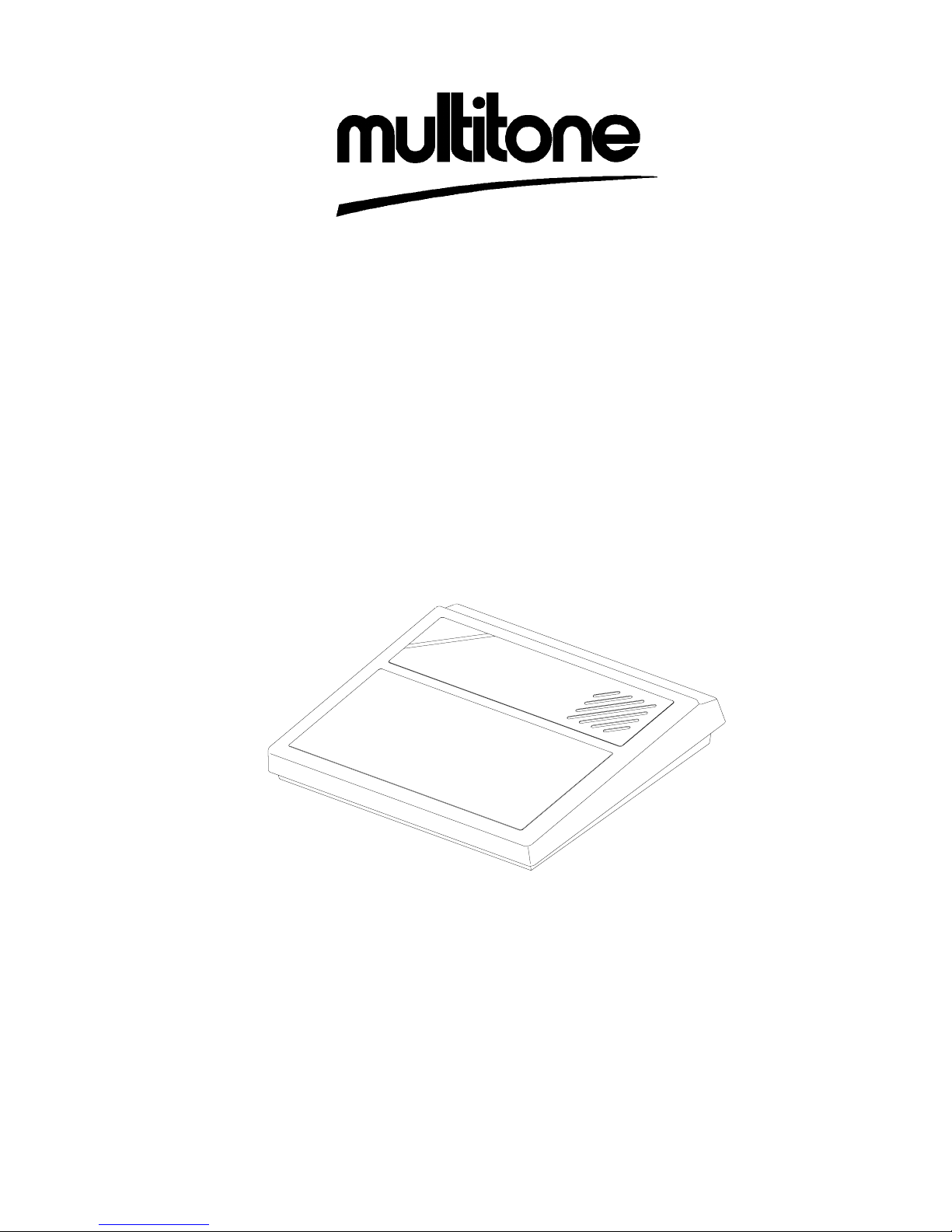
BSR 113
TM1194A Issue B Page (i)
TECHNICAL MANUAL
for
UHF BASE STATION RECEIVER
MODEL BSR 113
(448MHz)
Printed and published in England
Page 2

BSR 113
TM1194A Issue BPage (ii)
COMPANY LIABILITY
The information in this manual has been carefully compiled and checked for technical
accuracy. Multitone Electronics plc accept no l iability for inaccuracies or errors. In line
with the company policy of technical advancement, the information within this document
may be changed. The user should ensure that the correct issue of the document is
used. Comments or correspondence regarding this manual should be addressed to:
Multitone Electronics plc
Technical Publications
Kimbell Road
Basingstoke
Hampshire
RG22 4AD
England
ISSUE DATE
B February 1998
© Multitone Electronics plc 1996, 1998
Page 3

BSR 113
TM1194A Issue B Page (iii)
CONTENTS
Page (I
)
Title Page
Page (ii
)
Company Liabilit
y
Page (iii
)
Contents
Page (iv
)
Effective Page List
Page (v
)
Safety Summar
y
Warnin
g
Page (vi
)
Cautions
Section 1 Introduction and Specification
Section 2 Operating Instructions
Section 3 Technical Description
Section 4 Installation and Commissionin
g
Section 5 Servicin
g
Section 6 Spare Parts List
Section 7 Diagrams
Page 4

BSR 113
TM1194A Issue BPage (iv)
EFFECTIVE PAGE LIST
Page No. Issue Page No. Issue Page No. Issue
(I)
B3-7B5-7B
(ii)
B3-8B5-8B
(
iii
)
B3-9B5-9B
(iv)
B 3-10 B 5-10 B
(v)
B4-1B5-11B
(vi)
B4-2B5-12B
1-1 B 4-3 B 5-13 B
1-2 B 4-4 B 5-14 B
1-3 B 4-5 B 6-1 B
1-4 B 4-6 B 6-2 B
1-5 B 4-7 B 6-3 B
1-6 B 4-8 B 6-4 B
2-1 B 4-9 B 6-5 B
2-2 B 4-10 B 6-6 B
3-1 B 5-1 B 7-1 B
3-2 B 5-2 B 7-2 B
3-3 B 5-3 B 7-3/4 B
3-4 B 5-4 B 7-5/6 B
3-5 B 5-5 B 7-7/8 B
3-6 B 5-6 B 7-9/10 B
7-11 B
Page 5

BSR 113
TM1194A Issue B Page (v)
MANY RESINS AND OTHER CHEMICALS USED IN THE MANUFACTURE OF
ELECTRICAL COMPONENTS FITTED TO THIS BOARD GIVE OFF TOXIC FUMES
WHEN INCINERATED. APPROPRIATE PRECAUTIONS SHOULD T HEREFORE BE
TAKEN WHEN DISPOSING OF THESE ITEMS.
SAFETY SUMMARY
The following information applies to both operating and servicing personnel. General
Warnings and Cautions will be found throughout the manual where they apply.
WARNING statements identify conditions or practices that could result in personal injur
y
or loss of life.
CAUTION statements identify conditions or practices that could result in equipment
damage.
WARNING
Page 6

BSR 113
TM1194A Issue BPage (vi)
CAUTIONS
DO NOT INSTALL THE RECEIVER WHERE IT MAY BE EXPOSED TO LIQUIDS,
STRONG MAGNETIC FIELDS, EXTREME TEMPERATURES OR STRONG SUNLIGHT.
STATIC SENSITIVE DEVICES ARE USED W ITHIN THIS EQUIPMENT. CARE MUST
BE TAKEN TO ENSURE DAMAGE TO THESE DEVICES IS NOT CAUSED BY HIGH
LEVELS OF STAT IC ELECTRICITY. SPARE BOARDS OR CO MPONENTS SHOUL D BE
STORED IN ANTI- STATIC PACKAGING W HEN NOT I NSTAL LED I N THE EQUI PMENT.
DIRECT CONNECTION OF THE BSR 113 TO PUBLIC TELEPHONE OPE RATOR (PTO
)
LINES IS PROHIBITED UNLESS NAT IONAL LINE CONNECTION APPROVAL HAS BEEN
GRANTED BY THE APPROPRIATE REGULATORY AUTHORITY.
UNDER NO CIRCUMSTANCES SHOULD SK1 BE CONNECTED TO THE SYSTEM BUS
OF MULTITONE ACCESS 1000 OR ACCESS 3000 SYSTEMS.
Page 7

BSR 113
TM1194A Issue B Page 1 - 1
SECTION 1
INTRODUCTION AND SPECIFICATION
CONTENTS:
1. INTRODUCTION
2. FEATURES
3. PHYSICAL CONSTRUCTION
SPECIFICATIONS
4. Performance Characteristics
5. Power Supply
6. Connectors
7. Physical Characteristics
8. Operational Environment
FIGURE Page
1. Simplified BSR Configuration 1-2
_______________________
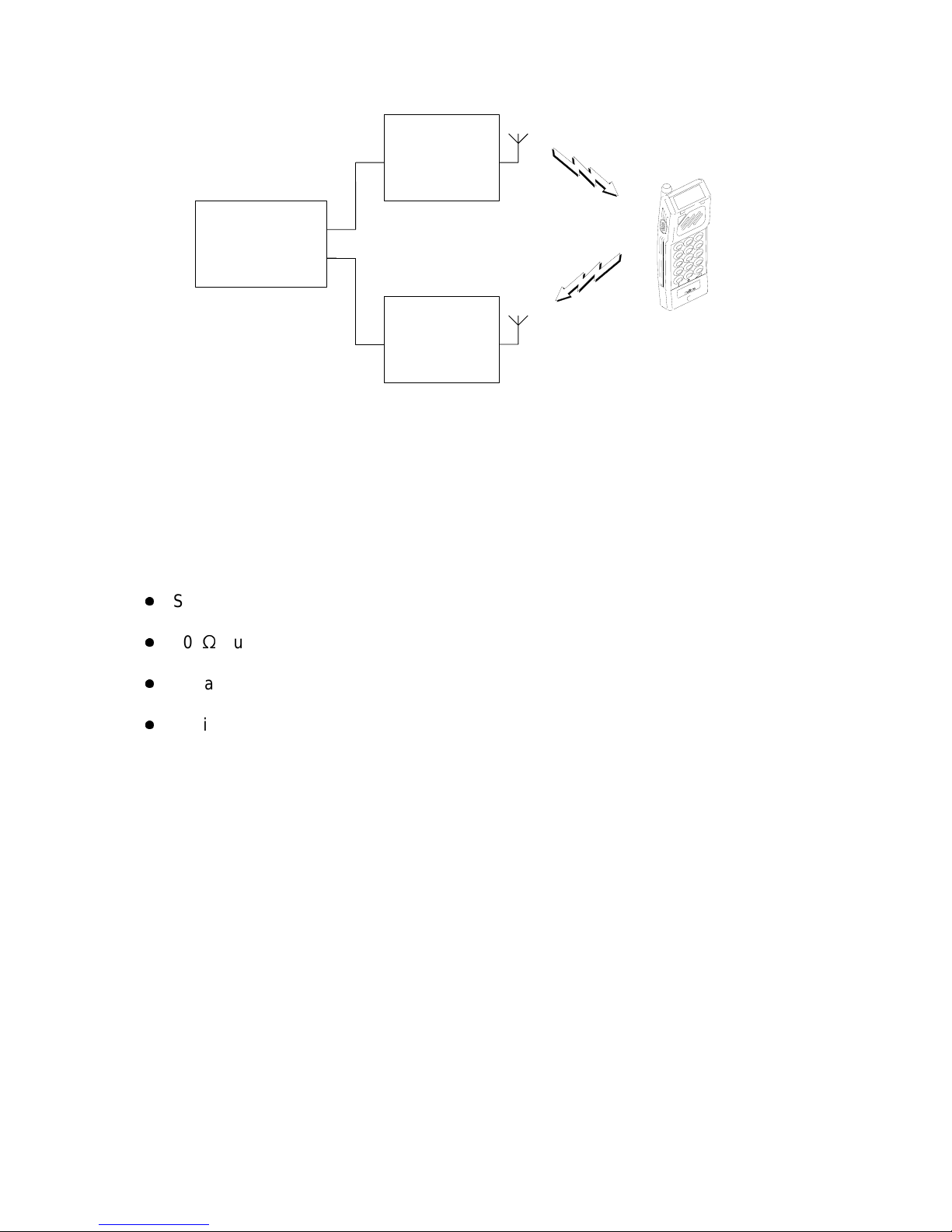
INTRODUCTION
1. The Base Station Receiver model BSR 113 is an UHF double superheterodyne
frequency modulated receiver, operating on a specified frequency within the range
448MHz to 449MHz. The BSR 113 is suitable for systems providing two-way
speech between a base control unit and mobile transceivers, and for systems
incorporating talkthrough between the mobile transcei vers via the base control unit.
A simplified block diagram of a typical BSR 113 configuration is shown in Figure 1.
Page 8
TRANSCEIVER
RECEIVER
STATION
BASE
TRANSMITTER
CONTROL
SYSTEM
TAG10500-2
(e.g. ACCESS 3000)
BSR 113
TM1194A Issue BPage 1 - 2
Figure 1: Simplified BSR Configuration
FEATURES
2. The BSR 113 has the following features:
Signal detect relay
6006 audio line and tone drivers
Speaker with volume control
Ability to link with other receivers
PHYSICAL CONSTRUCTION
3. The BSR 113 consists of a single Pri nted Cir cuit Board (PCB) mounted in a tough,
moulded plastic outer casing, consisting of a base and a cover. The PCB is
mounted on the base and a loudspeaker is fitted to the cover. Connector sockets
are fitted to a cover plate at the rear of the unit. The speaker volume control is
also located at the rear of the unit. The BSR 113 can be wall or shelf mounted.
Page 9

BSR 113
TM1194A Issue B Page 1 - 3
SPECIFICATIONS
Performance Characteristics
4. The performance characteristics of the BSR 113 are as follows:
a) Frequency Range: 448.0 - 449.0MHz
b) Suggested Frequencies: 1: 448.1250MHz
2: 448.1500MHz
3: 448.2250MHz
4: 448.3500MHz
5: 448.6750MHz
c) Channel Spacing: 25kHz
d) Intermediate Frequencies: 1st: 45MHz
2nd: 455kHz
e) Crystal Frequency (1st LO): ƒx = ƒc - 45MHz
6
f) Sub-Audio Tone Frequencies: 88.5Hz, 103.5Hz, 114.8Hz, 127.3Hz,
141.3Hz
g) Sub-Audio Tone Squelch: To EIA standard RS-220
h) Full System Deviation: ±5kHz for 20/25kHz channel spacing
j) Sensitivity (conducted): <1µV for 12dB SINAD at 60% of full
system deviation
k) Tone Squelch Sensitivity: <0.7µV at 15% of full system deviation
l) Adjacent Channel Rejection: >70dB Standard (2 signal method)
m) Spurious Response Rejection: >70dB (2 signal method)
n) Intermodulation Response
Rejection: >60dB (3 signal method)
p) Audio Output (Internal
Loudspeaker): 100mW into 8
6
Page 10

BSR 113
TM1194A Issue BPage 1 - 4
q) Audio Output External Line Level: -13dBm nominal (-4dBm max) to 600
6
(internal, pre-set)
r) Radiated Power to Antenna: <2nW
s) Cabinet Radiation: <2nW
t) Signal Detect Relay Contact Rating: 100V DC, 250mA, non-inductive
Power Supply
5. The power supply requirements of the BSR 113 are as follows:
a) Power Supply: 12V DC
b) Current Consumption: <400mA maximum
Connectors
6. The BSR 113 is fitted with the following connectors:
a) SK2: Audio/Tone Out
b) SK1: Squelch Relay
c) SK3: DC Power Supply
d) SK7: Antenna
Physical Characteristics
7. The physical characteristics of the BSR 113 are as follows:
a) Overall Dimensions: Width: 235mm
Depth: 207mm
Height: 50mm
b) Weight: 0.7kg
Page 11

BSR 113
TM1194A Issue B Page 1 - 5
Operational Environment
8. The environmental characteristics of the BSR 113 are as follows:
a) Operational Temperature Range: -25(C to +55(C
b) Humidity: Up to 95% Relative Humidity over the
operational temperature range
c) Stability: ±6ppm over the operational temperature
range
Page 12

BSR 113
TM1194A Issue BPage 1 - 6
INTENTION ALLY BLANK
Page 13

BSR 113
TM1194A Issue B Page 2 - 1
SECTION 2
OPERATING INSTRUCTIONS
CONTENTS:
1. OPERATION
_______________________
OPERATION
1. The BSR 113 is automatic in operation, with the exception of the following:
a) Switching on the power supply.
b) Setting the volume control (located at the rear of the unit) to a suitable level.
Page 14

BSR 113
TM1194A Issue BPage 2 - 2
INT ENTIO NALL Y BLAN K
Page 15

BSR 113
TM1194A Issue B Page 3 - 1
SECTION 3
TECHNICAL DESCRIPTION
CONTENTS:
1. INTRODUCTION
RADIO CIRCUITRY
2. Signal Input and Isolation
3. RF Amplifier and Filters
4. First Local Oscillator
6. First Mixer
7. Second Local Oscillator and Mixer
8. Second IF Stage
9. Audio Splitting
RX AUDIO PATH
10. Filtering and Amplification
11. Speaker Audio
12. Line Out Driver
NOISE SQUELCH PATH
15. Filtering and Amplification
18. Schmitt Monostable
20. Signal Logic Levels
21. Signal Indication and Noise Squelch Defeat
22. Signal Detect Reed Relay
23. Signal Strength Tone Circuitry
26. Tone Out Driver
SUB-AUDIO TONE PATH
29. Filtering and Amplification
30. Sub-Audio Tone Decoder
32. Sub-Audio Tone Indication and Disable
33. Sub-Audio Tone Squelch Delay Circuit
35. DATA PATH
POWER SUPPLIES
36. +12V Supply
37. +10V Regulator
38. +5V Regulator
39. +1V Internal Reference
Page 16

BSR 113
TM1194A Issue BPage 3 - 2
TABLES Page
1. Noise Squelch Signal Levels 3-8
2. Sub-Audio Tone Frequency Adjustments 3-10
FIGURE
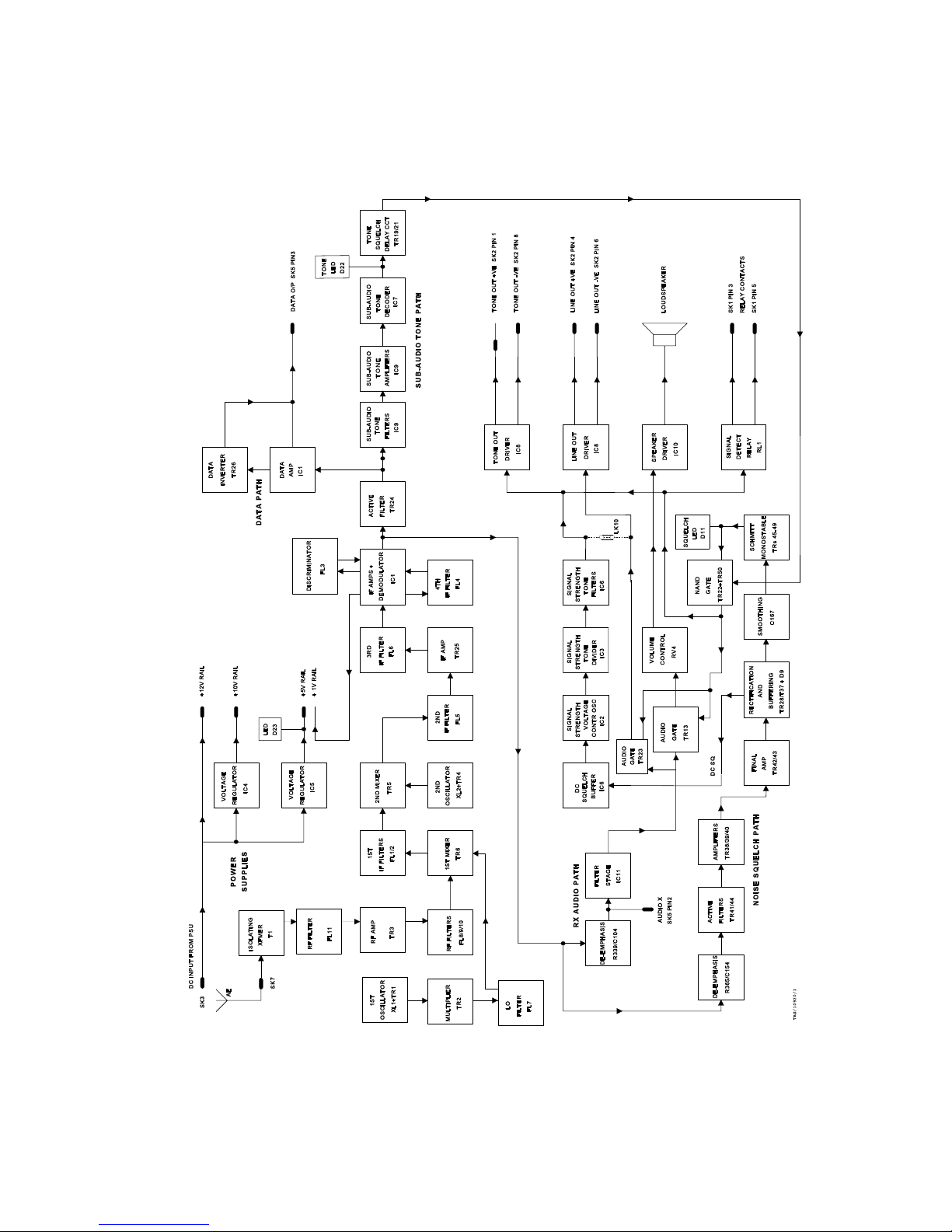
1. Functional Block Diagram 3-2
_______________________
INTRODUCTION
1. This section provides a technical description of the BSR 113 circuit operation.
Reference should be made to the functional block diagram (Figure 1) and the circuit
diagrams in Section 7.
RADIO CIRCUITRY
Signal Input and Isolation
2. The incoming RF signal is detected by an external antenna connected to
socket SK7, from where the signal passes through an isolating transformer (T1)
which improves immunity to Electro-Static Discharge (ESD). The signal is then fed
to the first RF helical fi lter, FL11, which protects the RF amplifier fro m str ong out-ofband signals.
RF Amplifier and Filters
3. Impedance matching is provided by L15, L16 and associated components. The RF
signal is amplified by TR3 and then fil tered by the helical fil ters FL8, FL9 and FL10.
They provide a degree of selectivity before passing the signal to the first mixer.
First Local Oscillator
4. The first local oscillator comprises TR1, XL1 and associated components.
Frequency adjustment is provided by C3. The collector o f TR1 is t uned to the third
harmonic of XL1 by C9 and L6. The output of TR1 is then doubled by TR2 to
provide the correct injection frequency for the first mixer.
5. The frequency of the crystal is calculated by using the following formula:
Crystal (XL1) frequency (MHz) = Receiver Channel Frequency (MHz) - 45MHz
6
Page 17
BSR 113
TM1194A Issue B Page 3 - 3
Figure 1: Functional Block Diagram
Page 18

BSR 113
TM1194A Issue BPage 3 - 4
First Mixer
6. The first mixer comprises TR6 and associated components. The i njecti on fr equency
from the first local oscillator is fed to the first mixer via the helical filter FL7 and
inductor L9. The RF signal is input via the inductor L13. The difference signal of
45MHz is selected by the collector load of L12, R18 and C29. The 45MHz is then
filtered by FL1 and FL2 to remove unwanted signals.
Second Local Oscillator and Mixer
7. The second local oscillator is formed by TR4, XL2 and associated components. It
runs at a fixed frequency of 44.545MHz. The signal is selected from the collector
of TR4 and input, along with the RF from FL2, onto the base of mixer TR5. The
difference signal of 455kHz then passes to FL5, with matching provided by R31.
Second IF Stage
8. The second IF chain comprises three ceramic filters of channel bandwidt h, FL5 , FL6
and FL4, each followed by an IF amplifier. After FL5 the 455kHz IF signal is
amplified by the low noise transistor TR25 and then passed to FL6. The signal is
then fed to IC1 (pin 1) where the r emaining IF amplifi cation and amplitude limiting
are provided. Another stage of filtering is carried out by FL4. Demodulation is
carried out using the ceramic discriminator FL3 as the quadrature network for the
on-chip demodulator. After demodulation the signal is output from IC1 (pin 14).
Audio Splitting
9. The demodulated audio signal leaves IC1 (pin 14) and divides three ways:
a) To a de-emphasis circuit (comprising R339 and C104) and the Rx Audio path.
b) To a de-emphasis circuit (comprising R365 and C154) and the Noise Squelch
path.
c) To an active fi lter (comprising TR24, C82, C83, R341 and R344) where it then
divides two ways:
i) To the Sub-Audio Tone path.
ii) To the Data path.
Page 19

BSR 113
TM1194A Issue B Page 3 - 5
RX AUDIO PATH
Filtering and Amplification
10. The audio si gnal is de-emphasised by R339 and C104 to produce the test and tune
up signal Audio X (available at the i nternal test socket SK5 pin 2) . It also passes
through two stages of high pass filtering and two stages of low pass filtering,
provided by IC11 (pin 8) and IC11 (pin 14), to become the Rx Audio signal. The
fitting of link LK4 enables the signal to bypass the high pass filter stage IC11 (pin
1) (for future applications). IC11 (pin 7) acts as a buffer amplifier.
Speaker Audio
11. The Rx Audio output from IC11 (pin 14) is fed, via the audio gate TR13, to the
input of an operational-amplifier circuit, IC10, via R93 and RV4. Variable resistor
RV4 provides volume control. The speaker driver uses a bridge technique to
provide maximum voltage swing on the speaker driver output. Resistors R168,
R169, R170 and R171 are load protection for IC10 to prevent any damage to the
chip resulting from over dissipation.
Line Out Driver
12. The Rx Audio output from IC11 (pin 14) is also fed, via the audio gate TR23 and
RV6, to the Line Out driver amplifier IC8. In normal operation link LK2 i s fitted and
the Line Out signal is gated by the noise Squelch, via gate TR18. Alt ernati vely, the
signal can be continuously enabled by removing link LK2.
13. The output of IC8 (pin 1) is passed to the l ine termination loading and safe ty bar rier
circuitry provided by components R104, R105, R106, R107, R108, R109, C242,
C243, C244, CS4 and T4. The Line Out signal then proceeds to the external line
connection via SK2 (pins 4 and 6).
14. The links LK22, LK23, LK24, and LK25 are intended for setting the Line Out
termination loading when connecting to Public Telephone Operator (PTO) lines in
different countries (subject to national li ne connection approval). For further details
refer to Section 4. In normal operation Link LK5 is fitted and is removed only for
factory test purposes. The Tone Out signal is combined with the Line Out signal
by the fitting of link LK10 (refer to Section 4).
Page 20

BSR 113
TM1194A Issue BPage 3 - 6
NOISE SQUELCH PATH
Filtering and Amplification
15. The audio si gnal from IC1 (pin 14) is de-emphasised by R365 and C154. It is then
filtered by the active filter stages TR41 and TR44 to pass only frequencies above
approximately 6kHz. These stages give approximately 60dBs of rejection of low
frequency audio relative to the high audio frequencies used by the s quelch circuitry.
Adjustment of the noise Squelch signal is provided by RV2.
16. From the active filtering stages the audio is amplified by the successive stages
TR40, TR39 and TR38 to produce a high level noise signal at the collector of
TR38. All of these stages are designed to have very stable gain and frequency
response over the operational temperature range.
17. After passing through C163 the signal is fed to the final gain stage TR42, TR43,
which has been configured to have a very stable DC operating point so that the
peak-to-peak noise on the output is very stable with temperature change. The
resulting high level signal is then rectified and buffered by D9, TR37 and TR28,
again with special care being taken of temperature performance. The rectified
signal is smoothed by C167.
Schmitt Monostable
18. The following stage (comprising TR45, TR46, TR47, TR48, TR49 and TR50) is
configured as a Schmitt monostable. When the DC level goes above the level
determined by R373 and R414, then TR36 and TR47 are turned on thus holding
TR45 on and providing hysteresis. As the DC level decreases again R417 stops
TR45 turning off until a lower level is reached than that required to turn it on.
When TR36 collector goes low (i.e. during high noise/low Rx signal strength
conditions), TR48 turns on charging C106 and turning off TR49. This then turns
off TR50 and produces the noise Squelch signal on the collector of TR50.
19. The high levels of amplification are required to enable the noise Squelch to work
on strong RF signals where there is a great deal of quieting. This ensures that
sub-standard audio signals are not output to the system.
Signal Logic Levels
20. The time constants provided by C106 and R420 ensure that the audio is not
enabled until the carrier has been detected for more than approximately 50ms. T his
ensures the minimum of squelch bounce in noisy conditions. The logic level s at t he
collector of TR50 for the noise Squelch signal are as shown in Table 1.
Page 21

BSR 113
TM1194A Issue B Page 3 - 7
Table 1: Noise Squelch Signal Levels
LEVEL SIGNAL
5V NOT RECEIVED
0V RECEIVED
Signal Indication and Noise Squelch Defeat
21. When the collector of TR49 goes high TR27 is turned on allowing current to flow
through the LED D11, thus providing a receive signal indication. The collector of
TR49 can also be held permanently high by fitting LK1, providing a noise Squelch
defeat facility.
Signal Detect Reed Relay
22. W hen a squelch signal of 0V (i.e. signal received by the receiver) is pl aced on the
base of TR11 it is switched off. This in turn places +5V on the base of TR12
which switches on, allowing current to flow through the relay coil of RL1. When
current flows the relay contacts close. The contacts are connected to auxiliary
socket SK1 (pins 3 and 5).
Signal Strength T one Circuitry
23. The rectified output from the collector of TR28 is known as DC SQ and is fed to
a DC buffer (IC6). The resulting DC level is passed to IC2 (pin 5) which acts as
a Voltage Controlled Oscillator (VCO) running at approximately 12kHz. The
frequency of the output (pin 3) is dependent on the DC level of the input (pin 5).
A higher level of incoming DC squelch signal produces a lower frequency oscillator
output, and vice-versa.
24. IC3 is a quad D-type flip-flop which divides the VCO output by four to obtain
approximately 3kHz and provides a square wave output. The signal then passes
through two stages of band-pass filtering provided by IC6.
25. The frequency of the signal strength tone output varies from about 2.7kHz for a
receiver RF input level of approximately -100dBm (and above) to approximately
3.2kHz for an input level of approximately -120dBm (and below). Fine adjustment
of the signal strength tone frequency is provided by RV1.
Tone Out Driver
26. The output from the Signal Strength Tone circuitry is fed, via audio gate TR30, to
the Tone Out driver amplifier IC8 (pin 5). In normal operation link LK14 is fitted
and the Tone Out signal is gated by the noise Squelch vi a gat e TR18 or th e si gnal
is continuously running dependent upon the application. For ful l vot ing LK 14 is out.
Page 22

BSR 113
TM1194A Issue BPage 3 - 8
27. The output of IC8 (pin 7) is passed to the l ine termination loading and safe ty bar rier
circuitry provided by components R98, R99, R100, R101, R102, R103, C239, C240,
C241, CS3 and T3. The Tone Out signal then proceeds to the external line
connection via SK2 (pins 1 and 8). Transistors TR16, TR17 and associated
components provide soft limiting to the signal if TR16 is optionally fitted.
28. Links LK6, LK7, LK19, and LK20 are intended to set the Tone Out termination
loading when connecting to PTO lines in diffe rent c ountries (subject to national line
connection approval). For further details refer to Section 4. In normal operation
Link LK5 is fitted and is removed only for factory test purposes. If required, the
Tone Out signal can be combined with the Line Out signal by the fitting of link
LK10 (refer to Section 4).
SUB-AUDIO TONE PATH
Filtering and Amplification
29. From the active filter TR24 the Sub-Audio signal is fed through two stages of lowpass filtering provided by IC9 (pin 1) and IC9 (pin 7). The signal then passes
through two stages of amplification provided by IC9 (pin 14) and IC9 (pin 8) and
is then fed to a potential divider R158, R159. This divider reduces the amplitude
of the signal to the correct level required for input to the decoder circuitry.
Sub-Audio Tone Decoder
30. The signal is fed into IC7 (pin 3) via C284, R158, R159 and C289. The ratio of
R158 to R159 determines the tone signal level at the input of IC7. T his d etermin es
the RF signal input level to the receiver at which the tone opens. The frequency
of the tone which can be detected is determined by the CR network R163, R164,
R165, RV5 and C285. Table 2 specifies which resistors must be shorted out by
links LK8 and LK9 in order to detect the correct tone frequency. Fine adjustment
is provided by RV5.
Table 2: Sub-Audio Tone Frequency Adjustments
SUB-AUDIO TONE FREQUENCY LINKS FITTED
88.5Hz NONE
103.5Hz LK8
114.8Hz LK8
127.3Hz LK8
141.3Hz LK8 AND LK9
Page 23

BSR 113
TM1194A Issue B Page 3 - 9
31. The tone frequency is calculated as follows:
Tone Frequency (Hz) = 1
2.8 x C285 x (R163 + RV5 + Rt)
where Rt = R165 or, R164 and R165 (refer to Table 2).
Sub-Audio Tone Indication and Disable
32. Capacitors C286 and C287 determine the cut-off points of fi lter s inte rnal to the tone
decoder IC7. The output of IC7 (pin 8) is a switch (TR19) to ground which is
activated when an input tone of the correct frequency is detected. The output of
IC7 has a load resistor R161 which is connected to +5V. This allows the output
voltage to be +5V when there is no tone present at the input and 0V when a tone
is present, thus allowing current to flow through the LED D22 and providing a Tone
Detect indication. IC7 (pin 8) can be shorted to ground by fitting LK3 providing a
Tone Disable facility.
Sub-Audio Tone Squelch Delay Circuit
33. W hen there is no Sub-Audio Tone detected by IC7 its output (pin 8 ) is h igh, puttin g
a high on the base of TR19 and charging capacitor C288. When a Sub-Audio
Tone is detected by IC7 its output is pulled low, switching TR19 off and causing
C288 to discharge slowly through R140. This signal rect ifica tion means that a high
on the base of TR19 produces a long pulse through TR21 and the NAND gate
TR22, which switches off the squelch signal via the emitter of TR50.
34. As a protection against the false detection of Sub-Audio Tones, the circuit places
a 150ms delay between the output of IC7 going low and the squelch going low.
If IC7 pulls the output low with a false detection and this detection lasts less than
150ms then C288 does not have enough time to discharge before TR19 switches
on and the capacitor charges again, preventing the squelch line going low. The
emitter of TR50 is connected to the collector of TR22 ensuring that TR50 is
switched on only if both the noise Squelch and tone Squelch are open.
DATA PATH
35. The output of the active filter (TR24 and associated components) is fed via C96 to
the on-chip data amplifier of IC1. Selection of either R350 or R351 determines
whether the data amplifier output is inverted. If R350 is fitted the output of the
amplifier is passed directly to the internal test socket SK5 pin 3. If R351 is fitted
the output of the amplifier is passed to the data inverter TR26, before being fed to
SK5. The data signal is intended for future applications only.
Page 24

BSR 113
TM1194A Issue BPage 3 - 10
POWER SUPPLIES
+12 Supply
36. The +12V regulated input voltage from the Powe r Supply Unit (PSU) is fed into the
BSR via SK3 and FS1. It is then passed to the voltage regulators.
+10V Regulator
37. Voltage regulator IC4 converts its +12V regulated input to +10V, which is then
passed to the rest of the circuitry.
+5V Regulator
38. Voltage regulator IC5 converts its +12V regulated input to +5V, which is then
passed to the rest of the circuitry. Indication of the +5V rail is provided by LED
D23.
+1V Internal Reference
39. The +1V line used by most of the receiver is generated by an internal reference
and driver circuit in IC1. Transistor TR20 acts as the output stage controlled by
IC1 (pin 19). The sense input is via R366 to IC1 (pin 18).
Page 25

BSR 113
TM1194A Issue B Page 4 - 1
SECTION 4
INSTALLATION AND COMMISSIONING
CONTENTS:
1. GENERAL
2. INSTALLATION
3. Shelf Mounting
4. W all Mounting
5. Power Supply Connection
7. Antenna Connection
8. Audio Connection
9. External Line Connection
12. Auxiliary Connection
13. Sub-Audio Tone Frequency Adjustments
14. COMMISSIONING
TABLES Page
1. Summary of Link Settings 4-6
2. Line Out/Tone Out Termination Loading - Link Settings 4-8
3. Pin Descriptions 4-9
FIGURES
1. Wall Mounting Hole Positions 4-3
2. Single BSR 113 Configuration 4-4
3. Multiple BSR 113 Configuration 4-5
4. Link Positions 4-7
5. Socket Positions 4-9
6. 8-Way Modular Plug (FCC68 Type) Pin Configuration 4-10
_______________________
GENERAL
1. This secti on details the installation and commissioning procedures for the BSR 113.
Refer to Figure 5 for the BSR 113 socket positions and Table 3 for the pin
descriptions of each socket.
Page 26

BSR 113
TM1194A Issue BPage 4 - 2
INSTALLATION
2. The BSR 113 can be either shelf or wall mounted. Ensure that i t is mounted within
three metres of an AC mains power supply outlet.
CAUTION
DO NOT INSTALL THE RECEIVER WHERE IT MAY BE EXPOSED TO LIQUIDS,
STRONG MAGNETIC FIELDS, EXTREME TEMPERATURES OR STRONG
SUNLIGHT.
CAUTION
STATIC SENSITIVE DEVICES ARE USED WITHIN THIS EQUIPMENT. CARE
MUST BE TAKEN TO ENSU RE DAM AGE T O THESE DEVICES IS NOT CAUSED
BY HIGH LEVELS OF STATIC ELECTRICITY. SPARE BOARDS OR
COMPONENTS SHOULD BE STORED IN ANTI -STAT IC PA CKAGI NG W HEN N OT
INSTALLED IN THE EQUIPMENT.
Shelf Mounting
3. The base of the BSR 113 is fitted wi th four r ubber feet that provide a non-slip grip
on a flat surface suitable for shelf mounting.
Wall Mounting
4. To wall mount the BSR 113 proceed as follows:
a) Referring to Figure 1, mark, drill and plug the four fixing holes.
b) Remove the four rubber feet from their retaining holes on the base of the
receiver.
c) Remove the two screws located at the rear of the receiver and carefully lift the
cover off, taking care not to detach the speaker wires.
d) Screw the base of the receiver directly onto the wall using 4mm round/pan
head screws, taking care n ot to damage the PCB. Four clearance holes have
been pre-cut into the PCB to allow the screws access through to the receiver
base.
e) Replace the receiver cover by fitting the front of the cover onto the base first
and then bringing the rear of the cover down onto the rear of the base,
ensuring that back cover plate is correctly seated. Replace the two screws at
the rear of the receiver.
Page 27

136mm
164mm
TAG/10821/1
BSR 113
TM1194A Issue B Page 4 - 3
Figure 1: Wall Mounting Hole Positions
Power Supply Connection
5. The BSR 113 must be fitted with the 12V DC 640mA Power Supply Unit (PSU),
Part No. 6601-0011 (UK) or Part No. 6603-0003 (Europe). No other PSUs are
acceptable for use.
6. To connect the PSU insert the PSU plug into socket SK3, sited approximately 35mm
in from the rear panel. Check that the plug is captive and s ecure the po wer supply
cable in place using a small nylon tie wrap (Part No. 36904) so that it does not
inadvertently disconnect.
Antenna Connection
7. Connect the antenna to the 506 BNC connector, SK7, situated at the rear of the
BSR 113. Alternatively, fit the BNC N-typ e coaxi al ca ble f or an extended antenna.
No external braid breaker is required as it is built in the unit.
Audio Connection
8. The audio output (SK2) of the unit can be connected in one of t wo ways depending
upon the receiver requirements of the system i.e. a single or multiple receiver
configuration. SK2 is an 8-way modular socket (FCC68 type). Refer to Figure 6
for details of the equivalent plug pin configuration. Any new system using more
than one BSR 113, together with RPR 560 transceivers, must use a P317 Voting
Unit to connect the BSRs to the system. The BSR 113 is backwards compatible
with existing systems and may use existing methods of combining the BSRs
provided RPR 560s are not added to the system.
Page 28

ACCESS 1000
or
ACCESS 3000
MODULAR
JUNCTION
BOX
TAG10921-2
BSR 113
SK2
SYSTEM BUS
AUDIO
PSU
AE
SK7
SK3
BSR 113
TM1194A Issue BPage 4 - 4
Figure 2: Single BSR 113 Configuration
a) Single Receiver Configuration
If the system requires only one BSR 113, connect SK2 directly to the system
bus (Access 1000 or Access 3000) via a modular junction box
(Part No. 4509-0003) using an 8-way modular plug (FCC68 type) double ended
cable (Part No. 0301-0580), as shown in Figure 2. Refer to the appropriate
Technical Manual for the system bus details.
b) Multiple Receiver Configuration
A multiple receiver configuration uses the Voting method of receiver selection.
A maximum of eight BSRs can be connected to a P317 Voting Unit and up to
two P317s can be connected to a system, giving a maximum of 16 BSRs.
Remove LK14 to select Voting operation. Refer to Table 1.
If the system requires more than one BSR 113, connect SK2 of each BSR 113
to a P317 Voting Unit using an 8-way modular plug (FCC68 type) double ended
cable (Part No. 0301-0580). Connect the P317 to the system bus
(Access 1000 or Access 3000) as shown in Figure 3. Refer to the appropriate
Technical Manual for the system bus details and the P317 Voting Unit.
Page 29

SK2
BSR 113
PSU
AE
SK7
SK3
SK2
BSR 113
PSU
AE
SK7
SK3
SK2
BSR 113
PSU
AE
SK7
SK3
SK2
BSR 113
PSU
AE
SK7
SK3
SK2
BSR 113
PSU
AE
SK7
SK3
P317
VOTING UNIT
P317
VOTING UNIT
PSU
PSU
CONTROL
UNIT
CONTROL
UNIT
AUDIO+
TONE
AUDIO
SYSTEM
BUS
ACCESS 1000
OR
ACCESS 3000
RECEIVERS
5 TO 8
BSR 113
TM1194A Issue B Page 4 - 5
Figure 3: Multiple BSR 113 Configuration
Page 30

BSR 113
TM1194A Issue BPage 4 - 6
Table 1: Summary of Link Settings
LINK POSITION EFFECT
1
IN * NOISE SQUELCH DEFEATED
OUT NOISE SQUELCH ACTIVE
2
IN * LINE OUT G ATED BY SQUELCH
OUT LINE OUT CONTINUOUSLY ENABLED
3
IN SUB- AUDIO TONE DISABLED
OUT * SUB-AUDIO TONE ENABLED
4
IN
RX AUDIO HIGH PASS FILT ER STAGE BYPASSED
(FOR FU TURE APPLICATIONS)
OUT * RX AUD IO HIGH PASS FILTER STAGE OPERATIVE
5
IN * NORMAL OPERAT ION
OUT FACTOR Y TEST PU RPOSES ONLY
6, 7, 19 & 20 REFER TO TABLE 2
TONE OUT TERMINATION LOADING FOR
NATIONAL PT O LINES
8 & 9 SUB-AUDIO TONE SELECTION
REFER TO SECTION 3,
TABLE 2
10
IN * LINE OUT AND TONE OUT COMBINED
OUT LINE OUT AND T ONE OUT SEPARAT ED
14
IN SIGNAL STREN GTH TONE G ATED BY SQUELCH
OUT *
SIGNAL STRENGTH TONE NOT GATED BY
SQUELCH
22, 23, 24 & 25 REFER TO TABLE 2
LINE OUT TERMINATION LOADING FOR
NATIONAL PT O LINES
* = Default Position.
Page 31

TAG/10923/1
BSR 113
TM1194A Issue B Page 4 - 7
Figure 4: Link Positions
External Line Connection
9. The audio output of the BSR 113 can also be connected directly to lines external
to the system, such as privat e wire lin es pro vided by a Public Telephone Operator
(PTO). This allows the audio signals to be passed from a remote BSR 113 to the
local system via the external lines. The system must be connected to the PTO
lines via a P317 Voting Unit.
CAUTION
DIRECT CONNECTION OF THE BSR 113 TO PUBLIC TELEPHONE OPERATOR
(PTO) LINES IS PROHIBITED UNLESS NATIONAL LINE CONNECTION
APPROVAL HAS BEEN GRANTED BY THE APPROPRIATE REGULATORY
AUTHORITY.
Page 32

BSR 113
TM1194A Issue BPage 4 - 8
10. The Line Out and Tone Out si gnals each require a PTO line to be connecte d to th e
appropriate pins of socket SK2. Alternatively, the Tone Out signal can be c ombined
with the Line Out signal by the fitting of link LK10. This allows both signals to be
fed from the Line Out pins (4 and 6) to one PTO line instead of two.
11. The Line Out and Tone Out termination loading link settings are pre-set during
manufacture to meet the requirements set by the regulatory authority of the
appropriate country, and should not require resetting during installation. However,
the range of possible link settings are detailed in Table 2.
Table 2: Line Out/Tone Out Termination Loading - Link Settings
COUNTRY LK22/LK6 LK23/LK7 LK24/LK19 LK25/LK20
UNITED KINGDOM 1-2 OUT OUT IN
GERMANY 1-2 IN OUT OUT
AUSTRIA 1-2 IN OUT OUT
BELGIUM 1-2 IN OUT OUT
SPAIN 1-2 IN OUT OUT
ITALY 2-3 N/A OUT N/A
NETHERLANDS 2-3 N/A OUT N/A
Auxiliary Connection
CAUTION
UNDER NO CIRCUMSTANCES SHOULD SK1 BE CONNECTE D TO THE SYSTEM
BUS OF THE ACCESS 1000 OR ACCESS 3000 SYSTEMS.
12. Auxiliary socket SK1 contains the connections to the Signal Detect Reed Relay
contacts. SK1 is an 8-way modular socket (FCC68 type), refer to Figure 6 for
details of the equivalent plug pin configuration.
Sub-Audio Tone Frequency Adjustments
13. The sub-audio tone frequency adjustments are pre-set during manufacture and
should not require resetting during installation. If required, details of the
adjustments are given in Section 3. The sub-audio tone can be disabled by fitting
link LK3.
Page 33

VOLUME CONTROL
1
SK2
SK3
SK1
RV4
1
AERIAL
TAG/10491/1
SQUELCH RELAY
DC INPUTAUDIO OU T
REAR VIEW
BSR 113
TM1194A Issue B Page 4 - 9
Figure 5: Socket Positions
COMMISSIO NING
14. The BSR 113 requires no commissioning other than switching on the PSU and
setting the volume control (RV4), located at the rear of the unit, to the required
level.
Table 3: Pin Descriptions
PIN
NUMBER
SK2 SK3 SK1 SK7
AUDIO/TONE DC AUXILIARY ANTENNA
OUT POWER
1
Tone +12V Not
Out + connected
506 RF I/P
2
Not Not
connected connected
3
Not 0V Relay
connected Contact
4
Line Not
Out + connected
5
Not Relay
connected Contact
6
Line Not
Out - connected
7
Not Not
connected connected
8
Tone Not
Out - connected
Page 34

8 7 6 5 4 3 2 1
PIN
VIEWED FROM
NON-CLIP SIDE
CLIP ON
OTHER SIDE
TAG/10493/1
BSR 113
TM1194A Issue BPage 4 - 10
Figure 6: 8-Way Modular Plug (FCC68 Type) Pin Configuration
Page 35

BSR 113
TM1194A Issue B
Page 5 - 1
SECTION 5
SERVICING
CONTENTS:
1. ROUTINE MAINTENANCE
2. SERVICE POLICY
3. W ORKSHOP PROVISIONS
TEST EQUIPMENT, TOOLS AND ANCILLARIES
4. Test Equipment
5. Tools and Ancillaries
SERVICING
6. Removal and Replacement of Receiver Cover
7. PCB Removal and Replacement
8. ALIGNMENT PROCEDURES
9. Receiver and Noise Squelch Alignment
10. Sub-Audio Tone Alignment
11. Signal Strength Tone Alignment
12. Line Out Level Alignment
13. FAULT-FINDING
15. EXTERNAL LINE TESTING
TABLE Page
1. Test Signals 5-4
FIGURES
1. Receiver and Noise Squelch Alignment Test Equipment 5-5
2. Sub-Audio Tone Alignment Test Equipment 5-7
3. Signal Strength Tone/Line Out Level Alignment Test Equipment 5-8
4. ICs 1 to 3 - Pin Configurations 5-11
5. ICs 4 to 11 - Pin Configurations 5-12
6. Transistor Pin Configuration 5-13
Page 36

BSR 113
TM1194A Issue B
Page 5 - 2
MANY RESINS AND OTHER CHEMICALS USED IN THE MANUFACTURE OF
ELECTRICAL COMPONENTS FITTED TO THIS BOARD GIVE OFF TOXIC
FUMES WHEN INCINERATED. APPROPRIATE PRECAUTIONS SHOULD
THEREFORE BE TAKEN WHEN DISPOSING OF THESE ITEMS.
CAUTION
STATIC SENSITIVE DEVICES ARE USED WITHIN THIS EQUIPMENT. CARE
MUST BE TAKEN TO ENSURE DAMAGE TO THESE DEVICES IS NOT CAUSED
BY HIGH LEVELS OF STATIC ELECTRICITY. SPARE BOARDS OR
COMPONENTS SHOULD BE STORED IN ANTI-STATIC PACKAGING W HEN NOT
INSTALLED IN THE EQUIPMENT.
WARNING
ROUTINE MAINTENANCE
1. Routine maintenance is limited to surface cleaning of the receiver using a lint-free
cloth moistened with soap-free water.
SERVICE POLICY
2. The service policy for the BSR 113 is to repair the equipment to component level.
Repairs are only to be performed by qualified personnel in authorised workshops.
WORKSHOP PROVISIONS
3. Repair workshops must be free from hostile radio interference or otherwise equipped
with Faraday cages. Suitab le equipment must be available to remove and replace
the surface mount components which are used in this receiver.
Page 37

BSR 113
TM1194A Issue B
Page 5 - 3
TEST EQUIPMENT, TOOLS AND ANCILLARIES
Test Equipment
4. The following test equipment is required to carry out the servicing procedures:
&
Radio Frequency (RF) Signal Generator (frequency range up to 200MHz)
&
Frequency Counter (capable of measuring between 100Hz and 350Hz)
&
SINAD Meter (with loudspeaker)
&
Oscilloscope
&
12V DC Power Supply (Multitone Part No. 6601-0011 or 6603-0003)
&
Multimeter
Tools and Ancillaries
5. The following tools and ancillaries are required to carry out the servicing
procedures:
&
Surface Mount Handling Tools
&
Anti-static Workstation
&
Modular Test Plug/Cable
NOTE: Use an 8-way modular plug (FCC68 type) single ended cable (Part No.
0301-0092) as the Modular Test Plug/Cable.
SERVICING
Removal and Replacement of Receiver Cover
6. To remove and replace the receiver cover proceed as follows:
a) Remove the two screws located at the rear of the receiver and care fully remove
the cover, taking care not to detach the speaker wires (if fitted).
b) To replace the cover locate the front onto the case chassis first. Swing the
cover down onto the back of the chassis, ensuring that the back cover plate is
correctly located. Replace the two screws at the rear of the receiver.
Page 38

BSR 113
TM1194A Issue B
Page 5 - 4
PCB Removal and Replacement
7. To remove the Printed Circuit Board (PCB) proceed as follows:
a) Remove the receiver cover (refer to `Removal and Replacement of Receiver
Cover').
b) Remove the three screws which hold the PCB to the bottom of the case and
carefully slide out the PCB.
c) Replacement is the reverse of the removal procedure.
ALIGNMENT PROCEDURES
8. Perform the alignment procedures for the BSR 113 in the same order as shown.
Check the +10V and +5V power supplies before proceeding. The +5V power
supply is also indicated by the illumination of LED D23. Refer to Table 1 for the
test signals.
NOTE: Insert the Modular Test Plug/Cable into the internal test socket SK5. T he
open end of the cable can be used for connecting test equipment to the
pins of SK5.
Table 1: Test Signals
TEST DESC RIPTION TEST SOC KET
POINT SK5 PIN
TP1 +5V DC 4
TP2 +10V DC 5
TP3 SUB-AUDIO TONE FREQUENCY x 2 = 8
SQUARE W AVE of 4V p-p
TP4 GROUND 1
TP5 SPEAKER AUDIO 1 N/A
TP6 SPEAKER AUDIO 2 N/A
N/A DATA 3
N/A AUDIO X 2
N/A N OISE SQUELCH SIGNAL 6
Page 39

SIGNAL
RF O/P
PSU
12V
BSR 113
SINA D METER
and
OSCILLOSCOPE
BNC
CABLE
SK7
MOD I/P
1kHz from SINA D M ETER
SK3
GENERATOR
TAG/10924/1
SK5-2
SK5-1
BSR 113
TM1194A Issue B
Page 5 - 5
Figure 1: Receiver and Noise Squelch Alignment Test Equipment
Receiver and Noise Squelch Alignment
9. To carry out the receiver alignment procedure configure the equipment as shown
in Figure 1 and proceed as follows:
a) Connect the oscilloscope (using a DC coupled x1 probe) and the SINAD meter,
across internal test socket SK5 Pins 2 (Audio X) and 1 (GND).
b) Set the signal generator to a signal of +13dBm at the on-channel frequency
modulated with 1kHz at a deviation of 3kHz.
NOTE: If the SINAD meter is used for generating the external 1kHz, set the
correct level into the signal generator by turning the MOD ALC
(modulation automatic level control) on and then adjusting the level
from the SINAD meter until 3kHz FM is indicated rather than Hi or
Lo.
c) Connect the signal generator to the antenna socket SK7.
d) Adjust C3 until the recovered audio on the oscilloscope is at a DC level of
0.62V.
e) Decrease the RF level from the signal generator to achieve 12dB SINAD.
f) Adjust C9 for best SINAD and then reduce the RF level from the signal
generator to maintain about 12dB SINAD.
Page 40

BSR 113
TM1194A Issue B
Page 5 - 6
g)
FL7
:
I) Adjust the first slug of FL7 for best SINAD. Ensure that the best tuning
point is found by first adjusting the slug from one extr eme of t ravel to th e
other.
ii) Reduce the RF level from the signal generator to maintain about 12dB
SINAD.
iii) Repeat (I) and (ii) for the second slug of FL7.
h)
FL11
:
I) Adjust the first slug of FL11 for best SINAD. Ensur e that th e best tuni ng
point is found by first adjusting the slug from one extr eme of t ravel to th e
other.
ii) Reduce the RF level from the signal generator to maintain about 12dB
SINAD.
iii) Repeat (I) and (ii) for the second slug of FL11.
j)
FL8
:
I) Adjust the first slug of FL8 for best SINAD. Ensure that the best tuning
point is found by first adjusting the slug from one extr eme of t ravel to th e
other.
ii) Reduce the RF level from the signal generator to maintain about 12dB
SINAD.
iii) Repeat (I) and (ii) for the second slug of FL8.
k)
FL9
:
I) Adjust the first slug of FL9 for best SINAD. Ensure that the best tuning
point is found by first adjusting the slug from one extr eme of t ravel to th e
other.
ii) Reduce the RF level from the signal generator to maintain about 12dB
SINAD.
iii) Repeat (I) and (ii) for the second slug of FL9.
Page 41

BSR 113
TM1194A Issue B
Page 5 - 7
l)
FL10
:
I) Adjust the first slug of FL10 for best SINAD. Ensur e that th e best tuni ng
point is found by first adjusting the slug from one extr eme of t ravel to th e
other.
ii) Reduce the RF level from the signal generator to maintain about 12dB
SINAD.
iii) Repeat (I) and (ii) for the second slug of FL10.
m) Set the RF level from the signal generator to -50dBm.
n) Repeat (d) to (l).
p) Set the RF level from the signal generator to 5dB above the level required for
12dB SINAD.
q) Reduce the volume control for the SINAD meter l oudspeaker to zero. Increase
the BSR output volume control for a comfortable listening level.
r) If fi tted, remove the noise Squelch defeat link LK1. Fit the tone Squelch defeat
link LK3, if not already fitted.
s) Adjust variable resistor RV2 until the audio mutes, then turn RV2 in the
opposite direction until the audio just comes on.
t) Increase the RF level from the signal generator to 10dB above the level
required for 12dB SINAD. Check the operation of the noise Squelch by
switching the carrier on and off.
u) Restore LK1 and LK3 to their original positions.
Page 42

SIGNAL
RF O/P
PSU
12V
BSR 11 3
FREQUENCY
COUNTER
BNC
CABLE
SK7
SK3
GENERATOR
TAG/10925/1
SK5-8
SK5-1
BSR 113
TM1194A Issue B
Page 5 - 8
Figure 2: Sub-Audio Tone Alignment Test Equipment
Sub-Audio Tone Alignment
10. To carry out the Sub-Audio tone alignment configure the equipment as shown in
Figure 2 and proceed as follows:
a) Check the audio path to confirm that it is operational by inserting links LK3
(Tone Disable) and LK1 (noise Squelch defeat). This should cause audio to
be emitted from the speaker, and LEDs D11 and D22 s hould light. Adjust RV4
(situated on the rear of the unit) to an acceptable level.
b) Set the frequency counter to a gate time of one second and connect it across
internal test socket SK5 Pins 8 and 1 (GND), or test points TP3 and TP4
(GND).
c) Connect the signal generator to SK7. With an unmodulated signal of -50dBm
at the on-channel frequency, adjust RV5 until the frequency counter records
twice the required Sub-Audio tone (e.g. the frequency measured is
229.6Hz ± 2Hz for a Sub-Audio tone of 114.8Hz).
d) Restore LK1 and LK3 to their original positions.
Page 43

SIGNAL
RF O/P
PSU
12V
BSR 113
OSCILLOSCOPE
BNC
Cable
SK7
SK3
GENERATOR
TAG/10 926/1
CS3 or CS4
FREQUENCY COUNTER
BSR 113
TM1194A Issue B
Page 5 - 9
Figure 3: Signal Strength Tone/Line Out Level Alignment Test Equipment
Signal Strength T one Alignment
11. To carry out the Signal Strength Tone ali gnment con figure the equipment as shown
in Figure 3 and proceed as follows:
a) If fitted, remove LK10.
b) With the signal generator connected to SK7 apply a signal of -126dBm at the
on-channel frequency modulated with 1kHz at a deviation of 3kHz.
c) Connect the oscilloscope and frequency counter across CS3.
d) Set RV1 to the centre position and adjust RV3 to give a Tone Out signal of
between 3.3kHz and 3.4kHz.
e) Increase the input signal to 0dBm and adjust RV1 to give a Tone Out signal
of 2.77kHz to 2.85kHz.
f) Disconnect the frequency counter and, using the oscilloscope, check that the
Tone Out signal level is between 280mV and 325mV p-p.
g) Restore LK10 to its original position.
Page 44

BSR 113
TM1194A Issue B
Page 5 - 10
Line Out Level Alignment
12. To carry out alignment of the output level of the Line Out signal, leave the
equipment configured as shown in Figure 3 and proceed as follows:
a) With the signal generator connected to SK7 apply a signal of -90dBm at the
on-channel frequency modulated with 1kHz at a deviation of 3kHz.
b) Remove LK10 and LK14. Fit LK3.
c) Connect the oscilloscope across CS4.
d) Adjust RV6 until a 1kHz sine wave (with no clipping) at a level of between
900mV and 1.125V p-p is displayed on the oscilloscope.
e) Restore LK10, LK14 and LK3 to their original positions.
NOTE: The Tone Out level does not require alignment.
FAULT-FINDING
13. Ensure that the power supply to the receiver is switched on and refer to the
following:
&
Test Signals
&
IC Pin Configurations
&
Section 7 - Circuit and Component Layout Diagrams
14. The test signals can be measured at the PCB test points or at the internal 8-way
modular (FCC68 type) test socket SK5. Refer to Table 1 for further details.
EXTERNAL LINE TESTING
15. External lines connected to the Li ne Out and Tone Out signals, via so cket SK2 , can
be DC loop tested by inserting links LK24 and LK19 respectively. This facility is
designed to comply with the requirements of the regulatory authorities in certain
countries.
Page 45

1
2
3
4
5
6
7
8
2
3
4
5
6
7
8
1
16
15
13
14
10
9
11
12
17
18
19
20
IF1 IN
IF1 DE-COUPLE
IF1 DE-COUPLE
IF2 DE-COUPLE
IF2 DE-COUPLE
IF1 OUT
IF2 OUT
IF2 IN
Not Connected
Not Connected
Not Connected
Not Connected
Vcc
PNP BASE
1V POT
GND
DATA OUT
DATA IN
DISCRIMINATOR OUT
QUADRATURE LC IN
IC1
NOTE: NOT TO SCALE
ALL ICs VIEWED FROM ABOVE UNLESS STATED OTHERWISE
TAG/10497/1
IC2
VccGND
DISCHARGE
THRESHOLD
CONTROL VOLTAGE
TRIGGER
OUTPUT
RESET
BSR 113
TM1194A Issue B
Page 5 - 11
Figure 4: ICs 1 to 3 - Pin Configurations
Page 46

NOTE:NOT TO SCALE
ALL ICs VIEWED FROM ABOVE UNLESS STATED OTHERWISE
TAG/10498/1
1 2 3
1 = OUTPUT
2 = GROUND
3 = INPUT
IC4/IC5
View from below
OUTPUT FILTER
OUT
GND
TIMING CAPACITOR
TIMING RESISTOR
LOOP FILTER
IN
Vs
OUTPUT (1)
INPUT - (1)
INPUT + (1)
INPUT + (2)
INPUT - (2)
SUPPLY VOLTAGE
OUTPUT (2)
GND
BSR 113
TM1194A Issue B
Page 5 - 12
Figure 5: ICs 4 to 11 - Pin Configurations
Page 47

ALL TRANSISTORS
TAG/10927/1
BSR 113
TM1194A Issue B
Page 5 - 13
Figure 6: Transistor Pin Configuration
Page 48

BSR 113
TM1194A Issue B
Page 5 - 14
INT ENTIO NALL Y BLAN K
Page 49

BSR 113
TM1194A Issue B Page 6 - 1
SECTION 6
SPARE PARTS LIST
CONTENTS:
1. GENERAL
2. LABELS
PRINTED CIRCUIT BOARD COMPONENTS
3. Capacitors
4. Crystals
5. Diodes
6. Filters
7. Fuse
8. Gas Arresters
9. Inductors
10. Integrated Circuits
11. Relay
12. Resistors
13. Transformers
14. Transistors
15. POWER SUPPLIES
16. CABLES
Page 50

BSR 113
TM1194A Issue BPage 6 - 2
ITEM/CIRCUIT
REFERENCE
DESCRIPTION PART NO.
1. GENERAL
FOOT FOAM 1560-6410
LOUDSPEAKER 8S 5003-0002
SPINDLE 30MM (FOR RV4) 0802-0001
2-WAY JUMPER LINK (GOLD PLATED) 4408-0001
ANTENNA TELESCOPIC BNC 5501-0006
2. LABELS
LABEL CE LOGO GREY 2061-3457
LABEL CE LOGO BLACK 2061-3733
PRINTED CIRCUIT BOARD COMPONENTS
3. Capacitors
C1,2 CAP CHIP 4p7 0.25p 50V 3301-0009
C3,9 CAP VAR 3-10p 3502-0002
C4,11,27 CAP CHIP 100n -20+80% 16V 3329-0013
C5,12,14,15,24,25,28 CAP CHIP 100p 5% 50V 3326-0027
C6 CAP CHIP 10p 0p5 50V 3326-0015
C7 CAP CHIP 12p 5% 50v 3326-0016
C10,48,56,60,67,71,84,85,86,
87,88,120,145,149,152,156,
160,165,167,168,248,269,270,
278,281,284 CAP CHIP 1µ0 -20/+80% 16V 3301-0277
C13,75,78,79,264,265,266,272,
275,299,300 CAP CHIP 1n0 1% 50V 3307-0004
C16 CAP CHIP 33p 5% 50V 3326-0021
C17,23,32 CAP CHIP 2p7 0p25 50V 3326-0008
C18,19,21,22,30 CAP CHIP 1n0 10% 50V 3327-0013
C20,26,34,55,66,72,89,118,164 CAP CHIP TANT 10µ 10% 6.3V 3325-0001
C29 CAP CHIP 15p 5% 50V 3326-0017
C31,35,36,57,63,64,68,70,
76,82,92,122,123,124,143,
146,150,163,175,224 CAP CHIP 1n 10% 50V 3301-0100
C33 CAP CHIP 8p2 0p25 50V 3326-0014
C49,65,69,93,94,95,96,97,98,
99,100,101,102,103,106,108,
111,113,114,115,116,117,121,
166,227,230,233,235,245,246,
247,251,262,271,288,292,293,
294,295,296,297 CAP CHIP 100n -20+80% 25V 3301-0149
Page 51

BSR 113
TM1194A Issue B Page 6 - 3
ITEM/CIRCUIT
REFERENCE
DESCRIPTION PART NO.
3. Capacitors (Continued)
C54,62 CAP CHIP 8p2 0.25p 50V 3301-0012
C58 CAP CHIP 12p 5% 50V 3301-0015
C59 CAP CHIP 10p 0p25 50V 3301-0013
C61,104,144,148,162,229,234,
291 CAP CHIP 10n 10% 50V 3301-0112
C74 CAP CHIP 6p8 0p25 50V 3301-0011
C77,80,91,105,109,110,119,
154,225,237,238,255,258,261,
267,268,276,277,279,282 CAP CHIP 100p 5% 50V 3301-0037
C81,107,263,273,274 CAP CHIP 3n9 1% 50V 3307-0011
C83 CAP CHIP 3n9 10% 50V 3301-0107
C90 CAP CHIP 82p 5% 50V 3301-0035
C151,153,155,157,259,285 CAP CHIP 1n5 1% 50V 3307-0006
C158,159,161 CAP CHIP 220p 5% 50V 3301-0045
C226 CAP AL 100µ 20% 35V 3403-0029
C228,236,298 CAP AL 10µ 20% 35V 3401-0100
C231,232 CAP AL 470µ 20% 16V 3403-0032
C239,242 CAP POLYTR 2µ2 10% 250V 3309-0050
C240,243 CAP POLYTR 100n 10% 63V 3304-0002
C241,244 CAP POLYTR 220n 10% 63V 95694
C249,253,280,283,286,287,
289,290 CAP CHIP 1µ 20% 16V 3306-0020
4. Crystals
XL1 XTAL GENERIC SPEC 3943
XL2 XTAL 44.545MHz (SMD) 3915-0011
5. Diodes
D9 DIODE CHIP BAT 74 3710-0002
D10 DIODE CHIP BAV99 3703-0001
D11,22,23 LED SMD YELLOW/GREEN 3704-0023
6. Filters
FL1,2 FILTER 45MHz 45R15AJ 4001-0011
FL3 FILTER CDBM455C7 4003-0003
FL4,5,6 FILTER CER SMD 455kHz SFPC455E 4018-0003
FL7 FILTER HELICAL SMD 427MHz 4614-0003
FL8,9,10,11 FILTER HELICAL SMD 456MHz 4614-0009
Page 52

BSR 113
TM1194A Issue BPage 6 - 4
ITEM/CIRCUIT
REFERENCE
DESCRIPTION PART NO.
7. Fuse
FS1 FUSE 2A SMD 1206 5407-0010
8. Gas Arresters
CS3,4 GAS ARRESTER GDT911P 5405-0001
9. Inductors
L1,2,3,4 IND CHIP 470n 10% 4105-0009
L5 IND CHIP 330n 5% 4103-0266
L6,15 IND CHIP 68n 5% 4103-0252
L7 IND CHIP 15n 10% 4117-0012
L8 IND CHIP 220n 5% 4103-0262
L9,13 IND CHIP 27n 5% 4103-0247
L10,11,12 IND CHIP 680n 5% 4103-0274
L14,16 IND CHIP 22n 10% 4117-0014
L17,18 IND RF CHOKE 1µ 4102-0007
L19,20 IND COIL 1µ 29747
10. Integrated Circuits
IC1 IC IF CHIP TK10445MTL (RL) 3827-0001
IC2 IC NE555D SMD TIMER 3818-0002
IC3 IC 74HC74 3819-0020
IC4,5 REG MC78L05ACP 6002-0001
IC6,8,9,11 IC OP AMP LM348M 3819-0022
IC7 IC LMC567CM SMD 3818-0009
IC10 IC TDA2822D SMD AMPLIFIER 3818-0008
11. Relay
RL1 RELAY MET. CASE MIN. 6303-0001
Page 53

BSR 113
TM1194A Issue B Page 6 - 5
ITEM/CIRCUIT
REFERENCE
DESCRIPTION PART NO.
12. Resistors
R1,93,383,388,398 RES CHIP 18k 5% 0.0625W 3105-0201
R2,22,103,109 RES CHIP 680R 5% 0.0625W 3115-0070
R3 RES CHIP 1k5 5% 0.0625W 3115-0078
R4,5,20,29,33,36,44,90,116,
122,125,132,340,373,414 RES CHIP 10k 5% 0.0625W 3105-0195
R6 RES CHIP 10k 5% 0.0625W 3115-0098
R7 RES CHIP 56R 5% 0.0625W 3115-0044
R8,12,17,18 RES CHIP 1k2 5% 0.0625W 3115-0076
R10 RES CHIP 330R 5% 0.0625W 3115-0062
R13 RES CHIP 68R 5% 0.0625W 3115-0046
R14,127,153,157 RES CHIP 8k2 5% 0.0625W 3115-0096
R15 RES CHIP 10R 5% 0.0625W 3115-0026
R16 RES CHIP 22k 5% 0.0625W 3115-0106
R21,31,129,316,391 RES CHIP 1k5 5% 0.0625W 3105-0175
R23,146,147,149,151,409 RES CHIP 68k 5% 0.0625W 3105-0215
R24,25,102,108 RES CHIP 56R 5% 0.0625W 3105-0141
R26 RES CHIP 820R 5% 0.0625W 3115-0072
R27,99,105,113,114,120,121,315 RES CHIP 560R 5% 0.0625W 3105-0165
R28,158,345 RES CHIP 150k 5% 0.0625W 3105-0223
R30,32,45,66,91,92 RES CHIP 100R 5% 0.0625W 3115-0050
R42,111,115,118,124,131,138,
142,143,152,155,161,162,175,
347,374,379,384,400,406,411,
415,416,418,419,422,423 RES CHIP 100k 5% 0.0625W 3105-0219
R43,123,350,378,382,387,
394,407,425 RES CHIP 1k0 5% 0.0625W 3105-0171
R89,117,139,140,177,179,
181,187,420 RES CHIP 1M0 5% 0.0625W 3105-0243
R94,160,317,403 RES CHIP 2k7 5% 0.0625W 3115-0084
R97,137,166,167,168,169,
170,171,172,173,174,186 RES CHIP 10R 5% 0.0625W 3105-0123
R98,104 RES CHIP 2k2 5% 0.125W 3101-0154
R100,106 RES CHIP 150R 5% 0.0625W 3105-0151
R101,107,396 RES CHIP 220R 5% 0.0625W 3105-0155
R110,376 RES CHIP 22k 5% 0.0625W 3105-0203
R126,413 RES CHIP 39k 5% 0.0625W 3105-0209
R128,401 RES CHIP 3k9 5% 0.0625W 3105-0185
R130,133,134 RES CHIP 27k 5% 0.0625W 3105-0205
R135,339,424 RES CHIP 15k 5% 0.0625W 3105-0199
R136,178,180,341,344 RES CHIP 120k 5% 0.0625W 3105-0221
R141,421 RES CHIP 10M 5% 0.1W (0805) 3105-0365
Page 54

BSR 113
TM1194A Issue BPage 6 - 6
ITEM/CIRCUIT
REFERENCE
DESCRIPTION PART NO.
12. Resistors (Continued)
R144,145,148,150,346 RES CHIP 680k 5% 0.0625W 3105-0239
R154,156,176 RES CHIP 220k 5% 0.0625W 3105-0227
R159,182,183,184,185,365 RES CHIP 33k 5% 0.0625W 3115-0110
R163,164,165,417 RES CHIP 820k 5% 0.0625W 3105-0241
R366,408 RES CHIP 5k6 5% 0.0625W 3105-0189
R372,390,405,410 RES CHIP 4k7 5% 0.0625W 3105-0187
R375,397 RES CHIP 330R 5% 0.0625W 3105-0159
R377,380,393 RES CHIP 12k 5% 0.0625W 3105-0197
R381,386,399,412 RES CHIP 47k 5% 0.0625W 3105-0211
R395 RES CHIP 1k8 5% 0.0625W 3105-0177
R402,404 RES CHIP 270R 5% 0.0625W 3115-0060
RV1,3,6 RES VAR 10k 3201-0010
RV2 RES VAR 10k PRESET MULTI-TRN 3208-0010
RV4 RES VAR 10k PCB MTNG 3204-0018
RV5 RES VAR TOP ADJUST 1M0 3208-0017
13. Transformers
T1 RF TRANSFORMER 616DB-1085 5308-0002
T3,4 TRANSFORMER 600:600 4kV 5303-0002
14. Transistors
TR1,2,3,4,5,6 TRANS NE85619 OR 2SC5006 3601-0013
TR11,12,13,18,19,21,22,23,
25,26,27,28,30,36,38,39,40,
41,43,44,49,50 TRANS BCW33 3602-0010
TR20,24,37,42,45,46,47,48 TRANS BCW61C 3602-0018
15. POWER SUPPLIES
ASSY PSU (UK) 6601-0011
ASSY PSU (EURO) 6603-0003
16. CABLES
ASSY CABLE 8W UNKEYED D/E (0.3m) 0301-0097
COAX LEAD BNC TO N TYPE 1M LG 7718-0003
Page 55

BSR 113
TM1194A Issue B Page 7 - 1
SECTION 7
DIAGRAMS
CONTENTS: Source Drawing Page
1. Circuit Diagram (Sheet 1 of 4) 2961-3795BIss. 3 7-3/4
(Sheet 1)
2. Circuit Diagram (Sheet 2 of 4) 2961-3795BIss. 3 7-5/6
(Sheet 4)
3. Circuit Diagram (Sheet 3 of 4) 2961-3795BIss. 3 7-7/8
(Sheet 2)
4. Circuit Diagram (Sheet 4 of 4) 2961-3795BIss. 3 7-9/10
(Sheet 3)
5. Component Layout 0261-3796CIss. 3 7-11
Page 56

BSR 113
Page 7 - 2 TM1194A Issue B
INTENTIONALLY BLANK
Page 57

TM1194A Issue B Figure 1: Circuit Diagram (Sheet 1 of 4) Page 7 - 3/4
Page 58

TM1194A Issue B Figure 2: Circuit Diagram (Sheet 2 of 4) Page 7 - 5/6
Page 59

TM1194A Issue B Figure 3: Circuit Diagram (Sheet 3 of 4) Page 7 - 7/8
Page 60

TM1194A Issue B Figure 4: Circuit Diagram (Sheet 4 of 4) Page 7 - 9/10
Page 61

TM1194A Issue B Figure 5: Component Layout Diagram Page 7 - 11
Page 62

BSR113
BASE STATION RECEIVER
TM1194A
BSR113
BASE STATION RECEIVER
TM1194A
BSR113
BASE STATION RECEIVER
TM1194A
BSR113
BASE STATION RECEIVER
TM1194A
BSR113
BASE STATION RECEIVER
TM1194A
BSR113
BASE STATION RECEIVER
TM1194A
BSR113
BASE STATION RECEIVER
TM1194A
BSR113
BASE STATION RECEIVER
TM1194A
BSR113
BASE STATION RECEIVER
TM1194A
BSR113
BASE STATION RECEIVER
TM1194A
Page 63

BSR113 BSR113 BSR113
BASE STATION RECEIVER BASE STATION RECEIVER BASE STATION RECEIVER
TM1194A TM1194A TM1194A
BSR113 BSR113 BSR113
BASE STATION RECEIVER BASE STATION RECEIVER BASE STATION RECEIVER
TM1194A TM1194A TM1194A
BSR113 BSR113 BSR113
BASE STATION RECEIVER BASE STATION RECEIVER BASE STATION RECEIVER
TM1194A TM1194A TM1194A
BSR113 BSR113 BSR113
BASE STATION RECEIVER BASE STATION RECEIVER BASE STATION RECEIVER
TM1194A TM1194A TM1194A
BSR113 BSR113 BSR113
BASE STATION RECEIVER BASE STATION RECEIVER BASE STATION RECEIVER
TM1194A TM1194A TM1194A
BSR113 BSR113 BSR113
BASE STATION RECEIVER BASE STATION RECEIVER BASE STATION RECEIVER
TM1194A TM1194A TM1194A
BSR113 BSR113 BSR113
BASE STATION RECEIVER BASE STATION RECEIVER BASE STATION RECEIVER
TM1194A TM1194A TM1194A
BSR113 BSR113 BSR113
BASE STATION RECEIVER BASE STATION RECEIVER BASE STATION RECEIVER
TM1194A TM1194A TM1194A
BSR113 BSR113 BSR113
BASE STATION RECEIVER BASE STATION RECEIVER BASE STATION RECEIVER
TM1194A TM1194A TM1194A
BSR113 BSR113 BSR113
BASE STATION RECEIVER BASE STATION RECEIVER BASE STATION RECEIVER
TM1194A TM1194A TM1194A
 Loading...