

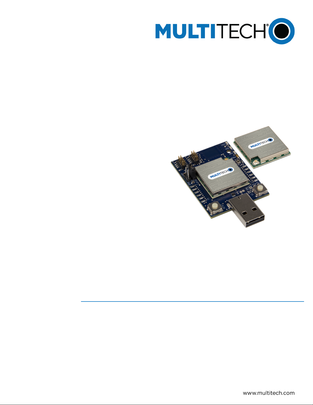
Multi-Tech MultiConnect xDot, MultiConnect xDot MTXDOT-868, MultiConnect xDot MTXDOT-915 Developer's Manual
Page 1
®
MultiConnect
MTXDOT Developer Guide
xDot
TM
Page 2

MULTICONNECT XDOT DEVELOPER GUIDE
MultiConnect xDot Developer Guide
Models: MTXDOT-915-xxx, MTXDOT-868-xxx
Part Number: S000645, Version 1.0
Copyright
This publication may not be reproduced, in whole or in part, without the specific and express prior written permission signed by an executive officer of
Multi-Tech Systems, Inc. All rights reserved. Copyright © 2016 by Multi-Tech Systems, Inc.
Multi-Tech Systems, Inc. makes no representations or warranties, whether express, implied or by estoppels, with respect to the content, information,
material and recommendations herein and specifically disclaims any implied warranties of merchantability, fitness for any particular purpose and noninfringement.
Multi-Tech Systems, Inc. reserves the right to revise this publication and to make changes from time to time in the content hereof without obligation of
Multi-Tech Systems, Inc. to notify any person or organization of such revisions or changes.
Trademarks and Registered Trademarks
MultiTech, and the MultiTech logo, and MultiConnect are registered trademarks and xDot and Conduit are trademarks of Multi-Tech Systems, Inc. All other
products and technologies are the trademarks or registered trademarks of their respective holders.
Legal Notices
The MultiTech products are not designed, manufactured or intended for use, and should not be used, or sold or re-sold for use, in connection with
applications requiring fail-safe performance or in applications where the failure of the products would reasonably be expected to result in personal injury or
death, significant property damage, or serious physical or environmental damage. Examples of such use include life support machines or other life
preserving medical devices or systems, air traffic control or aircraft navigation or communications systems, control equipment for nuclear facilities, or
missile, nuclear, biological or chemical weapons or other military applications (“Restricted Applications”). Use of the products in such Restricted
Applications is at the user’s sole risk and liability.
MULTITECH DOES NOT WARRANT THAT THE TRANSMISSION OF DATA BY A PRODUCT OVER A CELLULAR COMMUNICATIONS NETWORK WILL BE
UNINTERRUPTED, TIMELY, SECURE OR ERROR FREE, NOR DOES MULTITECH WARRANT ANY CONNECTION OR ACCESSIBILITY TO ANY CELLULAR
COMMUNICATIONS NETWORK. MULTITECH WILL HAVE NO LIABILITY FOR ANY LOSSES, DAMAGES, OBLIGATIONS, PENALTIES, DEFICIENCIES, LIABILITIES,
COSTS OR EXPENSES (INCLUDING WITHOUT LIMITATION REASONABLE ATTORNEYS FEES) RELATED TO TEMPORARY INABILITY TO ACCESS A CELLULAR
COMMUNICATIONS NETWORK USING THE PRODUCTS.
The MultiTech products and the final application of the MultiTech products should be thoroughly tested to ensure the functionality of the MultiTech
products as used in the final application. The designer, manufacturer and reseller has the sole responsibility of ensuring that any end user product into
which the MultiTech product is integrated operates as intended and meets its requirements or the requirements of its direct or indirect customers.
MultiTech has no responsibility whatsoever for the integration, configuration, testing, validation, verification, installation, upgrade, support or maintenance
of such end user product, or for any liabilities, damages, costs or expenses associated therewith, except to the extent agreed upon in a signed written
document. To the extent MultiTech provides any comments or suggested changes related to the application of its products, such comments or suggested
changes is performed only as a courtesy and without any representation or warranty whatsoever.
Contacting MultiTech
Knowledge Base
The Knowledge Base provides immediate access to support information and resolutions for all MultiTech products. Visit http://www.multitech.com/kb.go.
Support Portal
To create an account and submit a support case directly to our technical support team, visit: https://support.multitech.com.
Support
Business Hours: M-F, 8am to 5pm CT
Country By Email By Phone
Europe, Middle East, Africa: support@multitech.co.uk +(44) 118 959 7774
U.S., Canada, all others: support@multitech.com (800) 972-2439 or (763) 717-5863
Warranty
To read the warranty statement for your product, visit www.multitech.com/warranty.go. For other warranty options, visit www.multitech.com/es.go.
World Headquarters
Multi-Tech Systems, Inc.
2205 Woodale Drive, Mounds View, MN 55112
Phone: (800) 328-9717 or (763) 785-3500
Fax (763) 785-9874
2 MultiConnect®xDotTMMTXDOT Developer Guide
Page 3

CONTENTS
Contents
Chapter 1 Product Overview .................................................................................................................................... 6
Overview ....................................................................................................................................................................... 6
Documentation Overview ............................................................................................................................................. 6
Related Documentation .............................................................................................................................................. 6
mbed Documentation ................................................................................................................................................... 6
Programming the xDot Microcontroller ..................................................................................................................... 7
General mBed Links .................................................................................................................................................... 7
xDot Platform ............................................................................................................................................................. 7
EUI and Networking ...................................................................................................................................................... 7
Product Build Options ................................................................................................................................................... 8
Chapter 2 Getting Started ........................................................................................................................................ 9
Getting Started with the xDot Developer Kit ................................................................................................................ 9
COM Port Enumeration by Operating System .............................................................................................................. 9
Linux............................................................................................................................................................................ 9
Windows ..................................................................................................................................................................... 9
Mac ........................................................................................................................................................................... 10
Chapter 3 Mechanical Drawings with Pinouts ........................................................................................................ 11
xDot............................................................................................................................................................................. 11
Chapter 4 Specifications and Pin Information ........................................................................................................ 12
MTXDOT Specifications ............................................................................................................................................... 12
Mapping Data Rate to Spreading Factor/Bandwidth................................................................................................ 14
Power Draw................................................................................................................................................................. 15
Measuring the Power Draw ...................................................................................................................................... 15
Electrical Characteristics ............................................................................................................................................. 16
xDot and Processor Pin Information .......................................................................................................................... 16
Pin Information ......................................................................................................................................................... 16
Pull-Up/Down............................................................................................................................................................ 19
xDot Pinout Design Notes ........................................................................................................................................... 20
Serial Pinout Notes.................................................................................................................................................... 20
Serial Settings.............................................................................................................................................................. 20
LoRa ............................................................................................................................................................................ 20
Throughput Rates...................................................................................................................................................... 20
Range ........................................................................................................................................................................ 20
Chapter 5 Antennas ............................................................................................................................................... 22
Antenna System ......................................................................................................................................................... 22
U.FL and Trace Antenna Options ............................................................................................................................... 22
Ethertronics Chip Antenna.......................................................................................................................................... 24
MultiConnect®xDotTMMTXDOT Developer Guide 3
Page 4

CONTENTS
Antenna Specifications ............................................................................................................................................. 24
Pulse Electronics Antenna........................................................................................................................................... 24
Antenna Specifications ............................................................................................................................................. 24
RSMA-to-U.FL Coaxial Cables ..................................................................................................................................... 25
Coaxial Cable Specifications ..................................................................................................................................... 25
OEM Integration ......................................................................................................................................................... 25
FCC & IC Information to Consumers ......................................................................................................................... 25
FCC Grant Notes........................................................................................................................................................ 25
Host Labeling............................................................................................................................................................. 26
Chapter 6 Safety Information................................................................................................................................. 27
Handling Precautions .................................................................................................................................................. 27
Radio Frequency (RF) Safety ....................................................................................................................................... 27
Sécurité relative aux appareils à radiofréquence (RF).............................................................................................. 27
Interference with Pacemakers and Other Medical Devices ...................................................................................... 28
Potential interference............................................................................................................................................... 28
Precautions for pacemaker wearers ........................................................................................................................ 28
Device Maintenance ................................................................................................................................................... 28
User Responsibility...................................................................................................................................................... 28
Chapter 7 Regulatory Information ......................................................................................................................... 29
EMC, Safety, and R&TTE Directive Compliance ......................................................................................................... 29
47 CFR Part 15 Regulation Class B Devices ................................................................................................................. 29
FCC Interference Notice ............................................................................................................................................. 29
FCC Notice................................................................................................................................................................... 29
Industry Canada Class B Notice................................................................................................................................... 30
Chapter 8 Environmental Notices........................................................................................................................... 31
Waste Electrical and Electronic Equipment Statement .............................................................................................. 31
WEEE Directive.......................................................................................................................................................... 31
Instructions for Disposal of WEEE by Users in the European Union ........................................................................ 31
REACH Statement ....................................................................................................................................................... 32
Registration of Substances........................................................................................................................................ 32
Substances of Very High Concern (SVHC) ................................................................................................................ 32
Restriction of the Use of Hazardous Substances (RoHS) ............................................................................................ 33
Information on HS/TS Substances According to Chinese Standards ......................................................................... 34
Information on HS/TS Substances According to Chinese Standards (in Chinese) ...................................................... 35
Chapter 9 Labels .................................................................................................................................................... 36
Label Examples............................................................................................................................................................ 36
Chapter 10 Developer Kit Overview ....................................................................................................................... 37
xDot Developer Kit ..................................................................................................................................................... 37
Developer Kit Package Contents ............................................................................................................................... 37
Firmware Updates..................................................................................................................................................... 37
4 MultiConnect®xDotTMMTXDOT Developer Guide
Page 5

CONTENTS
Programming Devices in Production ........................................................................................................................ 37
xDot Developer Kit Mechanical Drawings................................................................................................................... 38
Micro Developer Board LEDs ...................................................................................................................................... 39
Chapter 11 Developer Board Schematics................................................................................................................ 40
Assembly Diagrams and Schematics ........................................................................................................................... 40
Assembly Diagrams ................................................................................................................................................... 40
Schematics ................................................................................................................................................................ 42
Chapter 12 Design Considerations.......................................................................................................................... 46
Noise Suppression Design ........................................................................................................................................... 46
PC Board Layout Guideline ......................................................................................................................................... 46
Electromagnetic Interference .................................................................................................................................... 46
Electrostatic Discharge Control................................................................................................................................... 47
Chapter 13 Mounting xDots and Programming External Targets ............................................................................ 48
Mounting the Device on Your Board .......................................................................................................................... 48
Solder Profile............................................................................................................................................................... 48
Setpoints (Celsius)..................................................................................................................................................... 49
xDot Packing ............................................................................................................................................................... 49
Programming External Targets ................................................................................................................................... 49
JTAG/SWD Connector .............................................................................................................................................. 50
Index...................................................................................................................................................................... 52
MultiConnect®xDotTMMTXDOT Developer Guide 5
Page 6

CHAPTER 1 PRODUCT OVERVIEW
Chapter 1 Product Overview
Overview
The MultiConnect xDot (MTXDOT) is a LoRaWANTM, low-power RF device, capable of two way communication over
long distances, deep into buildings, or within noisy environments*using the unlicensed ISM bands in North
America, Europe and worldwide. The xDot is a compact surface-mount device with an mbed enabled processor and
enhanced security. The xDot features an integrated ARM®Cortex®-M3 processor and mbedTMcompatible software
library for developers to control, monitor and bring edge intelligence to their Internet of Things (IoT) applications.
*
Actual distance depends on conditions, configuration, antennas, desired throughput, and usage frequency. In
dense urban environments, a typical range is 1-2 miles.
Documentation Overview
This manual is one part of xDot documentation. Refer to the Related Documentation and mbed sections for
additional information needed to program your xDot and integrate your application with the MultiConnect Conduit
gateway.
This document includes:
■ xDot device information: including mechanical drawings, specifications, safety and regulatory information,
and other device specific content.
■ Developer Kit information: including design considerations, schematics, and installation and operation
information.
This current version of this manual is available at www.multitech.com/support.
Related Documentation
■ DOT Series AT Command Reference: Includes details on the AT commands available for xDots.
■ MultiTech Developer Site: Application notes, LoRa information, and documentation for related products
such as the MultiConnect Conduit (MTCDT) gateway and the LoRa accessory card (MTAC-LORA) are available
on the MultiTech developer site. This site includes information on using the Conduit with xDots. Go to:
www.multitech.net
■ Processor Datasheet: ST ARM®Cortex®-M3 processor (STM32L151CCU6) datasheet is available on the ST
website: http://www.st.com/resource/en/datasheet/stm32l151cc.pdf
mbed Documentation
ARM mbed is a free, open-source platform and operating system for embedded devices using the ARM Cortex-M
microcontrollers. The mbed website provides free software libraries, hardware designs, and online tools for rapid
prototyping of products. The platform includes a standards-based C/C++ SDK, a microcontroller HDK, and
supported development boards, an online compiler and online developer collaboration tools.
Note: To send and receive data, you need a LoRaWAN 1.0 gateway, such as MultiTech's MultiConnect Conduit
(MTCDT) with an MTAC-LORA accessory card installed.
6 MultiConnect®xDotTMMTXDOT Developer Guide
Page 7

CHAPTER 1 PRODUCT OVERVIEW
Programming the xDot Microcontroller
Note: To program an xDot application, you need the xDot Developer kit, which includes an xDot mounted on a
developer board.
Use the ARM mbed ecosystem to program the microcontroller. Compile in the cloud or locally, copy the resulting
binary file to the mbed USB drive, and reset the xDot.
On the xDot mbed page, MultiTech supplies source code for non-RF portions of the xDot. To comply with FCC and
ETSI certification, some portions of the software is available only as binary libraries.
MultiTech offers both development and stable release versions of the library.
■ Development version: libmxDot-dev-mbed5
■ Stable release version: libmxDot-mbed5
You can use either the mbed online compiler or offline tools.
■ Online: Use the mbed-os library in your mbed application
■ Offline: Use mbed-cli tools to create, manage, and build your mbed 5.1 application.
General mBed Links
■ Explore mbed: http://developer.mbed.org/explore
■ Getting Started with mbed: http://developer.mbed.org/getting-started
■ mbed Handbook: http://developer.mbed.org/handbook/Homepage
■ mbed online compiler documentation: https://developer.mbed.org/handbook/mbed-Compiler
■ mbed cli documentation: https://github.com/ARMmbed/mbed-cli/blob/master/README.md
■ mbed workspace tools documentation: https://github.com/ARMmbed/mbed-
os/blob/master/docs/BUILDING.md#workspace-tools
xDot Platform
The xDot mbed page includes the xDot library, firmware, and test cases
https://developer.mbed.org/platforms/MTS-xDot-L151CC/
EUI and Networking
xDots have an Extended Unique Identifier (EUI). To query the device for the EUI, AT+DI:
AT+DI=<8-BYTE-HEX-MSB>
AT+DI=001122AABBCCDDEE
For information on setting up xDots as part of a LoRa network, go to www.multitech.net.
MultiConnect®xDotTMMTXDOT Developer Guide 7
Page 8
CHAPTER 1 PRODUCT OVERVIEW
Product Build Options
Product Description Package Quantity
North America
MTXDOT-NA1-A00 915 MHz LoRa Module UFL/TRC (NAM) 1 or 100
MTXDOT-NA1-A01 915 MHz LoRa Module TRC (NAM) 100
EMEA
MTXDOT-EU1-A00 868 MHz LoRa Module UFL/TRC (EU) 1 or 100
MTXDOT-EU1-A01 868 MHz LoRa Module TRC (EU) 100
Developer Kits
MTMDK-XDOT-NA1-A00 MultiConnect xDot Micro Developer Kit - Includes a 915 MHz xDot
MTMDK-XDOT-EU1-A00 MultiConnect xDot Micro Developer Kit - Includes a 868 MHz xDot
Note:
■ The complete product code may end in .Rx. For example, MTXDOT-NA1-A00.Rx, where R is revision
and x is the revision number.
8 MultiConnect®xDotTMMTXDOT Developer Guide
Page 9

CHAPTER 2 GETTING STARTED
Chapter 2 Getting Started
Getting Started with the xDot Developer Kit
Getting started depends on what you want to do. By default, xDot ships with firmware that supports AT
Commands that use the serial I/O. For AT Commands, refer to the separate MultiConnect Dots AT Command
Reference Guide.
Two serial interfaces are available through the USB interface, one is used to send AT commands to the xDot and
the other is for debug messages. Refer to Chapter 4, Specifications and Pin Information for information on which
pins are available out of the box.
Before starting your project development, make sure you have the latest firmware for the Developer Kit and xDot.
Go to the xDot mbed page for firmware. https://developer.mbed.org/platforms/MTS-xDot-L151CC/
To send commands to the xDot:
1. Plug the developer board into a USB port.
2. Open communications software, such as TeraTerm, Putty, or Minicom.
3. Set the following:
■ Baud rate = 115,200
■ Data bits = 8
■ Parity = N
■ Stop bits = 1
■ Flow control = Off
To develop using mbed, the xDot mbed page includes libraries and test cases. Refer to mbed Documentation for
details and links.
For help setting up a MultiConnect®Conduit™to send data to and from an xDot, refer to Related Documentation .
COM Port Enumeration by Operating System
xDots create an AT Commands port and a debug port.
Linux
The following COM ports are created on Linux systems:
■ /dev/ttyACMx
■ /dev/ttyACMy
Where x and y may be 0 and 1, 3 and 4, etc.
The COM port with lower number is the AT command port and COM port with the higher number is the debug
port.
Windows
On Windows systems, COM ports appear in the Device Manager:
■ Debug Port: mbed Serial Port
MultiConnect®xDotTMMTXDOT Developer Guide 9
Page 10

CHAPTER 2 GETTING STARTED
■ AT Command Port: XR21V1410 USB UART
You may need to install a driver for the debug port to function properly. Go to:
https://developer.mbed.org/handbook/Windows-serial-configuration
Mac
On Mac systems, COM ports appear in the Device Manager as:
■ /dev/cu.usbmodemx
Where x is a string of numbers and possibly letters, ending in a number.
The COM port with lower number is the AT command port and COM port with the higher number is the debug
port.
10 MultiConnect®xDotTMMTXDOT Developer Guide
Page 11
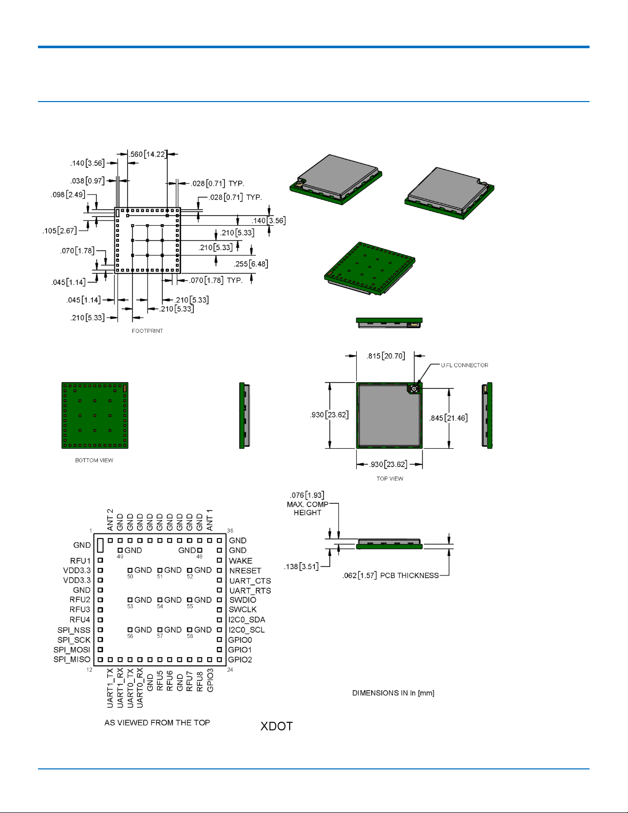
CHAPTER 3 MECHANICAL DRAWINGS WITH PINOUTS
Chapter 3 Mechanical Drawings with Pinouts
xDot
MultiConnect®xDotTMMTXDOT Developer Guide 11
Page 12
CHAPTER 4 SPECIFICATIONS AND PIN INFORMATION
Chapter 4 Specifications and Pin Information
MTXDOT Specifications
Category Description
General
Compatibility LoRaWAN 1.0 specifications
Interfaces Note that pin functions are multiplexed.
Up to 19 digital I/O
Up to 10 analog inputs
2 DAC outputs
I2C
SPI
Wake pin
Reset pin
Full UART
mbed/simple UART (RX & TX only)
mbed programming interface
CPU Performance
CPU 32 MHz
Max Clock 32 MHz
Flash Memory 256 KB, with xDot library 136 KB available; with AT firmware, 56 KB available
EEPROM 8 KB, available 6 KB
SRAM 32 KB
Backup Register 128 byte, available 88
Radio Frequency
ISM Bands 863 MHz - 868 MHz, 902 MHz - 928 MHz, 915 MHz - 935 MHz
Physical Description
Weight 0.0001 oz. (0.003g)
Dimensions Refer to Mechanical Drawings for Dimensions.
RF Connectors
-UFL Models U.FL
-Trace Models Trace Connection
12 MultiConnect®xDotTMMTXDOT Developer Guide
Page 13
Category Description
Environment
CHAPTER 4 SPECIFICATIONS AND PIN INFORMATION
Operating
-40° C to +85° C
Temperature
Storage
-40° C to +85° C
Temperature
Humidity 20%-90% RH, non-condensing
Power Requirements
Operating Voltage 2.4 to 3.57 V
Certifications and Compliance
EMC and Radio
Compliance
EN 300 220-2 V2.4.1:2012 EN 300 220-2 V2.4.1:2012
EN 301 489-03 V1.6.1:2013 ICES-003:2012
FCC 15.247:2015 CISPR 22:2008
FCC 15.109:2015 AS/NZS CISPR 22
FCC 15.107:2015 AS/NZS 4268:2012 + a1:2013
RSS 247:2015 Standard 2014 MPE
Safety Compliance UL 60950-1 2nd ED
cUL 60950-1 2nd ED
IEC 60950-1 2nd ED AM1 + AM2
AS/NZS 60950.1:2015
Category Description
Transmission
North America EMEA
Max Transmitter
19 dBm 14 dBm
Power Output (TPO)
Maximum Receive
-137 dBm -137 dBm
Sensitivity
Link Budget
Max Effective
1
147 dB Point-to-Point 147 dB Point-to-Point
22 dBm 10 dBm
Isotropic Radiated
Power (EiRP)
MultiConnect®xDotTMMTXDOT Developer Guide 13
Page 14

CHAPTER 4 SPECIFICATIONS AND PIN INFORMATION
Category Description
Receive Sensitivity
Spreading Factor North America Typical Sensitivity
2
EMEA Typical Sensitivity
3
6 -111 dBm -121 dBm
7 -116 dBm -124 dBm
8 -119 dBm -127 dBm
9 -122 dBm -130 dBm
10 -125 dBm -133 dBm
11 -127 dBm -135 dBm
12 -129 dBm -137 dBm
1
Greater link budget is possible with higher gain antenna.
2
RFS_L500: RF sensitivity, Long-Range Mode, highest LNA gain, LNA boost, 500 kHz bandwidth using split Rx/Tx
path.
3
RFS_L125: RF sensitivity, Long-Range Mode, highest LNA gain, LNA boost, 125 kHz bandwidth using split Rx/Tx
path.
Mapping Data Rate to Spreading Factor/Bandwidth
Uplink Downlink
US/AU DR0: SF10BW125 DR8: SF12BW500
DR1: SF9BW125 DR9: SF11BW500
DR2: SF8BW125 ...
DR3: SF7BW125 DR13: SF7BW500
DR4: SF8BW500
DR5-DR7: RFU
EU DR0: SF12BW125
...
DR5: SF7BW15
DR6: SF7BW250
DR7: FSK
14 MultiConnect®xDotTMMTXDOT Developer Guide
Page 15
Power Draw
Note:
■ Multi-Tech Systems, Inc. recommends that you incorporate a 10% buffer into the power source
when determining product load.
■ Power measurements are similar for 868 MHz models. Some 868 MHz sub-band frequencies do not
support maximum TXP power of 20.
■ Transmit power measured with MTXDOT-915-xx transmitting to a MultiConnect Conduit with an
MTAC-LORA-915 accessory card installed.
■ Idle current measured with the xDot joined with Conduit, but idle without data transferring.
■ Transmit power measured while transferring data packets using spread factor 9. Packet size limited
to 53 bytes. The Conduit was set to receive packets from and send back to the xDot. A script was run
to send the packet 100 times with either 10 or 53 bytes of data, with an average measurement taken
during that time.
■ For Inrush charge, recorded the highest observed value from five separate measurements.
CHAPTER 4 SPECIFICATIONS AND PIN INFORMATION
Voltage USB = 5v Standby Mode
Current, (Sleep = 0
Deep Sleep)
LDO = 3.3 1.9uA 2.2uA 11.1mA DR1 - SF9BW125 10
LDO = 3.3 1.9uA 2.2uA 11.1mA DR1 - SF9BW125 53
Voltage USB =5vAverage Current
(Amps) at Low
Transmit Power
Setting (TXP 2)
LDO = 3.3 0.013 0.017 0.018 0.132mC 153uS
LDO = 3.3 0.017 0.024 0.025 0.132mC 147uS
Average Current
(Amps) at Default
Transmit Power
Setting (TXP 11)
Stop Mode
Current,
(Sleep = 1)
Idle current
Average
Average Current
(Amps) at
Maximum
Transmit Power
Setting (TXP 20)
Spreading Factor Setting Packet Size (#
Total Inrush
Charge
measured in
MilliCoulombs
Total Inrush Charge
DURATION during
Powerup (INRUSH
Duration)
Measuring the Power Draw
To measure the power draw on an xDot developer board:
1. Flash the latest AT command firmware on the xDot.
2. Unplug the xDot from the computer and then reconnect it.
3. Connect current meter across JP30 on the developer board.
4. Set wake pin to wake, AT+WP=6.
5. Set wake mode to interrupt, AT+WM=1.
6. Put the xDot to sleep, AT+SLEEP=0|1.
7. Put jumper across JP5.
Bytes)
Note: After this step, AT command and debug ports no longer work.
8. Measure current draw.
9. Press the S2 button on the developer board to wake the xDot
MultiConnect®xDotTMMTXDOT Developer Guide 15
Page 16
CHAPTER 4 SPECIFICATIONS AND PIN INFORMATION
Electrical Characteristics
Signal Description Min Max
Vin Low Input low level -- 0.3 * VDD
Vin High Input high level 0.45 * VDD +0.6 --
Vout Low Output low level -- .4
Vout High Output high level 0.4 --
VCC Standard operating voltage 2.4 3.6
ICC Operating current (mA)
@5V
Operating current (mA)
@3.3V
xDot and Processor Pin Information
-- 135
-- 200
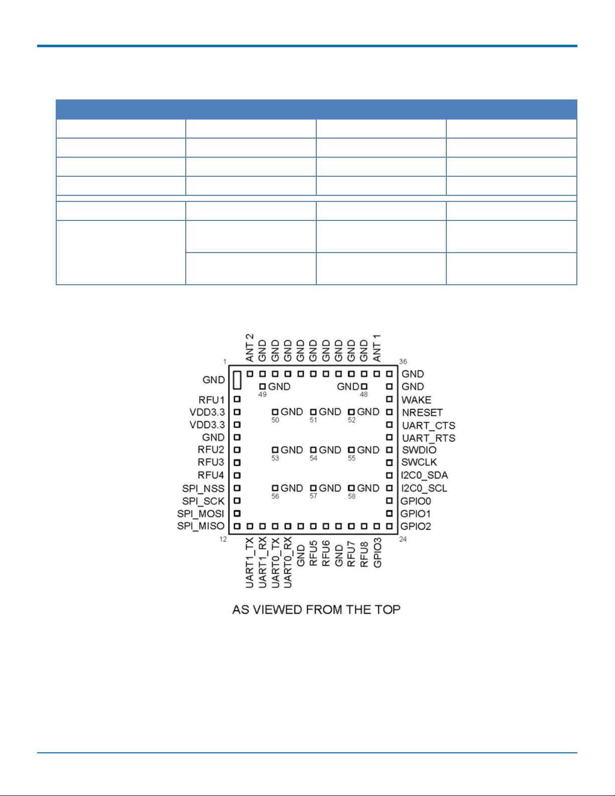
Pin Information
Note:
■ Using the mbed platform expands your pin functionality options.
■ Pins are on a 0.07 inch grid, and are 0.028 inches square (except for upper left)
■ The xDot is 0.045 x 0.045, board is 0.93 x 0.93
16 MultiConnect®xDotTMMTXDOT Developer Guide
Page 17

CHAPTER 4 SPECIFICATIONS AND PIN INFORMATION
48QFN xDot Pin Pin Name SW Name Function
Description
Processor Pin
Alt1
25 9 PB12 SPI2_NSS GPIO / SPI TIM10_CH1/
I2C2_SMBA/
SPI2_NSS/
I2S2_WS/
USART3_CK/
LCD_SEG12
26 10 PB13 SPI2_SCK GPIO / SPI TIM9_CH1/
SPI2_SCK/
I2S2_CK/
USART3_CTS/
LCD_SEG13
28 11 PB15 SPI2_MOSI GPIO / SPI TIM11_CH1/
SPI2_MOSI/
I2S2_SD/
LCD_SEG15
27 12 PB14 SPI2_MISO GPIO / SPI TIM9_CH2/
SPI2_MISO/
USART3_RTS/
LCD_SEG14
Processor Pin Alt2
ADC_IN18/
COMP1_INP/
VLCDRAIL2
ADC_IN19/
COMP1_INP
ADC_IN21/
COMP1_INP/
RTC_REFIN
ADC_IN20/
COMP1_INP
30 13 PA9 UART1_TX GPIO / UART USART1_TX/
-
LCD_COM1
31 14 PA10 UART1_RX GPIO / UART USART1_RX/
-
LCD_COM2
12 15 PA2 UART2_TX Debug UART
13 16 PA3 UART2_RX Debug UART
20 23 PB2 GPIO3 GPIO BOOT1 VLCDRAIL1/ ADCIN0b
18 24 PB0 GPIO2 GPIO TIM3_CH3/
LCD_SEG5
ADC_IN8/
COMP1_INP/
OPAMP2_VOUT/
VLCDRAIL3/
VREF_OUT
15 25 PA5 GPIO1 GPIO TIM2_CH1_ETR/
SPI1_SCK
ADC_IN5/
DAC_OUT2/
COMP1_INP
14 26 PA4 GPIO0 GPIO SPI1_NSS/
SPI3_NSS/
I2S3_WS/
ADC_IN4/
DAC_OUT1/
COMP1_INP
USART2_CK
45 27 PB8 I2C1_SCL GPIO / I2C TIM4_CH3/
TIM10_CH1/
I2C1_SCL/
LCD_SEG16
MultiConnect®xDotTMMTXDOT Developer Guide 17
Page 18

CHAPTER 4 SPECIFICATIONS AND PIN INFORMATION
48QFN xDot Pin Pin Name SW Name Function
Description
Processor Pin
Alt1
46 28 PB9 I2C1_SDA GPIO / I2C TIM4_CH4/
TIM11_CH1/
I2C1_SDA/
LCD_COM3
37 29 PA14 MBED SWCLK JTCK-SWCLK -
34 30 PA13 MBED SWDIO JTMS-SWDIO -
33 31 PA12 UART1_RTS GPIO / UART USART1_RTS/
SPI1_MOSI
32 32 PA11 UART1_CTS GPIO / UART USART1_CTS/
SPI1_MISO
7 33 NRST NRESET - -
10 34 PA0-WKUP1 WAKE GPIO / WAKE TIM2_CH1_ETR/
TIM5_CH1/
USART2_CTS
37 ANT1
47 RFU (ANT2)
Processor Pin Alt2
-
USB_DP
USB_DM
WKUP1/
RTC_TAMP2/
ADC_IN0/
COMP1_INP
8,23,35
,47,49
1, 5, 17,
20,35, 36,
VSS GND
38, 39,
40, 41,
42, 43,
44, 45,
46, 48,
49, 50,
51, 52,
53, 54,
55, 56,
57, 58
2, 6, 7, 8,
Reserved
18, 19,
21, 22
16 PA6 LORA_DIO0 LORA Radio
17 PA7 LORA_DIO1 LORA Radio
29 PA8 LORA_DIO2 LORA Radio
42 PB6 LORA_DIO3 LORA Radio
43 PB7 LORA_DIO4 LORA Radio
40 PB4 LORA_MISO LORA Radio
41 PB5 LORA_MOSI LORA Radio
18 MultiConnect®xDotTMMTXDOT Developer Guide
Page 19

CHAPTER 4 SPECIFICATIONS AND PIN INFORMATION
48QFN xDot Pin Pin Name SW Name Function
Description
38 PA15 LORA_NSS LORA Radio
11 PA1 LORA_RESET LORA Radio
39 PB3 LORA_SCK LORA Radio
22 PB11 SE_CLK Secure Element
19 PB1 SE_CTRL Secure Element
21 PB10 SE_IO Secure Element
2 PC13-WKUP2 SE_RESET Secure Element
44 BOOT0 Boot0 - -
3 PC14-
OSC32_IN(4)
4 PC15-
OSC32_OUT
5 PH0-
OSC_IN(5)
6 PH1-
OSC_OUT(5)
RTC_CLK - OSC32_IN
RTC_CLK - OSC32_OUT
Main 24M - OSC_IN
Main 24M - OSC_OUT
Processor Pin
Alt1
Processor Pin Alt2
Pull-Up/Down
48QFN xDot Pin Pin Name SW Name PU/PD
7 33 NRST 10k PU
38 PA15 LORA_NSS 100k PU
19 PB1 SE_CTRL 10k PU
44 BOOT0 10k PD
MultiConnect®xDotTMMTXDOT Developer Guide 19
Page 20

CHAPTER 4 SPECIFICATIONS AND PIN INFORMATION
xDot Pinout Design Notes
Refer to the mechanical drawing for your model for pin locations.
■ All pins that go to connectors are directly connected to the processor.
■ Refer to Pin Information table for pull up and pull down information.
xDots allow you to program pins depending on your application:
■ Serial: Available out of the box. See Serial Pinout Notes for details.
■ mbed: Designed with the STM32L151CCU6 48-pin processor, this option provides the most flexibility. For
more information about processor capabilities, see the processor datasheet.
Serial Pinout Notes
Out of the box, these pins are available for serial applications. Refer to the mechanical drawing for your model for
pin locations.
■ 18 PTA1 UART1_CTS
■ 19 PTA2 UART1_RTS
■ 36 PTC3 UART1_RX
■ 37 PTC4 UART1_TX
Serial Settings
When creating a serial connection with the device on the developer board, open communications software (such
as TeraTerm, Putty, or Minicom ), and use the following settings:
■ Baud rate = 115,200
■ Data bits = 8
■ Parity = N
■ Stop bits = 1
■ Flow control = Off
LoRa
Throughput Rates
Theoretical maximum speeds for LoRa mode with ACKs off are:
■ Using spreading factor 7 at 125kHz, the throughput rate is 5470 bps (5.47 kbps).
■ Using spreading factor 7 at 500kHz the receiving throughput rate is 21900 bps (21.9 kbps).
Note: Data rates in the LoRaWAN specification vary by geographic region.
Range
Variables effecting the range include TX power, antenna gain, RX sensitivity, fade margin, earth's curvature. Use
the following formula to calculate the maximum range:
20 MultiConnect®xDotTMMTXDOT Developer Guide
Page 21

CHAPTER 4 SPECIFICATIONS AND PIN INFORMATION
The following table provides example settings and the theoretical maximum range based on these settings.
Example 18dB Transmit Power for
915 MHz Models
Units Example 14dB Transmit Power for
868MHz Models
Frequency 915 MHz 868
TX Power 19 dBm 14
TX Antenna Gain 3 dB 3
RX Sensitivity
1
-120 dBm -120
RX Antenna Gain 3 dB 3
Fade Margin
2
30 dB 30
Distance 8.14 Miles 5.41
Distance 13.08 Km 8.70
1
RX Sensitivity is set to a conservative -120dBm, but can vary from -117 to -137dBm.
2
Fade Margin is set at the worst case of 30dB. Fade margin is an allowance a system designer includes to account
for unknown variables. The higher the fade margin, the better the overall link quality will be. With a fade margin
set to zero, the link budget is still valid, but only in LOS conditions, which is not practical for most designs. The
amount of fade margin to include in a calculation depends on the environment in which you will deploy the
system. A fade margin of 12 dBm is good, but a better number would be 20 to 30 dBm.
MultiConnect®xDotTMMTXDOT Developer Guide 21
Page 22

CHAPTER 5 ANTENNAS
Chapter 5 Antennas
Antenna System
The LoRa antenna performance depends on the implementation and antenna design. The integration of the
antenna system into the product is a critical part of the design process; therefore, it is essential to consider it early
so the performance is not compromised. If changes are made to the device's certified antenna system, then
recertification will be required.
This radio transmitter has been approved with the antenna types listed below. The antenna used must maintain
the same specifications. The antenna must be of the same type, with similar in-band and out-of-band radiation
patterns. Antenna types not included on this list, or having a greater gain than the maximum gain indicated for the
listed type, are strictly prohibited for use with this device.
U.FL and Trace Antenna Options
If using U.FL or trace antennas, note the following:
■ For a simple trace to RF antennas: Routing must follow standard RF design rules and practices for
stripline/miscrostrip for a 50 ohm impedance line. Use the developer board schematics for a reference
circuit for the a trace antenna.
■ For U.FL antennas: The antenna and cable combination in your design cannot exceed the performance of
the SMA antenna as listed in the next topic.
■ The xDot Developer Board includes an Ethertronics M6200710-1K chip antenna, which by default connects
the xDot to the chip antenna. Only one antenna, either U.FL or chip, may be used at a time. To use the
xDot’s U.FL connector, remove resistor C23 and L1, marked on the following image, to disconnect the chip
antenna.
■ If using a chip antenna in your design, consult your antenna's documentation for placement and design
guidelines.
22 MultiConnect®xDotTMMTXDOT Developer Guide
Page 23

CHAPTER 5 ANTENNAS
MultiConnect®xDotTMMTXDOT Developer Guide 23
Page 24

CHAPTER 5 ANTENNAS
Ethertronics Chip Antenna
This is the developer board's default antenna.
Manufacturer: Ethertronics
Description: 915MHz Chip RF Antenna 902MHz ~ 928MHz 2.56dB Solder Surface Mount
Model Number: M620710-1K
Antenna Specifications
Category Description
Electrical Specifications
Frequency Range 902—928 MHz
Peak Gain 2.56 dBi
VSWR 2:6:1 max
Impedance 50 ohms unbalanced
Average Efficiency 58%
Power Handling 0.5 Watt cw
Polarization Linear
Mechanical Specifications
Mounting Surface Mount
Size 6.00 x 2.00 x 1.1mm
Pulse Electronics Antenna
Manufacturer: Pulse Electronics
Description: 868-915 MHz RP-SMA Antenna, 8"
Model Number: W1063
MultiTech Part Number: 45009830L
MultiTech ordering information:
Ordering Part Number Quantity
AN868-915A-1HRA 1
AN868-915A-10HRA 10
AN868-915A-50HRA 50
Antenna Specifications
Category Description
Frequency Range 868-928 MHz
24 MultiConnect®xDotTMMTXDOT Developer Guide
Page 25

Category Description
Impedance 50 Ohms
VSWR < 2.0
Gain 3.0 dBi
Radiation Omni
Polarization Vertical
RSMA-to-U.FL Coaxial Cables
Coaxial Cable Specifications
Optional antenna cables can be ordered from MultiTech
Cable Type Coaxial Cable
Attenuation <1.0db
Connector Impedance 50 ohm
CHAPTER 5 ANTENNAS
Maximum Cable Length 16" (40 cm)
Ordering Information
Part Number Description
CARSMA-UFL-1 RSMA-to-UFL Coax Cable (Single Pack)
CARSMA-UFL-10 RSMA-to-UFL Coax Cable (Ten Pack)
CARSMA-UFL-100 RSMA-to-UFL Coax Cable (One Hundred Pack)
OEM Integration
FCC & IC Information to Consumers
The user manual for the consumer must contain the statements required by the following FCC and IC regulations:
47 C.F.R. 15.19(a)(3), 15.21, 15.105 and RSS-Gen Issue 4 Sections 8.3 and 8.4.
FCC Grant Notes
The OEM should follow all the grant notes listed below. Otherwise, further testing and device approvals may be
necessary.
FCC Definitions
Portable: (§2.1093) — A portable device is defined as a transmitting device designed to be used so that the
radiating structure(s) of the device is/are within 20 centimeters of the body of the user.
Mobile: (§2.1091) — A mobile device is defined as a transmitting device designed to be used in other than fixed
locations and to generally be used in such a way that a separation distance of at least 20 centimeters is normally
maintained between the transmitter’s radiating structure(s) and the body of the user or nearby persons.
MultiConnect®xDotTMMTXDOT Developer Guide 25
Page 26

CHAPTER 5 ANTENNAS
Actual content pending Grant: This device is a mobile device with respect to RF exposure compliance. The
antenna(s) used for this transmitter must be installed to provide a separation distance of at least 20 cm from all
persons, and must not be collocated or operate in conjunction with any other antenna or transmitter except in
accordance with FCC multi-transmitter product guidelines. Installers and end-users must be provided with specific
information required to satisfy RF exposure compliance for installations and final host devices. (See note under
Grant Limitations.) Compliance of this device in all final host configurations is the responsibility of the Grantee.
Note: Host design configurations constituting a device for portable use (<20 cm from human body) require
separate FCC/IC approval.
Host Labeling
The following statements are required to be on the host label:
This device contains FCC ID: {Add the FCC ID of the specific device}
This device contains equipment certified under IC ID: {Add the IC ID of the specific device}
For additional labeling requirements, see the product's Labeling Requirements. For the FCC and IC IDs, see specific
certificate information in the Regulatory Statement chapter.
26 MultiConnect®xDotTMMTXDOT Developer Guide
Page 27

CHAPTER 6 SAFETY INFORMATION
Chapter 6 Safety Information
Handling Precautions
To avoid damage due to the accumulation of static charge, use proper precautions when handling any cellular
device. Although input protection circuitry has been incorporated into the devices to minimize the effect of static
build-up, use proper precautions to avoid exposure to electronic discharge during handling and mounting the
device.
Radio Frequency (RF) Safety
Due to the possibility of radio frequency (RF) interference, it is important that you follow any special regulations
regarding the use of radio equipment. Follow the safety advice given below.
■ Operating your device close to other electronic equipment may cause interference if the equipment is
inadequately protected. Observe any warning signs and manufacturers’ recommendations.
■ Different industries and businesses restrict the use of cellular devices. Respect restrictions on the use of
radio equipment in fuel depots, chemical plants, or where blasting operations are in process. Follow
restrictions for any environment where you operate the device.
■ Do not place the antenna outdoors.
■ Switch OFF your wireless device when in an aircraft. Using portable electronic devices in an aircraft may
endanger aircraft operation, disrupt the cellular network, and is illegal. Failing to observe this restriction
may lead to suspension or denial of cellular services to the offender, legal action, or both.
■ Switch OFF your wireless device when around gasoline or diesel-fuel pumps and before filling your vehicle
with fuel.
■ Switch OFF your wireless device in hospitals and any other place where medical equipment may be in use.
Sécurité relative aux appareils à radiofréquence (RF)
À cause du risque d'interférences de radiofréquence (RF), il est important de respecter toutes les réglementations
spéciales relatives aux équipements radio. Suivez les conseils de sécurit é ci-dessous.
■ Utiliser l'appareil à proximité d'autres équipements électroniques peut causer des interférences si les
équipements ne sont pas bien protégés. Respectez tous les panneaux d'avertissement et les
recommandations du fabricant.
■ Certains secteurs industriels et certaines entreprises limitent l'utilisation des appareils cellulaires. Respectez
ces restrictions relatives aux équipements radio dans les dépôts de carburant, dans les usines de produits
chimiques, ou dans les zones où des dynamitages sont en cours. Suivez les restrictions relatives à chaque
type d'environnement où vous utiliserez l'appareil.
■ Ne placez pas l'antenne en extérieur.
■ Éteignez votre appareil sans fil dans les avions. L'utilisation d'appareils électroniques portables en avion est
illégale: elle peut fortement perturber le fonctionnement de l'appareil et désactiver le réseau cellulaire. S'il
ne respecte pas cette consigne, le responsable peut voir son accès aux services cellulaires suspendu ou
interdit, peut être poursuivi en justice, ou les deux.
■ Éteignez votre appareil sans fil à proximité des pompes à essence ou de diesel avant de remplir le réservoir
de votre véhicule de carburant.
MultiConnect®xDotTMMTXDOT Developer Guide 27
Page 28

CHAPTER 6 SAFETY INFORMATION
■ Éteignez votre appareil sans fil dans les hôpitaux ou dans toutes les zones où des appareils médicaux sont
susceptibles d'être utilisés.
Interference with Pacemakers and Other Medical Devices
Potential interference
Radio frequency energy (RF) from cellular devices can interact with some electronic devices. This is
electromagnetic interference (EMI). The FDA helped develop a detailed test method to measure EMI of implanted
cardiac pacemakers and defibrillators from cellular devices. This test method is part of the Association for the
Advancement of Medical Instrumentation (AAMI) standard. This standard allows manufacturers to ensure that
cardiac pacemakers and defibrillators are safe from cellular device EMI.
The FDA continues to monitor cellular devices for interactions with other medical devices. If harmful interference
occurs, the FDA will assess the interference and work to resolve the problem.
Precautions for pacemaker wearers
If EMI occurs, it could affect a pacemaker in one of three ways:
■ Stop the pacemaker from delivering the stimulating pulses that regulate the heart's rhythm.
■ Cause the pacemaker to deliver the pulses irregularly.
■ Cause the pacemaker to ignore the heart's own rhythm and deliver pulses at a fixed rate.
Based on current research, cellular devices do not pose a significant health problem for most pacemaker wearers.
However, people with pacemakers may want to take simple precautions to be sure that their device doesn't cause
a problem.
■ Keep the device on the opposite side of the body from the pacemaker to add extra distance between
the pacemaker and the device.
■ Avoid placing a turned-on device next to the pacemaker (for example, don’t carry the device in a shirt
or jacket pocket directly over the pacemaker).
Device Maintenance
When maintaining your device:
■ Do not attempt to disassemble the device. There are no user serviceable parts inside.
■ Do not expose your device to any extreme environment where the temperature or humidity is high.
■ Do not expose the device to water, rain, or spilled beverages. It is not waterproof.
■ Do not place the device alongside computer discs, credit or travel cards, or other magnetic media. The
information contained on discs or cards may be affected by the device.
■ Using accessories, such as antennas, that MultiTech has not authorized or that are not compliant with
MultiTech's accessory specifications may invalidate the warranty.
If the device is not working properly, contact MultiTech Technical Support.
User Responsibility
Respect all local regulations for operating your wireless device. Use the security features to block unauthorized use
and theft.
28 MultiConnect®xDotTMMTXDOT Developer Guide
Page 29

CHAPTER 7 REGULATORY INFORMATION
Chapter 7 Regulatory Information
EMC, Safety, and R&TTE Directive Compliance
The CE mark is affixed to this product to confirm compliance with the following European Community Directives:
Council Directive 2014/30/EU on the approximation of the laws of Member States relating to
electromagnetic compatibility;
and
Council Directive 2014/35/EU on the harmonization of the laws of Member States relating to electrical
equipment designed for use within certain voltage limits;
and
Council Directive 2011/65/EU on the restriction of the use of certain hazardous substances in electrical
and electronic equipment;
and
Council Directive 1999/5/EC on radio equipment and telecommunications terminal equipment and the
mutual recognition of their conformity.
47 CFR Part 15 Regulation Class B Devices
This equipment has been tested and found to comply with the limits for a Class B digital device, pursuant to part
15 of the FCC Rules. These limits are designed to provide reasonable protection against harmful interference in a
residential installation. This equipment generates, uses, and can radiate radio frequency energy and, if not installed
and used in accordance with the instructions, may cause harmful interference to radio communications. However,
there is no guarantee that interference will not occur in a particular installation. If this equipment does cause
harmful interference to radio or television reception, which can be determined by turning the equipment off and
on, the user is encouraged to try to correct the interference by one or more of the following measures:
■ Reorient or relocate the receiving antenna.
■ Increase the separation between the equipment and receiver.
■ Connect the equipment into an outlet on a circuit different from that to which the receiver is connected.
■ Consult the dealer or an experienced radio/TV technician for help.
Warning: Changes or modifications to this unit not expressly approved by the party responsible for compliance
could void the user’s authority to operate the equipment.
FCC Interference Notice
Per FCC 15.19(a)(3) and (a)(4) This device complies with part 15 of the FCC Rules. Operation is subject to the
following two conditions: (1) This device may not cause harmful interference, and (2) this device must accept any
interference received, including interference that may cause undesired operation.
FCC Notice
xDot products are open development based products that contain a sub ghz radio technology. MultiTech has
certified for compliance with US and Foreign compliance bodies including FCC, R&TTE and others. (e.g. FCC
15.247:2015 & IC RSS 247:2015)
MultiConnect®xDotTMMTXDOT Developer Guide 29
Page 30

CHAPTER 7 REGULATORY INFORMATION
MultiTech provides software code meant to operate the radio to a level that maintains compliance with the
operating modes under which these radio devices were certified. To ensure this level of compliance, the software
code is provided in binary form only. Users are prohibited from making any changes that affect the operation of
the radio performance. Accessing or controlling the radio through any means other than the provided binary
software will require the user to obtain their own intentional radiator license from the certification body governing
their locality, as all pre-certification provided with xDot will have been made invalid.
Industry Canada Class B Notice
This Class B digital apparatus meets all requirements of the Canadian Interference-Causing Equipment Regulations.
Cet appareil numérique de la classe B respecte toutes les exigences du Reglement Canadien sur le matériel
brouilleur.
This device complies with Industry Canada license-exempt RSS standard(s). The operation is permitted for the
following two conditions:
1. the device may not cause harmful interference, and
2. the user of the device must accept any interference suffered, even if the interference is likely to
jeopardize the operation.
Le présent appareil est conforme aux CNR d'Industrie Canada applicables aux appareils radio exempts de licence.
L'exploitation est autorisée aux deux conditions suivantes:
1. l'appareil ne doit pas produire de brouillage, et
2. l'utilisateur de l'appareil doit accepter tout brouillage radioélectrique subi, m ême si le brouillage est
susceptible d'en compromettre le fonctionnement.
30 MultiConnect®xDotTMMTXDOT Developer Guide
Page 31

CHAPTER 8 ENVIRONMENTAL NOTICES
Chapter 8 Environmental Notices
Waste Electrical and Electronic Equipment Statement
Note: This statement may be used in documentation for your final product applications.
WEEE Directive
The WEEE Directive places an obligation on EU-based manufacturers, distributors, retailers, and importers to takeback electronics products at the end of their useful life. A sister directive, ROHS (Restriction of Hazardous
Substances) complements the WEEE Directive by banning the presence of specific hazardous substances in the
products at the design phase. The WEEE Directive covers all MultiTech products imported into the EU as of August
13, 2005. EU-based manufacturers, distributors, retailers and importers are obliged to finance the costs of recovery
from municipal collection points, reuse, and recycling of specified percentages per the WEEE requirements.
Instructions for Disposal of WEEE by Users in the European Union
The symbol shown below is on the product or on its packaging, which indicates that this product must not be
disposed of with other waste. Instead, it is the user's responsibility to dispose of their waste equipment by handing
it over to a designated collection point for the recycling of waste electrical and electronic equipment. The separate
collection and recycling of your waste equipment at the time of disposal will help to conserve natural resources
and ensure that it is recycled in a manner that protects human health and the environment. For more information
about where you can drop off your waste equipment for recycling, please contact your local city office, your
household waste disposal service or where you purchased the product.
July, 2005
MultiConnect®xDotTMMTXDOT Developer Guide 31
Page 32

CHAPTER 8 ENVIRONMENTAL NOTICES
REACH Statement
Registration of Substances
After careful review of the legislation and specifically the definition of an “article” as defined in EC Regulation
1907/2006, Title II, Chapter 1, Article 7.1(a)(b), it is our current view Multi-Tech Systems, Inc. products would be
considered as “articles”. In light of the definition in § 7.1(b) which requires registration of an article only if it
contains a regulated substance that “is intended to be released under normal or reasonably foreseeable conditions
of use,” Our analysis is that Multi-Tech Systems, Inc. products constitute nonregisterable articles for their intended
and anticipated use.
Substances of Very High Concern (SVHC)
Per the candidate list of Substances of Very High Concern (SVHC) published October 28, 2008 we have reviewed
these substances and certify the Multi-Tech Systems, Inc. products are compliant per the EU “REACH”
requirements of less than 0.1% (w/w) for each substance. If new SVHC candidates are published by the European
Chemicals Agency, and relevant substances have been confirmed, that exceeds greater than 0.1% (w/w), MultiTech Systems, Inc. will provide updated compliance status.
Multi-Tech Systems, Inc. also declares it has been duly diligent in ensuring that the products supplied are compliant
through a formalized process which includes collection and validation of materials declarations and selective
materials analysis where appropriate. This data is controlled as part of a formal quality system and will be made
available upon request.
32 MultiConnect®xDotTMMTXDOT Developer Guide
Page 33

CHAPTER 8 ENVIRONMENTAL NOTICES
Restriction of the Use of Hazardous Substances (RoHS)
Multi-Tech Systems, Inc.
Certificate of Compliance
2011/65/EU
Multi-Tech Systems, Inc. confirms that its embedded products comply with the chemical concentration limitations
set forth in the directive 2011/65/EU of the European Parliament (Restriction of the use of certain Hazardous
Substances in electrical and electronic equipment - RoHS).
These MultiTech products do not contain the following banned chemicals1:
■ Lead, [Pb] < 1000 PPM
■ Mercury, [Hg] < 1000 PPM
■ Hexavalent Chromium, [Cr+6] < 1000 PPM
■ Cadmium, [Cd] < 100 PPM
■ Polybrominated Biphenyl, [PBB] < 1000 PPM
■ Polybrominated Diphenyl Ether, [PBDE] < 1000 PPM
Environmental considerations:
■ Moisture Sensitivity Level (MSL) =1
■ Maximum Soldering temperature = 260C (in SMT reflow oven)
1
Lead usage in some components is exempted by the following RoHS annex, therefore higher lead concentration
would be found in some modules (>1000 PPM);
- Resistors containing lead in a glass or ceramic matrix compound.
MultiConnect®xDotTMMTXDOT Developer Guide 33
Page 34

CHAPTER 8 ENVIRONMENTAL NOTICES
Information on HS/TS Substances According to Chinese Standards
In accordance with China's Administrative Measures on the Control of Pollution Caused by Electronic Information
Products (EIP) # 39, also known as China RoHS, the following information is provided regarding the names and
concentration levels of Toxic Substances (TS) or Hazardous Substances (HS) which may be contained in Multi-Tech
Systems Inc. products relative to the EIP standards set by China's Ministry of Information Industry (MII).
Hazardous/Toxic Substance/Elements
Name of the Component Lead
(PB)
Printed Circuit Boards O O O O O O
Resistors X O O O O O
Capacitors X O O O O O
Ferrite Beads O O O O O O
Relays/Opticals O O O O O O
ICs O O O O O O
Diodes/ Transistors O O O O O O
Oscillators and Crystals X O O O O O
Regulator O O O O O O
Voltage Sensor O O O O O O
Transformer O O O O O O
Speaker O O O O O O
Connectors O O O O O O
Mercury
(Hg)
Cadmium
(CD)
Hexavalent
Chromium
(CR6+)
Polybromi
nated
Biphenyl
(PBB)
Polybrominat
ed Diphenyl
Ether (PBDE)
LEDs O O O O O O
Screws, Nuts, and other
Hardware
AC-DC Power Supplies O O O O O O
Software /Documentation CDs O O O O O O
Booklets and Paperwork O O O O O O
Chassis O O O O O O
X Represents that the concentration of such hazardous/toxic substance in all the units of homogeneous
material of such component is higher than the SJ/Txxx-2006 Requirements for Concentration Limits.
O Represents that no such substances are used or that the concentration is within the aforementioned limits.
34 MultiConnect®xDotTMMTXDOT Developer Guide
X O O O O O
Page 35

CHAPTER 8 ENVIRONMENTAL NOTICES
Information on HS/TS Substances According to Chinese Standards (in Chinese)
依依照照中中国国标标准准的的有有毒毒有有害害物物质质信信息息
根据中华人民共和国信息产业部 (MII) 制定的电子信息产品 (EIP) 标准-中华人民共和国《电子信息产品污染
控制管理办法》(第 39 号),也称作中国 RoHS, 下表列出了 Multi-Tech Systems, Inc. 产品中可能含有的有毒
物质 (TS) 或有害物质 (HS) 的名称及含量水平方面的信息。
有有害害//有有毒毒物物质质//元元素素
成成分分名名称称
印刷电路板
电阻器
电容器
铁氧体磁环
继电器/光学部件
ICs O O O O O O
二极管/晶体管
振荡器和晶振
调节器
电压传感器
变压器
扬声器
连接器
LEDs O O O O O O
铅铅 (PB) 汞汞 (Hg) 镉镉 (CD) 六六价价铬铬 (CR6+)
O O O O O O
X O O O O O
X O O O O O
O O O O O O
O O O O O O
O O O O O O
X O O O O O
O O O O O O
O O O O O O
O O O O O O
O O O O O O
O O O O O O
多多溴溴联联苯苯
(PBB)
多多溴溴二二苯苯醚醚
(PBDE)
螺丝、螺母以及其它五金件
交流-直流电源
软件/文档 CD
手册和纸页
底盘
X 表示所有使用类似材料的设备中有害/有毒物质的含量水平高于 SJ/Txxx-2006 限量要求。
O 表示不含该物质或者该物质的含量水平在上述限量要求之内。
MultiConnect®xDotTMMTXDOT Developer Guide 35
X O O O O O
O O O O O O
O O O O O O
O O O O O O
O O O O O O
Page 36

CHAPTER 9 LABELS
Chapter 9 Labels
Label Examples
Note: Actual labels vary depending on the regulatory approval markings and content.
This device complies with part 15 of the FCC Rules. Operation is subject to the following two conditions: (1) This
device may not cause harmful interference, and (2) this device must accept any interference received, including
interference that may cause undesired operation.
The label shown is not the actual size.
1 - MultiTech Model Identification.
2 - MultiTech Ordering Part Number.
3 - Device Node Number.
Example xDot Device Label Example Developer Board Device Label
36 MultiConnect®xDotTMMTXDOT Developer Guide
Page 37

CHAPTER 10 DEVELOPER KIT OVERVIEW
Chapter 10 Developer Kit Overview
xDot Developer Kit
The xDot developer kit comes with an xDot already mounted on the developer board. Simply plug the developer kit
into a USB port on your computer to test, program, and evaluate your application.
Developer Kit Package Contents
Your Developer Kit (MTMDK-NX-XDOT-xx) includes the following:
Developer Board 1 - xDot Developer Board with xDot
Customer Notices Quick Start
Firmware Updates
Before starting your project development, make sure you have the latest firmware for the Developer Kit and xDot.
Go to the xDot mbed page for firmware. https://developer.mbed.org/platforms/MTS-xDot-L151CC/
Programming Devices in Production
Consult developer kit schematics for programming options.
MultiConnect®xDotTMMTXDOT Developer Guide 37
Page 38

CHAPTER 10 DEVELOPER KIT OVERVIEW
xDot Developer Kit Mechanical Drawings
Note: The Reset and Wake buttons reset and wake the xDot processor.
38 MultiConnect®xDotTMMTXDOT Developer Guide
Page 39

CHAPTER 10 DEVELOPER KIT OVERVIEW
Micro Developer Board LEDs
LED Description
LED1 User-definable LED.
LED3/SDA Programming Status.
LED2/PWR Power, blue light when the board has power.
LED4/PROXY LED for the proximity sensor, which is next to it (labeled U14 on the top assembly
diagram).
MultiConnect®xDotTMMTXDOT Developer Guide 39
Page 40

CHAPTER 11 DEVELOPER BOARD SCHEMATICS
Chapter 11 Developer Board Schematics
Assembly Diagrams and Schematics
Assembly Diagrams
Top
40 MultiConnect®xDotTMMTXDOT Developer Guide
Page 41

Bottom
CHAPTER 11 DEVELOPER BOARD SCHEMATICS
MultiConnect®xDotTMMTXDOT Developer Guide 41
Page 42

CHAPTER 11 DEVELOPER BOARD SCHEMATICS
Schematics
42 MultiConnect®xDotTMMTXDOT Developer Guide
Page 43

CHAPTER 11 DEVELOPER BOARD SCHEMATICS
MultiConnect®xDotTMMTXDOT Developer Guide 43
Page 44

CHAPTER 11 DEVELOPER BOARD SCHEMATICS
44 MultiConnect®xDotTMMTXDOT Developer Guide
Page 45

CHAPTER 11 DEVELOPER BOARD SCHEMATICS
MultiConnect®xDotTMMTXDOT Developer Guide 45
Page 46

CHAPTER 12 DESIGN CONSIDERATIONS
Chapter 12 Design Considerations
Noise Suppression Design
Adhere to engineering noise-suppression practices when designing a printed circuit board (PCB). Noise suppression
is essential to the proper operation and performance of the modem and surrounding equipment.
Any OEM board design must consider both on-board and off-board generated noise that can affect digital signal
processing. Both on-board and off-board generated noise that is coupled on-board can affect interface signal levels
and quality. Noise in frequency ranges that affect modem performance is of particular concern.
On-board generated electromagnetic interference (EMI) noise that can be radiated or conducted off-board is
equally important. This type of noise can affect the operation of surrounding equipment. Most local government
agencies have certification requirements that must be met for use in specific environments.
Proper PC board layout (component placement, signal routing, trace thickness and geometry, and so on)
component selection (composition, value, and tolerance), interface connections, and shielding are required for the
board design to achieve desired modem performance and to attain EMI certification.
Other aspects of proper noise-suppression engineering practices are beyond the scope of this guide. Consult noise
suppression techniques described in technical publications and journals, electronics and electrical engineering text
books, and component supplier application notes.
PC Board Layout Guideline
In a 4-layer design, provide adequate ground plane covering the entire board. In 4-layer designs, power and ground
are typically on the inner layers. Ensure that all power and ground traces are 0.05 inches wide.
The recommended hole size for the device pins is 0.036 in. +/-0.003 in. in diameter. Use spacers to hold the device
vertically in place during the wave solder process.
Electromagnetic Interference
The following guidelines are offered specifically to help minimize EMI generation. Some of these guidelines are the
same as, or similar to, the general guidelines. To minimize the contribution of device-based design to EMI, you
must understand the major sources of EMI and how to reduce them to acceptable levels.
■ Keep traces carrying high frequency signals as short as possible.
■ Provide a good ground plane or grid. In some cases, a multilayer board may be required with full layers for
ground and power distribution.
■ Decouple power from ground with decoupling capacitors as close to the device's power pins as possible.
■ Eliminate ground loops, which are unexpected current return paths to the power source and ground.
■ Decouple the telephone line cables at the telephone line jacks. Typically, use a combination of series
inductors, common mode chokes, and shunt capacitors. Methods to decouple telephone lines are similar to
decoupling power lines; however, telephone line decoupling may be more difficult and deserves additional
attention. A commonly used design aid is to place footprints for these components and populate as
necessary during performance/EMI testing and certification.
■ Decouple the power cord at the power cord interface with decoupling capacitors. Methods to decouple
power lines are similar to decoupling telephone lines.
46 MultiConnect®xDotTMMTXDOT Developer Guide
Page 47

CHAPTER 12 DESIGN CONSIDERATIONS
■ Locate high frequency circuits in a separate area to minimize capacitive coupling to other circuits.
■ Locate cables and connectors to avoid coupling from high frequency circuits.
■ Lay out the highest frequency signal traces next to the ground grid.
■ If using a multilayer board design, make no cuts in the ground or power planes and be sure the ground
plane covers all traces.
■ Minimize the number of through-hole connections on traces carrying high frequency signals.
■ Avoid right angle turns on high frequency traces. Forty-five degree corners are good; however, radius turns
are better.
■ On 2-layer boards with no ground grid, provide a shadow ground trace on the opposite side of the board to
traces carrying high frequency signals. This will be effective as a high frequency ground return if it is three
times the width of the signal traces.
■ Distribute high frequency signals continuously on a single trace rather than several traces radiating from
one point.
Electrostatic Discharge Control
Handle all electronic devices with precautions to avoid damage due to the static charge accumulation.
See the ANSI/ESD Association Standard (ANSI/ESD S20.20-1999) – a document “for the Development of an
Electrostatic Discharge Control for Protection of Electrical and Electronic Parts, Assemblies and Equipment.” This
document covers ESD Control Program Administrative Requirements, ESD Training, ESD Control Program Plan
Technical Requirements (grounding/bonding systems, personnel grooming, protected areas, packaging, marking,
equipment, and handling), and Sensitivity Testing.
MultiTech strives to follow these recommendations. Input protection circuitry is incorporated in MultiTech devices
to minimize the effect of static buildup. Take precautions to avoid exposure to electrostatic discharge during
handling.
MultiTech uses and recommends that others use anti-static boxes that create a faraday cage (packaging designed
to exclude electromagnetic fields). MultiTech recommends that you use our packaging when returning a product
and when you ship your products to your customers.
MultiConnect®xDotTMMTXDOT Developer Guide 47
Page 48

CHAPTER 13 MOUNTING XDOTS AND PROGRAMMING EXTERNAL TARGETS
Chapter 13 Mounting xDots and Programming External Targets
Mounting the Device on Your Board
A footprint diagram is included on the xDot Mechanical Diagram.
Solder Profile
Solder Paste: SAC NC 254
Note: Calculate slope over 120 seconds
Name Low Limit High Limit Units
Max Rising Slope (Target=1.0) 0 2 Degrees/Second
Max Falling Slope -2 -0.1 Degrees/Second
Soak Time 150-170C 15 45 Seconds
Peak Temperature 235 250 Degrees Celsius
Total Time Above 218C 30 90 Seconds
48 MultiConnect®xDotTMMTXDOT Developer Guide
Page 49

CHAPTER 13 MOUNTING XDOTS AND PROGRAMMING EXTERNAL TARGETS
Setpoints (Celsius)
Zone 1 2 3 4 5 6 7
Top 130 160 170 190 230 245 255
Bottom 130 160 170 190 230 245 255
Conveyer Speed 32.0 inch/minute
Max Rising Slope Max Falling Slope Soak Time 150-
170C
TC Position Slope PWI Slope PWI Time PWI Temp PWI Time PWI
1 <TC2> 1.38 38% -0.63 45% 28.82 -8% 240.22 -30% 43.61 -55%
2 <TC3> 1.38 38% -0.75 32% 26.75 -22% 241.21 -17% 43.66 -54%
3 <TC4> 1.38 38% -0.70 36% 29.47 -4% 239.56 -39% 43.29 -56%
Delta 0.00 0.12 2.72 1.65 0.37
Peak Temp Total Time /218C
xDot Packing
xDots ship on 20 piece trays, which you can use for pick and place handling.
Warning: Maximum temperature for these trays is 65° C.
Programming External Targets
You can use the xDot developer board to program external targets. To do this:
1. Connect header JP1 to your target board with a 9-position ribbon cable.
2. Apply power to your target board.
MultiConnect®xDotTMMTXDOT Developer Guide 49
1
Page 50

CHAPTER 13 MOUNTING XDOTS AND PROGRAMMING EXTERNAL TARGETS
3. When the xDot developer board detects a target voltage on Pin 1 of header JP1, it redirects the mbed
programming interface to the external target. You can use the mbed programming environment as
normal to program and debug the external target.
1
MultiTech recommends the Samtec FFSD-05-D-06.00-01-N ribbon cable.
JTAG/SWD Connector
The developer board uses an unshrouded 10-pin header.
Cortex 10-pin 0.04" JTAG/SWD Connector Pinout
Suitable connector headers include:
50 MultiConnect®xDotTMMTXDOT Developer Guide
Page 51

CHAPTER 13 MOUNTING XDOTS AND PROGRAMMING EXTERNAL TARGETS
■ Harwin: M50-3500542
■ Mouser: 855-M50-3500542
■ Samtec shrouded header: FTSH-105-01-F-D-K
The Samtec FTSH-105 header dimensions are 0.25"x 0.188" (6.35mm x 4.78mm).
Ensure that you connect your cable correctly, typically by matching the "1" marked on the board to the cable's red
stripe.
MultiConnect®xDotTMMTXDOT Developer Guide 51
Page 52

INDEX
Index
schematics
Developer Board ...................................................40
A
antenna ....................................................................22 24
developer board ......................................................24
assembly diagrams
Developer Board ......................................................40
AT command
port ............................................................................9
B
baud rate.......................................................................20
board components
Micro Developer Board............................................39
build options ...................................................................8
C
cable
coaxial ......................................................................25
certifications .................................................................12
Chinese hazardous substances
Chinese version........................................................35
English version .........................................................34
Class B ..........................................................................29
Industry Canada .......................................................30
COM ports.......................................................................9
Conduit............................................................................6
EMI ................................................................................46
ESD ................................................................................47
EUI...................................................................................7
external targets.............................................................49
F
FCC
grant notes...............................................................25
FCC Notice
Class B .....................................................................29
flow control...................................................................20
G
ground plane.................................................................46
H
handling precautions due to ESD..................................47
hazardous substances ...................................................33
host labeling..................................................................25
I
Industry Canada
Class B .....................................................................30
interférence des radiofréquences................................. 27
J
JTAG connector .............................................................50
D
data bits ........................................................................20
debug port ......................................................................9
device
maintenance ............................................................28
dimensions ....................................................................11
documentation................................................................6
E
electrical characteristics................................................16
electromagnetic interference .......................................46
electrostatic discharge ..................................................47
52 MultiConnect®xDotTMMTXDOT Developer Guide
K
KDB 447498 Section 8 .................................................. 25
L
labeling
host ..........................................................................25
labels .............................................................................36
Linux................................................................................9
LoRa
range ........................................................................20
Page 53

INDEX
M
Mac .................................................................................9
maintenance .................................................................28
mbed ..............................................................................6
mechanical drawings.....................................................11
Micro Developer Board............................................38
MTAC-LORA.....................................................................6
MTCDT.............................................................................6
MultiConnect ..................................................................6
N
network, connecting .......................................................7
noise suppression..........................................................46
P
packing list ....................................................................37
parity .............................................................................20
PC board layout.............................................................46
pin information .............................................................16
pinout notes..................................................................20
ports ................................................................................9
power draw...................................................................15
measuring ................................................................15
processor.........................................................................6
programming external targets ......................................49
ribbon cable ..................................................................49
RoHS..............................................................................33
RSMA-to-UFL cable .......................................................25
S
safety
RF interference ........................................................27
safety standards............................................................46
serial settings ................................................................20
solder profile.................................................................48
specifications.................................................................12
static..............................................................................27
stop bits.........................................................................20
sécurité
interférences RF.......................................................27
T
trace antenna................................................................22
transmission..................................................................12
U
U.FL antenna .................................................................22
user responsibility.........................................................28
W
R
radio frequency interference ........................................27
range .............................................................................20
receive sensitivity..........................................................12
related products..............................................................6
Windows .........................................................................9
X
xDot packing..................................................................49
MultiConnect®xDotTMMTXDOT Developer Guide 53
 Loading...