

Page 1
MultiConnect
MTQN-MNG1-B01 Device Guide
®
Dragonfly
™
Nano
Page 2

MULTICONNECT® DRAGONFLYTM NANO DEVICE GUIDE
MultiConnect®DragonflyTMNano Device Guide
Models: MTQN-MNG1-B01
Part Number: S000671
Copyright
This publication may not be reproduced, in whole or in part, without the specific and express prior written permission signed by an executive officer of
Multi-Tech Systems, Inc. All rights reserved. Copyright © 2019 by Multi-Tech Systems, Inc.
Multi-Tech Systems, Inc. makes no representations or warranties, whether express, implied or by estoppels, with respect to the content, information,
material and recommendations herein and specifically disclaims any implied warranties of merchantability, fitness for any particular purpose and noninfringement.
Multi-Tech Systems, Inc. reserves the right to revise this publication and to make changes from time to time in the content hereof without obligation of
Multi-Tech Systems, Inc. to notify any person or organization of such revisions or changes.
Trademarks and Registered Trademarks
MultiTech, and the MultiTech logo, MultiConnect, and Dragonfly are trademarks or registered trademarks of Multi-Tech Systems, Inc. All other products
and technologies are the trademarks or registered trademarks of their respective holders.
Legal Notices
The MultiTech products are not designed, manufactured or intended for use, and should not be used, or sold or re-sold for use, in connection with
applications requiring fail-safe performance or in applications where the failure of the products would reasonably be expected to result in personal injury or
death, significant property damage, or serious physical or environmental damage. Examples of such use include life support machines or other life
preserving medical devices or systems, air traffic control or aircraft navigation or communications systems, control equipment for nuclear facilities, or
missile, nuclear, biological or chemical weapons or other military applications (“Restricted Applications”). Use of the products in such Restricted
Applications is at the user’s sole risk and liability.
MULTITECH DOES NOT WARRANT THAT THE TRANSMISSION OF DATA BY A PRODUCT OVER A CELLULAR COMMUNICATIONS NETWORK WILL BE
UNINTERRUPTED, TIMELY, SECURE OR ERROR FREE, NOR DOES MULTITECH WARRANT ANY CONNECTION OR ACCESSIBILITY TO ANY CELLULAR
COMMUNICATIONS NETWORK. MULTITECH WILL HAVE NO LIABILITY FOR ANY LOSSES, DAMAGES, OBLIGATIONS, PENALTIES, DEFICIENCIES, LIABILITIES,
COSTS OR EXPENSES (INCLUDING WITHOUT LIMITATION REASONABLE ATTORNEYS FEES) RELATED TO TEMPORARY INABILITY TO ACCESS A CELLULAR
COMMUNICATIONS NETWORK USING THE PRODUCTS.
The MultiTech products and the final application of the MultiTech products should be thoroughly tested to ensure the functionality of the MultiTech
products as used in the final application. The designer, manufacturer and reseller has the sole responsibility of ensuring that any end user product into
which the MultiTech product is integrated operates as intended and meets its requirements or the requirements of its direct or indirect customers.
MultiTech has no responsibility whatsoever for the integration, configuration, testing, validation, verification, installation, upgrade, support or maintenance
of such end user product, or for any liabilities, damages, costs or expenses associated therewith, except to the extent agreed upon in a signed written
document. To the extent MultiTech provides any comments or suggested changes related to the application of its products, such comments or suggested
changes is performed only as a courtesy and without any representation or warranty whatsoever.
Contacting MultiTech
Knowledge Base
The Knowledge Base provides immediate access to support information and resolutions for all MultiTech products. Visit http://www.multitech.com/kb.go.
Support Portal
To create an account and submit a support case directly to our technical support team, visit: https://support.multitech.com.
Support
Business Hours: M-F, 8am to 5pm CT
Country By Email By Phone
Europe, Middle East, Africa: support@multitech.co.uk +(44) 118 959 7774
U.S., Canada, all others: support@multitech.com (800) 972-2439 or (763) 717-5863
Warranty
To read the warranty statement for your product, visit www.multitech.com/warranty.go. For other warranty options, visit www.multitech.com/es.go.
World Headquarters
Multi-Tech Systems, Inc.
2205 Woodale Drive, Mounds View, MN 55112
Phone: (800) 328-9717 or (763) 785-3500
Fax (763) 785-9874
2 MultiConnect®Dragonfly™Nano MTQN-MNG1-B01 Device Guide
Page 3

CONTENTS
Contents
Chapter 1 – Product Overview ................................................................................................................................. 5
Overview ....................................................................................................................................................................... 5
Documentation ............................................................................................................................................................. 5
Product Build Options ................................................................................................................................................... 5
Chapter 2 – Mechanical Drawings ............................................................................................................................ 6
MTQN-MNG1-B01......................................................................................................................................................... 6
Chapter 3 – Hardware and Specifications................................................................................................................. 7
Specifications ................................................................................................................................................................ 7
40-Pin Connector Definitions ........................................................................................................................................ 8
MTQN-MNG1-B01 Pin Definitions .............................................................................................................................. 9
Communications Flow................................................................................................................................................. 16
MTQN-MNG1-B01..................................................................................................................................................... 16
Electrical Characteristics ............................................................................................................................................. 16
Operating Conditions ................................................................................................................................................ 16
Absolute Maximum Ratings ...................................................................................................................................... 16
Nominal Ratings ........................................................................................................................................................ 17
Power Draw................................................................................................................................................................. 18
USB Cable Recommendations .................................................................................................................................... 19
Device Reset................................................................................................................................................................ 19
MTQN-MNG1-B01..................................................................................................................................................... 19
Powering Down the Cellular Radio ............................................................................................................................. 19
Low Power Modes....................................................................................................................................................... 19
Installing a SIM Card ................................................................................................................................................... 20
Configuring u-blox Cellular Radio................................................................................................................................ 21
USB Driver Installation .............................................................................................................................................. 22
Chapter 4 – Antennas ............................................................................................................................................ 23
Antenna....................................................................................................................................................................... 23
Antenna Specifications ............................................................................................................................................. 23
Chapter 5 – Safety Information .............................................................................................................................. 24
Handling Precautions .................................................................................................................................................. 24
Radio Frequency (RF) Safety ..................................................................................................................................... 24
General Safety........................................................................................................................................................... 25
Interference with Pacemakers and Other Medical Devices ..................................................................................... 25
Vehicle Safety............................................................................................................................................................ 25
Device Maintenance ................................................................................................................................................. 26
User Responsibility.................................................................................................................................................... 26
MultiConnect®Dragonfly™Nano MTQN-MNG1-B01 Device Guide 3
Page 4

CONTENTS
Chapter 6 – Getting Started ................................................................................................................................... 27
Developing with an MTQN in Mbed ........................................................................................................................... 27
Mbed Documentation............................................................................................................................................... 27
ST Microcontroller STM32L471QG ........................................................................................................................... 28
Chapter 7 – Labels.................................................................................................................................................. 29
Approvals and Certifications ....................................................................................................................................... 29
Example Labels.......................................................................................................................................................... 29
Chapter 8 – Regulatory Information ....................................................................................................................... 30
47 CFR Part 15 Regulation Class B Devices ................................................................................................................. 30
FCC Interference Notice............................................................................................................................................ 30
FCC Grant .................................................................................................................................................................. 30
Chapter 9 – Environmental Notices ........................................................................................................................ 32
Waste Electrical and Electronic Equipment Statement .............................................................................................. 32
WEEE Directive.......................................................................................................................................................... 32
Instructions for Disposal of WEEE by Users in the European Union ........................................................................ 32
Restriction of the Use of Hazardous Substances (RoHS) ............................................................................................ 32
REACH Statement ....................................................................................................................................................... 33
Registration of Substances........................................................................................................................................ 33
Substances of Very High Concern (SVHC) ................................................................................................................ 33
Information on HS/TS Substances According to Chinese Standards (in Chinese) ...................................................... 34
Information on HS/TS Substances According to Chinese Standards ......................................................................... 35
Index...................................................................................................................................................................... 36
4 MultiConnect®Dragonfly™Nano MTQN-MNG1-B01 Device Guide
Page 5
PRODUCT OVERVIEW
Chapter 1 – Product Overview
Overview
The MultiConnect®DragonflyTMNano (MTQN) cellular System-on-Module (SoM) is a small version of the
MultiConnect®DragonflyTM(MTQ) System-on-Module (SoM). Both embedded devices offer developers the
functionality of an on-board cellular radio all-in-one compact design. The DragonflyTMNano provides a practical
solution to the market's demand for a smaller, low-power module.
The DragonflyTMNano functions similarly to the MultiConnect®DragonflyTMand maintains interoperability with
legacy systems that use a 40-pin connector and forward mounting hole. All Dragonfly software is open source.
Documentation
This documentation is on the product page at https://www.multitech.com/brands/multiconnect-dragonfly-nano.
Document Description Part Number
MTQN-MNG1-B01 Device
Guide
Universal Developer Kit 2.0
Developer Guide.
ST Microcontroller Data Sheet Data sheet for processor STM32L471QG:
Sara-R4 USB Driver Installation
Guide
Sara-R4/N4 series, AT
Commands Manual
Note: Additional documentation is available on the mbed site at https://os.mbed.com/platforms/MTS-
Dragonfly-Nano/ and at www.multitech.net. See Chapter 6, Getting Started for details.
Provides model specifications and developer information
regarding the B01 version of MTQN.
Provides information for using the developer board with
the MTQN.
https://www.st.com/en/microcontrollers/stm32l471qg.htm
l
Provides instructions on how to install Windows USB driver. N/A
Provides AT commands and parameters used to configure
your device.
S000671
S000610
027226 Rev 1
UBX-17003787, Rev.
09
Product Build Options
The available DragonflyTMNano modules are:
Model Description Region
MTQN-MNG1-B01 Embedded LTE Cat M1 Cellular SoM (Verizon/AT&T) North America
Developer Kit
MTUDK2-ST-CELL SocketModem®& DragonflyTMNano Developer Kit Global
Note: These units ship without network activation. To connect them to the cellular network, you need SIM cards
from your service provider. The complete product code may end in .Rx. For example, MTQN-MNG1-B01.Rx, where
R is revision and x is the revision number. All builds can be ordered individually or in 50-packs.
MultiConnect®Dragonfly™Nano MTQN-MNG1-B01 Device Guide 5
Page 6
MECHANICAL DRAWINGS
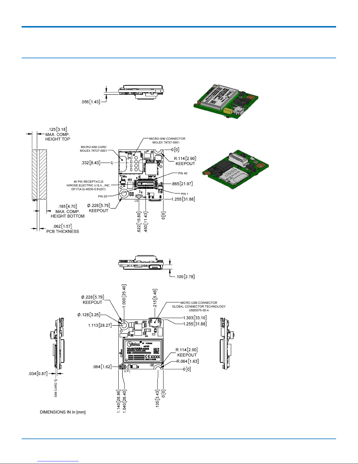
Chapter 2 – Mechanical Drawings
MTQN-MNG1-B01
6 MultiConnect®Dragonfly™Nano MTQN-MNG1-B01 Device Guide
Page 7
HARDWARE AND SPECIFICATIONS
Chapter 3 – Hardware and Specifications
Specifications
Category Description
Performance
1
3GPP Release 13 Cat M1 Half Duplex (Up to 375K bps downlink and uplink)
Frequency Band
(MHz)
AT&T Verizon
700 MHz (B12), 850 MHz (B5),
700 MHz (B13)
AWS1700 MHz (B4) and 1900 MHz
(B2)
Interface
Connectors 1 UFL (Cellular), 1x Micro USB, 1x 40-Pin Board-to-Board
Host Processor Cortex-M4 (STM32L471QG) 1 Mbyte Flash and 128 Kbyte SRAM (B01)
I/O 1 x UART, 1 x HS USB, 2 x SPI, 2 x I2C, up to 9 analog inputs and up to 29 digital input/output
SMS Mobile Terminate/Mobile Originate PDU / Text mode
Physical Description
Weight less than 0.3 oz (8.5g)
Dimensions 28.96mm x 32.51mm (1.14 x 1.28 inches). Refer to Mechanical Drawings for details.
Connectors
Antenna 1 surface mount U.FL: cellular
SIM Holder 1.8 V and 3 V Micro SIM (3FF) card. SIM denotes: Subscriber Identity Module.
Pin header 40-pin female for USB or UART
Environment
Operating
Temperature
Storage
2
-40° C to +85° C (-40° F to +185° F)
-40° C to +85° C (-40° F to +185° F)
Temperature
Humidity
1
Actual performance speeds may be affected by a variety of attributes such as cell tower distance, data loads,
3
15%-93% RH, non-condensing
packet sizes, etc.
2
Device has been tested up to +85° C. UL Recognized @ 85° C.
3
Radio performance may be affected by temperature extremes. This is normal.
The following table defines the remaining specifications for the MTQN-MNG1.
Category Description
Certifications and Compliance
MultiConnect®Dragonfly™Nano MTQN-MNG1-B01 Device Guide 7
Page 8
HARDWARE AND SPECIFICATIONS
Category Description
EMC Compliance FCC Part 15 Class B
Radio Compliance FCC Part 22, 24, 27
Safety Compliance UL/cUL 60950-1 2nd ED, IEC 60950-1 2nd ED +Am.2
Network PTCRB N/A
Carrier AT&T Verizon
40-Pin Connector Definitions
The Dragonfly™ Nano offers developers an FCC and carrier certified solution that makes connecting sensors and
other edge-of-network devices quick and easy.
40-Pin Connector
1 2 3 4 5 6 7 8 9 10 11 12 13 14 15 16 17 18 19 20
40 39 38 37 36 35 34 33 32 31 30 29 28 27 26 25 24 23 22 21
8 MultiConnect®Dragonfly™Nano MTQN-MNG1-B01 Device Guide
Page 9
HARDWARE AND SPECIFICATIONS
MTQN-MNG1-B01 Pin Definitions
Note:
To program and use the Dragonfly™ Nano, you will need a UDK2 Developer Kit.
For more pinout information and other details, refer to the STM32L471QG processor manual. In addition to their
stated functions, all GPIO pins (PA_*, PB_*, PC_*, PG_*) can also be used as Digital-In and Digital-Out interfaces.
Hardware Pinout Information
Processor Pin
Number
Processor Pin
Name
IO Type Net name 40 Pin UDK2 pin
/Arduino
Primary
Function
B5 PB6 FT_fa DBG_TX 1 Programming,
Output from
MTQN
A10 PA14_SWCLK FT J_TCK/SWCLK 2 Programming
A9 PA15 FT J_TDI/C_MON 3 Programming
A7 PB4 FT_a J_RST 4 Programming
J1 GND GND 5 GND
F2 VSS1 GND 13 GND
E3 VSS2 GND 28 GND
F6 VSS3 GND 36 GND
F12 VSS4 GND 37 GND
F11 VSS5 GND 5 GND
F7 VSS6 GND 5 GND
D3 VSS7 GND 5 GND
USB_DP USB_DP 6 USB_DP
USB_DM USB_DM 7 USB_DM
VCC-IN VCC-IN 8 VCC-IN
VCC-IN VCC-IN 33 VCC-IN
K3 PA2 FT_a IO_00/RXD 9 D1 Serial Comm
MultiConnect®Dragonfly™Nano MTQN-MNG1-B01 Device Guide 9
output from
MTQN
Page 10

HARDWARE AND SPECIFICATIONS
Processor Pin
Number
Processor Pin
Name
IO Type Net name 40 Pin UDK2 pin
/Arduino
Primary
Function
J5 PA7 FT_a IO_01/DCD 10 D4 Serial Comm
output from
MTQN
M5 PB0 TT_a IO_02/RI 11 D8 Serial Comm
output from
MTQN
M2 PA1 FT_a IO_03/RTS 12 D6 Serial Comm
input to MTQN
C5 PB5 FT_a IO_04/MOSI1 14 D11 GPIO / MOSI
output from
MTQN
G10 PG2 FT_s IO_05/SCK1 15 D13 GPIO & PA5 as
well
A3 PB8 FT_f IO_06/SCL/SS1 16 D15 GPIO, 4.7K pull
up
K10 PB15 FT IO_07/MOSI2 17 D2 GPIO / MOSI
output from
MTQN
J3 PC2 FT_a IO_08/MISO2 18 A0 GPIO / MISO
input to MTQN
D2 PE6 FT IO_09 19 A3 GPIO
C1 PC13 FT IO_10 20 A1 GPIO
L4 PA6 FT_a IO_11 21 A4 GPIO
K5 PC4 FT_a IO_12 22 A2 GPIO
L10 PB10 FT_f IO_13/SCK2 23 D9 GPIO
J6 PG8 FT_fs IO_14 24 A5 GPIO
B3 PB9 FT_f IO_15/SDA/SRDY25 D14 GPIO, 4.7K pull
up
F9 PG3 FT_s IO_16/MISO1 26 D12 GPIO / MISO
input to MTQN
E10 PC8 FT IO_17/SS2 27 D10 GPIO
L2 PA0 FT_a IO_18/CTS 29 D3 Serial Comm
output from
MTQN
D10 PA9 FT IO_19/DSR 30 D5 Serial Comm
output from
MTQN
10 MultiConnect®Dragonfly™Nano MTQN-MNG1-B01 Device Guide
Page 11

HARDWARE AND SPECIFICATIONS
Processor Pin
Number
Processor Pin
Name
IO Type Net name 40 Pin UDK2 pin
/Arduino
Primary
Function
H4 PG7 FT_fs IO_20/DTR 31 D7 Serial Comm
input to MTQN
L3 PA3 TT IO_21/TXD 32 D0 Serial Comm
input to MTQN
LS 34 Link status
output from
Cell radio, 47K
pull up
A8 PB3 FT_a J_TDO/SWO 38 JTAG
A11 PA13_SWDIO FT J_TMS/SWDIO 39 JTAG
B4 PB7 FT_fa DBG_RX 40 Programming,
Input to MTQN
A4 BOOT0 B 3V3 or GND Boot option,
tied low
GND
H2 NRST Reset N_RESET Reset Input,
47K pull up,
active low
NRST_IN 35 Reset input
from 40-Pin,
connected to
NRST by 47K
resistor
NRST_IN
L12 PB12 FT VCC-
IN_MEAS_EN
Control for
enabling
power
measurement,
pulled low
with 100K
resistor
H1 PC0 FT_fa VCC-IN_MEAS Ananlog power
measurement
B11 PC10 FT FLASH_SCK FLASH_SCK,
47K pull down
C10 PC11 FT FLASH_MISO FLASH_MISO
B10 PC12 FT FLASH_MOSI FLASH_MOSI
D1 PC14_OSC32IN FT 32K Clock 32K Clock
MultiConnect®Dragonfly™Nano MTQN-MNG1-B01 Device Guide 11
Page 12

HARDWARE AND SPECIFICATIONS
Processor Pin
Number
Processor Pin
Name
IO Type Net name 40 Pin UDK2 pin
/Arduino
Primary
Function
E1 PC15_OSC32OUTFT 32K Clock 32K Clock
K2 PC3 FT_a RADIO_PWR RADIO_PWR,
enable for cell
regulator, 47K
pull down
L5 PC5 FT_a 1V8_MON Radio Control
Feedback,
100K pull
down
E12 PC6 FT BUF_EN Buffer Power
Control, 100K
pull up, active
low
J12 PD10 FT RADIO_RI Serial for
Radio
J11 PD11 FT RADIO_CTS Serial for
Radio
J10 PD12 FT RADIO_RTS Serial for
Radio
H12 PD13 FT RADIO_DTR Serial for
Radio
H11 PD14 FT RADIO_DCD Serial for
Radio
H10 PD15 FT RADIO_DSR Serial for
Radio
K9 PD8 FT RADIO_TXD Serial for
Radio
K8 PD9 FT RADIO_RXD Serial for
Radio
A2 PE1 FT VMEM_EN Power control
for Flash, 100K
pull up, active
low
M9 PE11 FT CELL_GPIO5 GPIO to RADIO
M10 PE13 FT CELL_GPIO2 GPIO to RADIO
M11 PE14 FT CELL_GPIO3 GPIO to RADIO
M12 PE15 FT CELL_GPIO4 GPIO to RADIO
12 MultiConnect®Dragonfly™Nano MTQN-MNG1-B01 Device Guide
Page 13

HARDWARE AND SPECIFICATIONS
Processor Pin
Number
Processor Pin
Name
IO Type Net name 40 Pin UDK2 pin
/Arduino
Primary
Function
A1 PE3 FT VUSB_DET USB Select,
Active low for
Serial mode,
100K pull
down
B1 PE4 FT RADIO_ONOFF Radio power
control, 100K
pull down
E4 PF3 FT_a RADIO_RESET RADIO_RESET
control, 100K
pull down
D7 PG12 FT_s FLASH_NSS FLASH_NSS,
active low
E2 VBAT VRTC VRTC
G2 VDD1 3V3 3V3
H3 VDD2 3V3 3V3
G6 VDD3 3V3 3V3
G12 VDD4 3V3 3V3
C11 VDD5 3V3 3V3
G11 VDD6 3V3 3V3
C4 VDD7 3V3 3V3
M1 VDDA 3V3 3V3
G7 VDDIO2 3V3 3V3
L1 VREF+ 3V3 3V3
Data taken from STM32L471QG processor datasheet.
Key for IO type values:
FT 5V tolerant IO
TT 3.6V tolerant IO
B Dedicated Boot pin
RST Reset pin
_f IO, Fm+ capable
_a IO, with Analog supplied by VDDA
_s IO, supplied by VDDIO2
MultiConnect®Dragonfly™Nano MTQN-MNG1-B01 Device Guide 13
Page 14

HARDWARE AND SPECIFICATIONS
Software Pinout Information
The names in this table are defined in the PinNames.h file in mbed-os at the following path: mbedos\targets\target_stm\target_stm32l4\target_mts_dragonfly_l471qg
Pin UDK2 Primary Alternate names
PA_0 D3 UART2_CTS TIM5_1, ADC1_IN13,
ADC2_IN13, SERIAL_CTS,
IO_18, WAKEUP, LED1,
LED2, LED3, LED4
PA_1 D6 UART2_RTS TIM5_2, ADC1_IN6,
ADC2_IN6, SERIAL_RTS,
IO_03
PA_13 J_TMS
PA_14 J_TCK
PA_15 J_TDI TIM2_1
PA_2 D1 UART2_TX TIM2_3, TIM5_3,
ADC1_IN7, ADC2_IN7,
SERIAL_TX , IO_00
PA_3 D0 UART2_RX ADC1_IN8, ADC2_IN8,
SERIAL_RX , IO_21
PA_6 A4 IO_11 ADC1_IN11, ADC2_IN11
PA_7 D4 UART2_DCD TIM3_2, TIM7_1,
ADC1_IN12, ADC2_IN12,
SERIAL_DCD, IO_01
PA_9 D5 UART2_DSR SERIAL_DSR, IO_19
PB_0 D8 SERIAL_RI TIM3_3, ADC1_IN15,
ADC2_IN15, IO_02
PB_10 D9 SPI2_SCK IO_13
PB_12 VCC_IN_MEAS_EN
PB_15 D2 SPI2_MOSI IO_07
PB_3 J_TDO TIM2_2
PB_4 J_RST TIM3_1
PB_5 D11 SPI1_MOSI IO_04
PB_6 UART1_TX USBTX
PB_7 UART1_RX USBRX
PB_8 D15 I2C1_SCL TIM4_3, CAN1_RX, IO_06
PB_9 D14 I2C1_SDA CAN1_TX, IO_15
PC_0 VCC_IN_MEAS
PC_10 SPI3_SCK
14 MultiConnect®Dragonfly™Nano MTQN-MNG1-B01 Device Guide
Page 15

HARDWARE AND SPECIFICATIONS
Pin UDK2 Primary Alternate names
PC_11 SPI3_MISO
PC_12 SPI3_MOSI
PC_13 A1 IO_10
PC_14 32K
PC_15 32K
PC_2 A0 SPI2_MISO ADC1_IN3, ADC2_IN3,
ADC3_IN3, IO_08,
ADC1_IN1, ADC2_IN1,
ADC3_IN1
PC_3 RADIO_PWR
PC_4 A2 IO_12 ADC1_IN13, ADC2_IN13
PC_5 MON_1V8
PC_6 BUF_EN
PC_8 D10 IO_17 TIM8_3
PD_10 RADIO_RI MDMRI
PD_11 RADIO_CTS MDMCTS, UART3_CTS
PD_12 RADIO_RTS MDMRTS, UART3_RTS
PD_13 RADIO_DTR MDMDTR
PD_14 RADIO_DCD MDMDCD
PD_15 RADIO_DSR MDMDSR
PD_8 RADIO_TX MDMTXD
PD_9 RADIO_RX MDMRXD , UART3_RX
PE_1 VMEM_EN
PE_11 CELL_GPIO5
PE_13 CELL_GPIO2
PE_14 CELL_GPIO3
PE_15 CELL_GPIO4
PE_3 VUSB_DET
PE_4 RADIO_ONOFF MDMPWRON
PE_6 A3 IO_09
PF_3 RADIO_RESET MDMRST
PG_12 SPI3_SSEL
PG_2 D13 SPI1_SCK IO_05
PG_3 D12 SPI1_MISO IO_16
MultiConnect®Dragonfly™Nano MTQN-MNG1-B01 Device Guide 15
Page 16

HARDWARE AND SPECIFICATIONS
Pin UDK2 Primary Alternate names
PG_7 D7 UART2_DTR I2C3_SCL, SERIAL_DTR,
IO_20
PG_8 A5 IO_14 I2C3_SDA
Communications Flow
MTQN-MNG1-B01
The MTQN-MNG1-B01 provides full UART from the cellular radio to the processor as well as the user application.
Model B01 provides a direct USB interface connection to the radio, but not through the 40-pin connector.
Switching between the USB interface and serial port requires a reset. The cellular radio checks for a USB
connection upon reset. If USB is not present, it only uses the serial port. If USB is present upon reset, it only uses
USB.
Electrical Characteristics
Operating Conditions
Parameter Minimum Volts Maximum Volts
Supply Range - Vcc 3.2 5.25
Absolute Maximum Ratings
Symbol Description Conditions Min. Max. Unit
SIM SIM interface Input DC voltage at SIM digital
interfaces pins
P_ANT Antenna power Input RF power at ANT pin -22 dbM
Rho_ANT Antenna ruggedness Output RF load mismatch
ruggedness at ANT pins
-0.3 3.9 V
10.1 VSWR
16 MultiConnect®Dragonfly™Nano MTQN-MNG1-B01 Device Guide
Page 17

HARDWARE AND SPECIFICATIONS
Symbol Description Conditions Min. Max. Unit
tstg Storage Temperature -40 85 °C
V
P
V
- V
DDX
SS
2
V
IN
Voltage at any pin Voltage at any signal pin -0.3 4 V
External voltage V
DDX
, V
DDA,VDDIO2
, V
BAT
1
-0.3 4 V
Input Voltage Input voltage on FT_xxx pins VSS-0.3 min (VDD,
V
DDA,VDDIO2
4.0
)+
3 & 4
V
Input voltage on TT_xx pins VSS-0.3 4.0 V
Input voltage on BOOT0 pin V
SS
9.0 V
Input voltage on any other pins VSS-0.3 4.0 V
|ΔV
DDx|
Variations between
power pins
Variations between
different V
power pins of
DDX
N/A 50 mV
the same domain
|V
| Variations between
SSx-VSS
ground pins
Variations between all the
different ground pins
5
N/A 50 mV
Data taken from STM32L471QG processor datasheet.
(1) All main power (VDD, V
DDA
, V
DDIO2
, V
) and ground (VSS, V
BAT
) pins must always be connected to the external power
SSA
(2) VINmaximum must always be respected. Refer to Nominal Ratings for the maximum allowed injected current
values.
(3) This formula has to be applied only on the power supplies related to the IO structure described in the pin
definition table.
(4) To sustain a voltage higher than 4 V the internal pull-up/pull-down resistors must be disabled.
(5) Include VREF- pin.
Nominal Ratings
Symbol Ratings Max Voltage
(mA)
ΣIV
ΣIV
IV
IV
DD
SS
DD(PIN)
SS(PIN)
Total current into sum of all VDD power lines (source)
Total current out of sum of all VSS ground lines (sink)
Maximum current into each VDD power pin (source)
Maximum current out of each VSS ground pin (sink)
1
1
1
1
150
150
100
100
MultiConnect®Dragonfly™Nano MTQN-MNG1-B01 Device Guide 17
Page 18

HARDWARE AND SPECIFICATIONS
Symbol Ratings Max Voltage
(mA)
I
IO(PIN)
Output current sunk by any I/O and control pin except FT_f 20
Output current sunk by any FT_f pin 20
Output current sourced by any I/O and control pin 20
ΣI
IO(PIN)
I
INJ(PIN)
3
Total output current sunk by sum of all I/Os and control
pins
2
Total output current sourced by sum of all I/Os and control
pins
2
Injected current on FT_xxx, TT_xx, RST and B pins, except
PA4, PA5
100
100
-5/+0
4
Injected current on PA4, PA5
Σ|I
| Total injected current (sum of all I/Os and control pins)
INJ(PIN)
5
-5/0
25
Data taken from STM32L471QG processor datasheet.
(1) All main power (VDD, V
DDA
, V
DDIO2
, V
) and ground (VSS, V
BAT
) pins must always be connected to the external
SSA
power, in permitted range.
(2) This current consumption must be correctly distributed over all I/Os and control pins. The total output current
must not be sunk/sourced between two consecutive power supply pins referring to high pin count QFP packages.
(3) Positive injection (when VIN> V
) is not possible on these I/Os and does not occur for input voltages lower
DDIOx
than the specified maximum value.
(4) A negative injection is induced by VIN< V
SS. IINJ(PIN)
must never be exceeded. Refer to the Absolute Maximum
Ratings table for the minimum allowed input voltage values.
(5) When several inputs are submitted to a current injection, the maximum Σ|I
| is the absolute sum of the
INJ(PIN)
negative injected currents (instantaneous values).
Power Draw
Voltage Radio
Protocol
3.8 VDC LTE 21.943 μA
5.0 VDC LTE 4.702 μA 155.421 mA 315.532 mA 0.00792
1
Maximum Power: The continuous current during maximum data rate with the radio transmitter at maximum
power.
2
Tx Pulse: The average peak current during a GSM 850 transmission burst period or LTE connection. The
transmission burst duration for GSM 850 can vary, depending on what transmission scheme is being deployed
(GPRS Class 8, Class 10, GSM, etc.).
Sleep Mode
Current
Power Saving
Mode
(AVG)
Measured
Current at
Max Power
TX Pulse2(AVG)
Amplitude Current for
Peak Current
1
Total Inrush
Charge3in
MilliCoulombs
(mC)
18 MultiConnect®Dragonfly™Nano MTQN-MNG1-B01 Device Guide
Page 19

3
Inrush Charge: The total inrush charge at power on.
USB Cable Recommendations
If your device has a USB connector, to avoid enumeration or power issues:
Use a high-speed USB cable that is as short as possible.
Use a well-shielded cable with at least 24 AWG wire pair for power/ground and 28 AWG wire pair for data
lines.
If possible, use a USB port that connects directly to the motherboard rather than a USB port with added
cabling inside the computer chassis.
Use USB 3.0 ports if available. These ports are typically rated for more current.
You can order the USB cable through MultiTech. The part number is: CA-USB-A-MICRO-B-3.
Device Reset
MTQN-MNG1-B01
There are two components to reset.
HARDWARE AND SPECIFICATIONS
1. Processor reset: Several reset methods are available and all are documented in the STM32L471QG
reference guide.
2. Radio reset: The processor controls the RESET_N and PWR_ON pins to the radio. The functionality of
those pins is described in the ublox SARA_R4 data sheet.
Note:
N_RESET of the 40 pin connector is directly connected to NRST of the STM32L471QG processor. The
processor controls the PWR_ON(RADIO_ONOFF/PE_4) and RESET_N(RADIO_RESET/PF_3) pins to the radio.
Powering Down the Cellular Radio
CAUTION:: Failing to properly power down the cellular radio before removing power may corrupt the radio's file
system.
To properly power down the cellular radio, use one of the following methods:
1. Issue command AT+CPWROFF then either wait 40s or until 1.8v from the cellular radio goes low.
Processor pin PC5 (Mbed pin name MON_1V8) has 1.8v from the radio connected to it.
2. Hold pin processor PE_4 (Mbed pin name RADIO_ONOFF or MDMPWRON) low for at least 1.5s. 1.8v
from the radio should go low.
3. If neither of the above two options are successful, an emergency power down can be performed by
holding processor pin PF_3 (mbed pin name RADIO_RESET) low for 10s. As always, power down is
confirmed by monitoring 1.8v from the radio.
Low Power Modes
To achieve lowest power consumption, we recommend powering down the radio then configuring RADIO_PWR,
VMEM_EN and BUF_EN as analog inputs with no pull resistor. The last step is to place the processor in a low power
mode of your choosing.
MultiConnect®Dragonfly™Nano MTQN-MNG1-B01 Device Guide 19
Page 20

HARDWARE AND SPECIFICATIONS
WARNING:If your application is using the on board flash memory part, make sure any flash accesses are complete
before removing power or the memory may be corrupted.
Cellular Radio Low Power
Note: Refer to the U-blox AT command guide for details on AT commands.
1. Powering Down - See Powering Down The Cellular Radio section
2. PSM mode- AT+CPSMS command
3. eDRX- AT+CEDRXS command
4. Device functionality- AT+CEDRXS command
Power to Cellular Radio
After power down, RADIO_PWR can be configured as an analog input with no pull resistor to disable the power
supply regulator that powers the radio. There is an on board resistor that sets the RADIO_PWR signal level so that
the regulator is disabled.
On Board Flash Memory
After power down, RADIO_PWR can be configured as an analog input with no pull resistor to disable the power
supply regulator that powers the radio. There is an on board resistor that sets the RADIO_PWR signal level so that
the regulator is disabled.
Level translator
BUF_EN can be configured as an analog input with no pull resistor to disable the level shifter. There is an on board
resistor that sets the BUF_EN signal level so power is removed.
STM32L471QG processor
See the STM32L471QG data sheet for low power modes.
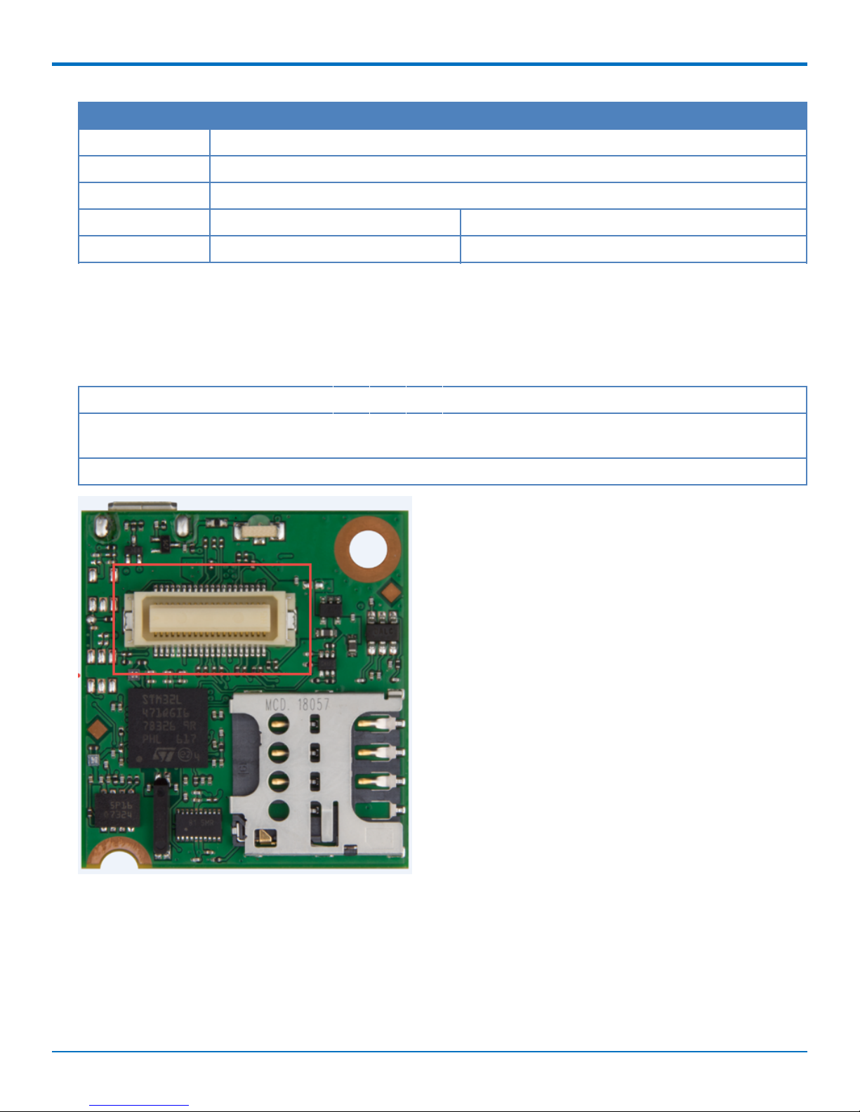
Installing a SIM Card
Note: All Dragonfly™ Nano models require the use of a Micro SIM (3FF) card.
To install the SIM card:
Refer to the image below.
Slide the SIM card completely into the SIM holder.
20 MultiConnect®Dragonfly™Nano MTQN-MNG1-B01 Device Guide
Page 21

Configuring u-blox Cellular Radio
HARDWARE AND SPECIFICATIONS
This MNG1 device uses a cellular radio that can operate on different carrier networks (not simultaneously).
Your device is configured in the factory for Cat M1 mode and to automatically detect your SIM to register on your
carrier network provided their network is on supported list of MNOs for the u-blox cellular radio. Typically, most
customers should not need to use the commands in this section.
If your carrier network is not on the supported list of MNOs, you must set to Cat M1 mode and follow the
instructions per that scenario below.
The MNG1 model is licensed to operate on both Verizon or AT&T networks. Refer to the Sara-R4/N4 series AT
Commands Manual for more details.
Note: If your device is on +UMNOPROF: 0 (SW default), there is no network and you must set one.
Set at the factory (factory default on MNG1):
1. This command sets your device in Cat M1 mode:
AT+URAT=7
2. This command automatically detects the carrier network based on your device SIM, provided that
your carrier network (or MNO) is on the supported list:
AT+UMNOPROF=1
To set or switch carrier networks:
1. Deregister the module from the network or perform an AT+CFUN=0 cycle:
AT+CFUN=0
2. Set the carrier network (refer to the list of +UMNOPROF values):
To AT&T:
AT+UMNOPROF=2
MultiConnect®Dragonfly™Nano MTQN-MNG1-B01 Device Guide 21
Page 22

HARDWARE AND SPECIFICATIONS
To Verizon:
AT+UMNOPROF=3
3. Reboot the module in order to apply the new configuration:
AT+CFUN=15
If the APN is known and will not change: We recommend hard-coding the MNO and setting the PDP context
manually. The following example of an AT command sequence is for AT&T.
AT+CFUN=0
AT+UMNOPROF=2
AT+CGDCONT=1, "IPV4V6", "phone"
AT+CFUN=15
If the MNO is not listed: the following command sequence is recommended.
NOTE: We recommend changing +UMNOPROF separately before +UBANDMASK.
AT+CFUN=0
AT+UMNOPROF=0
AT+CFUN=15
AT+CFUN=0
AT+CGDCONT=..
AT+UBANDMASK=..
AT+CFUN=15
To configure the supported radio bands: Use the +UBANDMASK command if your MNO is not listed by the
+UMNOPROF command. Refer to your specific carrier regarding available bands.
USB Driver Installation
For the Windows USB driver, refer to the SARA-R4 USB Driver Installation Guide on the product page of the
Multitech website. The driver is located under the Downloads section of the product page.
For the Linux USB driver, if your Linux OS does not automatically detect your device, you may need to execute a
script. This script adds the MTQN vendor ID and product ID to the USB serial driver. Download the zip file which
contains this script and readme file under Downloads on the product page of the website.
22 MultiConnect®Dragonfly™Nano MTQN-MNG1-B01 Device Guide
Page 23

Chapter 4 – Antennas
Antenna
Devices were approved with the following antenna or for alternate antennas meeting the given specifications:
Manufacturer: Wieson
Description: LTE Antenna with SMA-Male Connector
Model Number GY115IE002-001
MultiTech ordering information:
Model Quantity
ANLTE4-1HRA 1
ANLTE4-2HRA 2
ANLTE4-10HRA 10
ANTENNAS
ANLTE4-50HRA 50
Antenna Specifications
Category Description
Frequency Range 0.698 - 0.96 GHz
1710 - 2170 GHz
2.30 - 2.69 GHz
VSWR 3:1 maximum
Gain 2.06 dBi
Impedance 50Ω nominal
Radiation Omni-directional
Polarization Linear, vertical
MultiConnect®Dragonfly™Nano MTQN-MNG1-B01 Device Guide 23
Page 24

SAFETY INFORMATION
Chapter 5 – Safety Information
Handling Precautions
To avoid damage due to the accumulation of static charge, use proper precautions when handling any cellular
device. Although input protection circuitry has been incorporated into the devices to minimize the effect of static
build-up, use proper precautions to avoid exposure to electronic discharge during handling and mounting the
device.
Radio Frequency (RF) Safety
Due to the possibility of radio frequency (RF) interference, it is important that you follow any special regulations
regarding the use of radio equipment. Follow the safety advice given below.
Operating your device close to other electronic equipment may cause interference if the equipment is
inadequately protected. Observe any warning signs and manufacturers’ recommendations.
Different industries and businesses restrict the use of cellular devices. Respect restrictions on the use of
radio equipment in fuel depots, chemical plants, or where blasting operations are in process. Follow
restrictions for any environment where you operate the device.
Do not place the antenna outdoors.
Switch OFF your wireless device when in an aircraft. Using portable electronic devices in an aircraft may
endanger aircraft operation, disrupt the cellular network, and is illegal. Failing to observe this restriction
may lead to suspension or denial of cellular services to the offender, legal action, or both.
Switch OFF your wireless device when around gasoline or diesel-fuel pumps and before filling your vehicle
with fuel.
Switch OFF your wireless device in hospitals and any other place where medical equipment may be in use.
Sécurité relative aux appareils à radiofréquence (RF)
À cause du risque d'interférences de radiofréquence (RF), il est important de respecter toutes les réglementations
spéciales relatives aux équipements radio. Suivez les conseils de sécurité ci-dessous.
Utiliser l'appareil à proximité d'autres équipements électroniques peut causer des interférences si les
équipements ne sont pas bien protégés. Respectez tous les panneaux d'avertissement et les
recommandations du fabricant.
Certains secteurs industriels et certaines entreprises limitent l'utilisation des appareils cellulaires. Respectez
ces restrictions relatives aux équipements radio dans les dépôts de carburant, dans les usines de produits
chimiques, ou dans les zones où des dynamitages sont en cours. Suivez les restrictions relatives à chaque
type d'environnement où vous utiliserez l'appareil.
Ne placez pas l'antenne en extérieur.
Éteignez votre appareil sans fil dans les avions. L'utilisation d'appareils électroniques portables en avion est
illégale: elle peut fortement perturber le fonctionnement de l'appareil et désactiver le réseau cellulaire. S'il
ne respecte pas cette consigne, le responsable peut voir son accès aux services cellulaires suspendu ou
interdit, peut être poursuivi en justice, ou les deux.
Éteignez votre appareil sans fil à proximité des pompes à essence ou de diesel avant de remplir le réservoir
de votre véhicule de carburant.
Éteignez votre appareil sans fil dans les hôpitaux ou dans toutes les zones où des appareils médicaux sont
susceptibles d'être utilisés.
24 MultiConnect®Dragonfly™Nano MTQN-MNG1-B01 Device Guide
Page 25

SAFETY INFORMATION
General Safety
The device is designed for and intended to be used in fixed and mobile applications. Fixed means the device is
physically secured at one location and cannot be easily moved to another location. Mobile means the device is
used in other than fixed locations.
CAUTION:Maintain a separation distance of at least 20 cm (8 inches) between the transmitter’s antenna and the
body of the user or nearby persons. The device is not designed for or intended to be used in portable applications
within 20 cm (8 inches) of the user’s body.
Attention:Maintenir une distance d'au moins 20 cm (8 po) entre l'antenne du récepteur et le corps de l'utilisateur
ou à proximité de personnes. Le modem n'est pas conçu pour, ou destinés à être utilisés dans les applications
portables, moins de 20 cm du corps de l'utilisateur.
Interference with Pacemakers and Other Medical Devices
Potential Interference
Radio frequency energy (RF) from cellular devices can interact with some electronic devices. This is
electromagnetic interference (EMI). The FDA helped develop a detailed test method to measure EMI of implanted
cardiac pacemakers and defibrillators from cellular devices. This test method is part of the Association for the
Advancement of Medical Instrumentation (AAMI) standard. This standard allows manufacturers to ensure that
cardiac pacemakers and defibrillators are safe from cellular device EMI.
The FDA continues to monitor cellular devices for interactions with other medical devices. If harmful interference
occurs, the FDA will assess the interference and work to resolve the problem.
Precautions for pacemaker wearers
If EMI occurs, it could affect a pacemaker in one of three ways:
Stop the pacemaker from delivering the stimulating pulses that regulate the heart's rhythm.
Cause the pacemaker to deliver the pulses irregularly.
Cause the pacemaker to ignore the heart's own rhythm and deliver pulses at a fixed rate.
Based on current research, cellular devices do not pose a significant health problem for most pacemaker wearers.
However, people with pacemakers may want to take simple precautions to be sure that their device doesn't cause
a problem.
Keep the device on the opposite side of the body from the pacemaker to add extra distance between the
pacemaker and the device.
Avoid placing a turned-on device next to the pacemaker (for example, don’t carry the device in a shirt or
jacket pocket directly over the pacemaker).
Vehicle Safety
When using your device in a vehicle:
Do not use this device while driving.
Respect national regulations on the use of cellular devices in vehicles.
If incorrectly installed in a vehicle, operating the wireless device could interfere with the vehicle’s
electronics. To avoid such problems, use qualified personnel to install the device. The installer should verify
the vehicle electronics are protected from interference.
Using an alert device to operate a vehicle’s lights or horn is not permitted on public roads.
MultiConnect®Dragonfly™Nano MTQN-MNG1-B01 Device Guide 25
Page 26

SAFETY INFORMATION
UL evaluated this device for use in ordinary locations only. UL did NOT evaluate this device for installation in
a vehicle or other outdoor locations. UL Certification does not apply or extend to use in vehicles or outdoor
applications.
Device Maintenance
When maintaining your device:
Do not attempt to disassemble the device. There are no user serviceable parts inside.
Do not misuse the device. Follow instructions on proper operation and only use as intended. Misuse could
make the device inoperable, damage the device and/or other equipment, or harm users.
Do not apply excessive pressure or place unnecessary weight on the device. This could result in damage to
the device or harm to users.
Do not use this device in explosive or hazardous environments unless the model is specifically approved for
such use. The device may cause sparks. Sparks in explosive areas could cause explosion or fire and may
result in property damage, severe injury, and/or death.
Do not expose your device to any extreme environment where the temperature or humidity is high. Such
exposure could result in damage to the device or fire.
Do not expose the device to water, rain, or spilled beverages. It is not waterproof. Exposure to liquids could
result in damage to the device.
Do not place the device alongside computer discs, credit or travel cards, or other magnetic media. The
information contained on discs or cards may be affected by the device.
Using accessories, such as antennas, that MultiTech has not authorized or that are not compliant with
MultiTech's accessory specifications may invalidate the warranty.
If the device is not working properly, contact MultiTech Technical Support.
User Responsibility
Respect all local regulations for operating your wireless device. Use the security features to block unauthorized use
and theft.
26 MultiConnect®Dragonfly™Nano MTQN-MNG1-B01 Device Guide
Page 27

GETTING STARTED
Chapter 6 – Getting Started
Developing with an MTQN in Mbed
The MTQN ships with AT pass-through firmware, which directly connects the cellular radio to a serial port made
available via micro USB connector J6 on the MTUDK2-ST-CELL developer board. The firmware:
Runs at 115200 baud by default to match with the cellular radio’s default baud rate.
Prints debug messages from the debug port at 115200 baud.
Allows users to increase or decrease the application’ s baud rate by entering a plus (+) or minus (-) character
on the USB debug port. Issuing a plus or minus character on the USB debug port changes the external serial
port speed as well as the speed of the link between the processor and the radio. The speed of the USB
debug port on reset is always 115200 to match the radio’s default regardless of the baud rate used at the
time of reset.
Uses RTS/CTS flow control on the serial connection to the radio and on the external serial connection.
Enables RTS/CTS flow control on terminal emulators used with the AT pass-through firmware.
Mbed Documentation
ARM Mbed is a free, open-source platform and operating system for embedded devices using the ARM Cortex-M
microcontrollers. The Mbed website provides free software libraries, hardware designs, and online tools for rapid
prototyping of products. The platform includes a standards-based C/C++ SDK, a microcontroller HDK, and
supported development boards, an online compiler and online developer collaboration tools.
Programming the MTQN Microcontroller
With the MTQN and the MTUDK2-ST-CELL developer board, use the ARM Mbed ecosystem to program the
microcontroller. Compile in the cloud or locally, copy the resulting binary file to the Mbed USB drive, and reset the
MTQN-MNG1.
MTQN software is open source.
Useful Links
Description Link
MTQN Mbed page: https://os.mbed.com/platforms/MTS-Dragonfly-Nano/
Explore Mbed: https://os.mbed.com/explore/
MTUDK2-ST-CELL developer
guides (see Manuals for
different versions)
Documentation on Mbed: https://os.mbed.com/docs/latest
Serial Flash Datasheet (pdf): http://www.micron.com (refer to P/N M25P16)
https://www.multitech.com/models/94557065LF
Additional Information: https://www.multitech.com/brands/multiconnect-dragonfly-nano
Based on current research, cellular devices do not pose a significant health problem for most pacemaker wearers.
However, people with pacemakers may want to take simple precautions to be sure that their device doesn't cause
a problem.
MultiConnect®Dragonfly™Nano MTQN-MNG1-B01 Device Guide 27
Page 28

GETTING STARTED
Keep the device on the opposite side of the body from the pacemaker to add extra distance between the
pacemaker and the device.
Avoid placing a turned-on device next to the pacemaker (for example, don’t carry the device in a shirt or
jacket pocket directly over the pacemaker).
ST Microcontroller STM32L471QG
For the ST microcontroller STM32L471QG reference manual and datasheet, refer to the product page at
https://www.st.com/en/microcontrollers/stm32l471qg.html.
28 MultiConnect®Dragonfly™Nano MTQN-MNG1-B01 Device Guide
Page 29

Chapter 7 – Labels
Approvals and Certifications
This device is an industry and/or carrier approved modem. In most cases, when integrated and used with an
antenna system that was part of the MultiTech modem certification, additional approvals or certifications are not
required for the device that you develop as long as the following requirements are met:
PTCRB Requirements: The antenna system cannot be altered.
Model Identification: The MultiTech model identification allows the carrier to verify the modem as one of
its approved models. This information is located on the modem's label below the bar code.
Example Labels
The label shown is not the actual size.
This device complies with part 15 of the FCC Rules. Operation is subject to the following two conditions: (1) This
device may not cause harmful interference, and (2) this device must accept any interference received, including
interference that may cause undesired operation.
LABELS
Note: Actual labels vary depending on the regulatory approval markings and content.
This device complies with part 15 of the FCC Rules. Operation is subject to the following two conditions: (1) This
device may not cause harmful interference, and (2) this device must accept any interference received, including
interference that may cause undesired operation.
The label shown is not the actual size.
1 - MultiTech Model Identification
2 - MultiTech Ordering Part Number
3 - IMEI
Device Label Package Label
MultiConnect®Dragonfly™Nano MTQN-MNG1-B01 Device Guide 29
Page 30

REGULATORY INFORMATION
Chapter 8 – Regulatory Information
47 CFR Part 15 Regulation Class B Devices
This equipment has been tested and found to comply with the limits for a Class B digital device, pursuant to part
15 of the FCC Rules. These limits are designed to provide reasonable protection against harmful interference in a
residential installation. This equipment generates, uses, and can radiate radio frequency energy and, if not installed
and used in accordance with the instructions, may cause harmful interference to radio communications. However,
there is no guarantee that interference will not occur in a particular installation. If this equipment does cause
harmful interference to radio or television reception, which can be determined by turning the equipment off and
on, the user is encouraged to try to correct the interference by one or more of the following measures:
Reorient or relocate the receiving antenna.
Increase the separation between the equipment and receiver.
Connect the equipment into an outlet on a circuit different from that to which the receiver is connected.
Consult the dealer or an experienced radio/TV technician for help.
Warning: Changes or modifications to this unit not expressly approved by the party responsible for compliance
could void the user’s authority to operate the equipment.
FCC Interference Notice
This device complies with part 15 of the FCC Rules. Operation is subject to the following two conditions: (1) This
device may not cause harmful interference, and (2) this device must accept any interference received, including
interference that may cause undesired operation.
FCC Grant
FCC Grant Part 22, 24, and 27
The u-blox AG: SARA-R4 cellular module has been issued an equipment authorization by the FCC.
Category Description
FCC Identifier XPY2AGQN4NNN (for SARA-R410M-02B)
Equipment Class PCS Licensed Transmitter
Notes Cellular Module
FCC Rule Parts 22H, 24E, 27
Approval Single Modular
Component Description
SARA-R410M-02B LTE module for North America (AT&T/Verizon); Cat M1
The device operates within approved frequencies overlapping with the following cellular bands:
LTE 2, 1900 PCS UP
LTE 25, 1900+ UP
LTE 35, TD PCS Lower DOWN
30 MultiConnect®Dragonfly™Nano MTQN-MNG1-B01 Device Guide
Page 31

UMTS CH 2 UP
UMTS CH 25 UP
UMTS CH 35 DOWN
The following table provides the certified radio frequency data for this device:
REGULATORY INFORMATION
FCC Rule
Parts
Frequency Range Output Watts (mW) Frequency Tolerance Emission
Designator
27 699 - 716 MHz 0.316 1.0 PM 1M11G7D
27 699 - 716 MHz 0.316 1.0 PM 1M11W7D
22H 824 - 849 MHz 0.316 1.0 PM 1M11G7D
22H 824 - 849 MHz 0.316 1.0 PM 1M11W7D
27 1.71 - 1.755 GHz 0.316 1.0 PM 1M24G7D
27 1.71 - 1.755 GHz 0.316 1.0 PM 1M13W7D
24E 1.85 - 1.91 GHz 0.316 1.0 PM 1M12G7D
24E 1.85 - 1.91 GHz 0.316 1.0 PM 1M12W7D
Single Modular Approval. Power output listed is conducted. This device is approved for mobile and fixed use with
respect to RF exposure compliance, and may only be marketed to OEM installers. The antenna(s) used for this
transmitter, as described in this filing, must be installed to provide a separation distance of at least 20 cm from all
persons. Installers and end-users must be provided with operating conditions for satisfying RF exposure
compliance.
Maximum permitted antenna gain/cable:
3.67 dbi for 700 MHz
4.10 dBi for 850 MHz
6.74 dBi for 1700 MHz
7.12 dBi for 1900 MHz
The final product operating with this transmitter must include operating instructions and antenna installation
instructions, for end-users and installers to satisfy RF exposure compliance requirements. Compliance of this device
in all final product configurations is the responsibility of the Grantee. Installation of this device into specific final
products may require the submission of a Class II permissive change application containing data pertinent to RF
Exposure, spurious emissions, ERP/EIRP, and host/module authentication, or new application if appropriate.
This device contains GSM functions that are not operational in the U.S. Territories. This filing is only applicable for
U.S. operations.
MultiConnect®Dragonfly™Nano MTQN-MNG1-B01 Device Guide 31
Page 32

ENVIRONMENTAL NOTICES
Chapter 9 – Environmental Notices
Waste Electrical and Electronic Equipment Statement
Note: This statement may be used in documentation for your final product applications.
WEEE Directive
The WEEE Directive places an obligation on EU-based manufacturers, distributors, retailers, and importers to takeback electronics products at the end of their useful life. A sister directive, ROHS (Restriction of Hazardous
Substances) complements the WEEE Directive by banning the presence of specific hazardous substances in the
products at the design phase. The WEEE Directive covers all MultiTech products imported into the EU as of August
13, 2005. EU-based manufacturers, distributors, retailers and importers are obliged to finance the costs of recovery
from municipal collection points, reuse, and recycling of specified percentages per the WEEE requirements.
Instructions for Disposal of WEEE by Users in the European Union
The symbol shown below is on the product or on its packaging, which indicates that this product must not be
disposed of with other waste. Instead, it is the user's responsibility to dispose of their waste equipment by handing
it over to a designated collection point for the recycling of waste electrical and electronic equipment. The separate
collection and recycling of your waste equipment at the time of disposal will help to conserve natural resources
and ensure that it is recycled in a manner that protects human health and the environment. For more information
about where you can drop off your waste equipment for recycling, please contact your local city office, your
household waste disposal service or where you purchased the product.
July, 2005
Restriction of the Use of Hazardous Substances (RoHS)
Multi-Tech Systems, Inc.
Certificate of Compliance
2011/65/EU
Multi-Tech Systems, Inc. confirms that its embedded products comply with the chemical concentration limitations
set forth in the directive 2011/65/EU of the European Parliament (Restriction of the use of certain Hazardous
Substances in electrical and electronic equipment - RoHS).
These MultiTech products do not contain the following banned chemicals1:
Lead, [Pb] < 1000 PPM
Mercury, [Hg] < 1000 PPM
32 MultiConnect®Dragonfly™Nano MTQN-MNG1-B01 Device Guide
Page 33

ENVIRONMENTAL NOTICES
Hexavalent Chromium, [Cr+6] < 1000 PPM
Cadmium, [Cd] < 100 PPM
Polybrominated Biphenyl, [PBB] < 1000 PPM
Polybrominated Diphenyl Ether, [PBDE] < 1000 PPM
Environmental considerations:
Moisture Sensitivity Level (MSL) =1
Maximum Soldering temperature = 260C (in SMT reflow oven)
1
Lead usage in some components is exempted by the following RoHS annex, therefore higher lead concentration
would be found in some modules (>1000 PPM);
- Resistors containing lead in a glass or ceramic matrix compound.
REACH Statement
Registration of Substances
After careful review of the legislation and specifically the definition of an “article” as defined in EC Regulation
1907/2006, Title II, Chapter 1, Article 7.1(a)(b), it is our current view that Multi-Tech Systems, Inc. products would
be considered as “articles.” In light of the definition in § 7.1(b) which requires registration of an article only if it
contains a regulated substance that “is intended to be released under normal or reasonably foreseeable conditions
of use,” our analysis is that Multi-Tech Systems, Inc. products constitute nonregisterable articles for their intended
and anticipated use.
Substances of Very High Concern (SVHC)
Per the candidate list of Substances of Very High Concern (SVHC) published October 28, 2008 we have reviewed
these substances and certify the Multi-Tech Systems, Inc. products are compliant per the EU “REACH”
requirements of less than 0.1% (w/w) for each substance. If new SVHC candidates are published by the European
Chemicals Agency, and relevant substances have been confirmed to be greater than 0.1% (w/w), Multi-Tech
Systems, Inc. will provide updated compliance status.
Multi-Tech Systems, Inc. also declares it has been duly diligent in ensuring that the products supplied are compliant
through a formalized process which includes collection and validation of materials declarations and selective
materials analysis where appropriate. This data is controlled as part of a formal quality system and will be made
available upon request.
MultiConnect®Dragonfly™Nano MTQN-MNG1-B01 Device Guide 33
Page 34

ENVIRONMENTAL NOTICES
Information on HS/TS Substances According to Chinese Standards (in
Chinese)
依依照照中中国国标标准准的的有有毒毒有有害害物物质质信信息息
根据中华人民共和国信息产业部 (MII) 制定的电子信息产品 (EIP) 标准-中华人民共和国《电子信息产品污染
控制管理办法》(第 39 号),也称作中国 RoHS, 下表列出了 Multi-Tech Systems, Inc. 产品中可能含有的有毒
物质 (TS) 或有害物质 (HS) 的名称及含量水平方面的信息。
有有害害//有有毒毒物物质质//元元素素
成成分分名名称称
印刷电路板
电阻器
电容器
铁氧体磁环
继电器/光学部件
ICs O O O O O O
二极管/晶体管
振荡器和晶振
调节器
电压传感器
变压器
扬声器
连接器
LEDs O O O O O O
铅铅 (PB) 汞汞 (Hg) 镉镉 (CD) 六六价价铬铬 (CR6+)
O O O O O O
X O O O O O
X O O O O O
O O O O O O
O O O O O O
O O O O O O
X O O O O O
O O O O O O
O O O O O O
O O O O O O
O O O O O O
O O O O O O
多多溴溴联联苯苯
(PBB)
多多溴溴二二苯苯醚醚
(PBDE)
螺丝、螺母以及其它五金件
交流-直流电源
软件/文档 CD
手册和纸页
底盘
X 表示所有使用类似材料的设备中有害/有毒物质的含量水平高于 SJ/Txxx-2006 限量要求。
O 表示不含该物质或者该物质的含量水平在上述限量要求之内。
34 MultiConnect®Dragonfly™Nano MTQN-MNG1-B01 Device Guide
X O O O O O
O O O O O O
O O O O O O
O O O O O O
O O O O O O
Page 35

ENVIRONMENTAL NOTICES
Information on HS/TS Substances According to Chinese Standards
In accordance with China's Administrative Measures on the Control of Pollution Caused by Electronic Information
Products (EIP) # 39, also known as China RoHS, the following information is provided regarding the names and
concentration levels of Toxic Substances (TS) or Hazardous Substances (HS) which may be contained in Multi-Tech
Systems Inc. products relative to the EIP standards set by China's Ministry of Information Industry (MII).
Hazardous/Toxic Substance/Elements
Name of the Component Lead
(PB)
Printed Circuit Boards O O O O O O
Resistors X O O O O O
Capacitors X O O O O O
Ferrite Beads O O O O O O
Relays/Opticals O O O O O O
ICs O O O O O O
Diodes/ Transistors O O O O O O
Oscillators and Crystals X O O O O O
Regulator O O O O O O
Voltage Sensor O O O O O O
Transformer O O O O O O
Speaker O O O O O O
Connectors O O O O O O
Mercury
(Hg)
Cadmium
(CD)
Hexavalent
Chromium
(CR6+)
Polybromi
nated
Biphenyl
(PBB)
Polybrominat
ed Diphenyl
Ether (PBDE)
LEDs O O O O O O
Screws, Nuts, and other
Hardware
AC-DC Power Supplies O O O O O O
Software /Documentation CDs O O O O O O
Booklets and Paperwork O O O O O O
Chassis O O O O O O
X Represents that the concentration of such hazardous/toxic substance in all the units of homogeneous
material of such component is higher than the SJ/Txxx-2006 Requirements for Concentration Limits.
O Represents that no such substances are used or that the concentration is within the aforementioned limits.
MultiConnect®Dragonfly™Nano MTQN-MNG1-B01 Device Guide 35
X O O O O O
Page 36

INDEX
Index
A
absolute maximum rating .............................................16
antenna .........................................................................23
B
build options ...................................................................5
C
Chinese hazardous substances
Chinese version........................................................34
English version .........................................................35
D
documentation................................................................5
E
electrical characteristics................................................16
L
labels .............................................................................29
O
operating conditions .....................................................16
P
pin
connector definitions.................................................8
power down device.......................................................19
power draw
MTQN-MNG1-B01....................................................18
processor.........................................................................6
R
RoHS..............................................................................32
S
H
hazardous substances ...................................................32
I
install SIM card..............................................................20
sleep mode....................................................................19
specifications...................................................................7
U
usb cable .......................................................................19
36 MultiConnect®Dragonfly™Nano MTQN-MNG1-B01 Device Guide
 Loading...