

Page 1
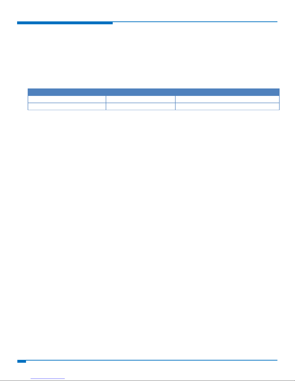
Universal Socket
MT-SMI-DK Developer Guide
Page 2

LEGAL NOTICES AND CONTACT INFORMATION
Universal Socket Developer Guide
2
Universal SocketModem Developer Guide
Cellular SocketModems
MTSMC-G2
MTSMC-G3
MTSMC-H5
MTSMC-C1
MTSMC-C2
MTSMC-LEU1
MTSMC-H3
MTSMC-EV3
MTSMC-LAT1
MTSMC-EV2
MTSMC-E1
MTSMC-LVW2
Analog SocketModems
MT9234SMI
MT5692SMI
MT2492SMI
Embedded Device Servers
MT100SEM-IP
MTS2BTSMI
S000342, Version V
Use Rev S for all builds of the following devices. Consult model specific Device Guides for build options. If you have a older SocketModem, contact
Multi-Tech for documentation.
Copyright
This publication may not be reproduced, in whole or in part, without the specific and express prior written permission signed by an executive officer of
Multi-Tech Systems, Inc. All rights reserved. Copyright © 2017 by Multi-Tech Systems, Inc.
Multi-Tech Systems, Inc. makes no representations or warranties, whether express, implied or by estoppels, with respect to the content, information,
material and recommendations herein and specifically disclaims any implied warranties of merchantability, fitness for any particular purpose and noninfringement.
Multi-Tech Systems, Inc. reserves the right to revise this publication and to make changes from time to time in the content hereof without obligation of
Multi-Tech Systems, Inc. to notify any person or organization of such revisions or changes.
Trademarks
Multi Tech, SocketModem, SocketWireless, Universal IP, SocketEthernet IP and the Multi-Tech logo are registered trademarks of Multi-Tech Systems, Inc.
All other brand and product names are trademarks or registered trademarks of their respective companies.
Legal Notices
The Multi-Tech products are not designed, manufactured or intended for use, and should not be used, or sold or re-sold for use, in connection with
applications requiring fail-safe performance or in applications where the failure of the products would reasonably be expected to result in personal injury
or death, significant property damage, or serious physical or environmental damage. Examples of such use include life support machines or other life
preserving medical devices or systems, air traffic control or aircraft navigation or communications systems, control equipment for nuclear facilities, or
missile, nuclear, biological or chemical weapons or other military applications (“Restricted Applications”). Use of the products in such Restricted
Applications is at the user’s sole risk and liability.
MULTI-TECH DOES NOT WARRANT THAT THE TRANSMISSION OF DATA BY A PRODUCT OVER A CELLULAR COMMUNICATIONS NETWORK WILL BE
UNINTERRUPTED, TIMELY, SECURE OR ERROR FREE, NOR DOES MULTI-TECH WARRANT ANY CONNECTION OR ACCESSIBILITY TO ANY CELLULAR
COMMUNICATIONS NETWORK. MULTI-TECH WILL HAVE NO LIABILITY FOR ANY LOSSES, DAMAGES, OBLIGATIONS, PENALTIES, DEFICIENCIES, LIABILITIES,
COSTS OR EXPENSES (INCLUDING WITHOUT LIMITATION REASONABLE ATTORNEYS FEES) RELATED TO TEMPORARY INABILITY TO ACCESS A CELLULAR
COMMUNICATIONS NETWORK USING THE PRODUCTS.
The Multi-Tech products and the final application of the Multi-Tech products should be thoroughly tested to ensure the functionality of the Multi-Tech
products as used in the final application. The designer, manufacturer and reseller has the sole responsibility of ensuring that any end user product into
which the Multi-Tech product is integrated operates as intended and meets its requirements or the requirements of its direct or indirect customers. MultiTech has no responsibility whatsoever for the integration, configuration, testing, validation, verification, installation, upgrade, support or maintenance of
such end user product, or for any liabilities, damages, costs or expenses associated therewith, except to the extent agreed upon in a signed written
document. To the extent Multi-Tech provides any comments or suggested changes related to the application of its products, such comments or suggested
changes is performed only as a courtesy and without any representation or warranty whatsoever.
Page 3
LEGAL NOTICES AND CONTACT INFORMATION
3
Universal Socket Developer Guide
Country
By Email
By Phone
Europe, Middle East, Africa:
support@multitech.co.uk
+(44) 118 959 7774
U.S., Canada, all others:
support@multitech.com
(800) 972-2439 or (763) 717-5863
Contacting Multi-Tech
Knowledge Base
The Knowledge Base provides immediate access to support information and resolutions for all Multi-Tech products. Visit
http://www.multitech.com/kb.go.
Support Portal
To create an account and submit a support case directly to our technical support team, visit: https://support.multitech.com
Support
Business Hours: M-F, 9am to 5pm CT
World Headquarters
Multi-Tech Systems, Inc.
2205 Woodale Drive
Mounds View, Minnesota 55112
Phone: 763-785-3500 or 800-328-9717
Fax: 763-785-9874
Warranty
To read the warranty statement for your product, please visit: http://www.multitech.com/warranty.go.
Page 4

CONTENTS
Universal Socket Developer Guide
4
Contents
Chapter 1 – Embedded Solutions ................................................................................................................................7
Universal Socket Connectivity Features .............................................................................................................................. 7
Universal IP ......................................................................................................................................................................... 7
Developer Documentation .................................................................................................................................................. 7
The Universal Socket Design ............................................................................................................................................... 8
Embedded Modem and Device Servers .............................................................................................................................. 9
Embedded Cellular Modems........................................................................................................................................... 9
Embedded Analog Modems ............................................................................................................................................ 9
Embedded Device Servers .............................................................................................................................................. 9
Universal Developer Kit Contents ..................................................................................................................................... 10
Attaching Power Supply Blades ........................................................................................................................................ 10
Chapter 2 – Universal Socket Pinout ......................................................................................................................... 12
Pinout Diagrams ................................................................................................................................................................ 12
Universal SocketModem Pinout........................................................................................................................................ 12
Chapter 3 – Universal Design Considerations ............................................................................................................ 16
Noise Suppression Design Considerations ........................................................................................................................ 16
PC Board Layout Guidelines .............................................................................................................................................. 16
User accessible areas .................................................................................................................................................... 16
Electromagnetic Interference (EMI) Considerations ........................................................................................................ 17
Electrostatic Discharge Control ......................................................................................................................................... 17
USB Design Considerations ............................................................................................................................................... 18
Phone Line Warning Statement for the Developer Board ................................................................................................ 18
Mounting Hardware and Tooling Holes ............................................................................................................................ 18
Soldering ........................................................................................................................................................................... 18
Chapter 4 – Developer Board and Schematics ........................................................................................................... 19
SocketModem Developer Board ....................................................................................................................................... 19
SocketModem Developer Board Block Diagram ............................................................................................................... 21
Developer Board Schematics ............................................................................................................................................ 22
Board Components ........................................................................................................................................................... 29
Installing a Universal Socket Communications Device onto the Board ............................................................................ 30
Installing a SIM Card in a Device ....................................................................................................................................... 30
Chapter 5 – Safety Notices and Warnings .................................................................................................................. 31
Cellular Safety ................................................................................................................................................................... 31
RF Safety ....................................................................................................................................................................... 31
Interference with Pacemakers and Other Medical Devices ......................................................................................... 32
Vehicle Safety ................................................................................................................................................................ 32
Device Maintenance ..................................................................................................................................................... 33
Page 5

CONTENTS
5
Universal Socket Developer Guide
User Responsibility ........................................................................................................................................................ 33
Analog Telecom Safety Warnings ..................................................................................................................................... 33
Chapter 6 – Labeling Requirements .......................................................................................................................... 34
Cellular Approvals and Labeling Requirements ................................................................................................................ 34
Approvals and Certification .......................................................................................................................................... 34
Analog Labeling Requirements ......................................................................................................................................... 36
United States Labeling Requirements (for Dial-Up Modems) ...................................................................................... 36
Canadian Labeling Requirements (for Dial-Up Modems) ............................................................................................. 37
Chinese Labeling Requirement ......................................................................................................................................... 40
Chapter 7 – Regulatory Information.......................................................................................................................... 41
Telecom Approvals for Analog Modems ........................................................................................................................... 41
Country/Region-Specific Statements ................................................................................................................................ 41
EMC, Safety, and R&TTE Directive Compliance ............................................................................................................ 41
International Modem Restrictions ................................................................................................................................ 42
47 CFR Part 15 Regulation Class B Devices ................................................................................................................... 42
EMC Requirements for Industry Canada ...................................................................................................................... 42
47 CFR Part 68 Telecom ................................................................................................................................................ 43
South African Statement ............................................................................................................................................... 44
Thailand Approval for MT9234SMI and MT5692SMI ................................................................................................... 44
New Zealand Telecom Warning Notice ........................................................................................................................ 44
Brazil Approval for the MT9234SMI.............................................................................................................................. 45
Russian Statement ........................................................................................................................................................ 45
Korea Class B Statement ............................................................................................................................................... 46
Japan Requirements ..................................................................................................................................................... 46
Other Countries ............................................................................................................................................................ 46
Waste Electrical and Electronic Equipment Statement .................................................................................................... 47
WEEE Directive .............................................................................................................................................................. 47
Instructions for Disposal of WEEE by Users in the European Union ............................................................................. 47
REACH Statement .............................................................................................................................................................. 48
Registration of Substances ............................................................................................................................................ 48
Substances of Very High Concern (SVHC) ..................................................................................................................... 48
Restriction of the Use of Hazardous Substances (RoHS) .................................................................................................. 49
Information on HS/TS Substances According to Chinese Standards ................................................................................ 50
Information on HS/TS Substances According to Chinese Standards (in Chinese) ............................................................ 51
依照中国标准的有毒有害物质信息 ........................................................................................................................... 51
Chapter 8 – Antennas, Cables, and GPS ..................................................................................................................... 52
Antenna System for Cellular Devices ................................................................................................................................ 52
PTCRB Antenna Requirements...................................................................................................................................... 52
Authorized Antennas .................................................................................................................................................... 52
Page 6

CONTENTS
Universal Socket Developer Guide
6
HSPA / UMTS Antenna Requirements/Specifications .................................................................................................. 52
EV-DO and CDMA Antenna Requirements/Specifications ........................................................................................... 53
GSM Antenna Requirements/Specifications ................................................................................................................ 53
GPS Antenna Requirements/Specifications .................................................................................................................. 53
Bluetooth Antenna Requirements/Specifications ........................................................................................................ 53
Antennas Available from Multi-Tech ............................................................................................................................ 54
Additional Sources of Bluetooth Antennas ................................................................................................................... 55
Coaxial Cable Specifications .............................................................................................................................................. 55
SMA-to-UFL and RSMA-to-UFL Coax Cables ................................................................................................................. 55
SMA-to-MMCX and RSMA-to-MMCX Coax Cable ......................................................................................................... 55
SMA-to-MMCX Connector ............................................................................................................................................ 56
OEM Integration ................................................................................................................................................................ 57
FCC Notes ...................................................................................................................................................................... 57
Host Labeling ................................................................................................................................................................. 58
Antenna Diversity .............................................................................................................................................................. 58
Using Antenna Diversity ................................................................................................................................................ 59
Placing External Antennas ............................................................................................................................................ 59
Placing GPS Antennas ................................................................................................................................................... 59
Selecting Antennas ....................................................................................................................................................... 59
Antenna Approvals and Safety Considerations ............................................................................................................ 59
Diversity and Power Draw ............................................................................................................................................ 59
Global Positioning System (GPS) ....................................................................................................................................... 60
Technical Specifications ................................................................................................................................................ 60
Features ........................................................................................................................................................................ 60
Underwriters Laboratories Required Global Positioning System (GPS) Statement ...................................................... 60
Chapter 9 – Upgrading Modem Firmware ................................................................................................................. 62
Upgrading with the Flash Wizard ...................................................................................................................................... 62
Chapter 10 – Cellular SocketModems ....................................................................................................................... 63
Models and Documentation ............................................................................................................................................. 63
Account Activation for Cellular Devices ............................................................................................................................ 63
Chapter 11 – Analog SocketModems ........................................................................................................................ 64
Models and Documentation ............................................................................................................................................. 64
Recommended Parts for Analog SocketModems ............................................................................................................. 64
Telecom ......................................................................................................................................................................... 65
Chapter 12 – Embedded Device Servers .................................................................................................................... 66
Models and Documentation ............................................................................................................................................. 66
Index ....................................................................................................................................................................... 67
Page 7

CHAPTER 1 – EMBEDDED SOLUTIONS
7
Universal Socket Developer Guide
Chapter 1 – Embedded Solutions
Universal Socket Connectivity Features
Get to market quickly with Multi-Tech's pre-approved and ready-to-integrate embedded device networking
solutions with Universal Socket connectivity and Universal IP. Once deployed, your initial design and host
application can quickly adjust to new technologies, essentially future-proofing your solution.
Multi-Tech's Universal Socket offers a flexible architecture that allows you to use one system design and populate
it with your connectivity module of choice.
Interchangeable socket device
Provides cellular, Ethernet, PSTN or Bluetooth network access
Global approvals
Quick-to-market
Easy migration to future technologies, simply upgrade your connectivity module and keep your product
current and design intact
Universal IP
Multi-Tech’s Universal IP stack consists of a common set of TCP/IP networking protocols and M2M applications
implemented using a standard AT command interface. Universal IP provides developers a common programming
interface effectively future proofing their application as new cellular technologies are introduced.
Developer Documentation
Download the documentation from www.multitech.com/support.go. Search on your model to access
documentation for that device.
Universal Socket Developer Guide – This document. Provides an overview, safety and regulatory
information, design considerations, schematics, and general device information.
Device Guides – Provides model-specific specifications and developer information.
AT Command Guides – Device specific AT command reference guides.
USB Driver Installation Guide – Provides steps for installing USB drivers.
Fax Commands – Class 1 and Class 2 commands are supported by some analog modems. Consult the Device
Guide to determine which command set is supported by your device.
Page 8
CHAPTER 1 – EMBEDDED SOLUTIONS
Universal Socket Developer Guide
8
The Universal Socket Design
Each pin on a SocketModem corresponds to a particular function. The universal socket design provides a universal
location for each pin. This allows each SocketModem to be used in a common board. Refer to Universal Socket
Pinout for pinout details.
Page 9
CHAPTER 1 – EMBEDDED SOLUTIONS
9
Universal Socket Developer Guide
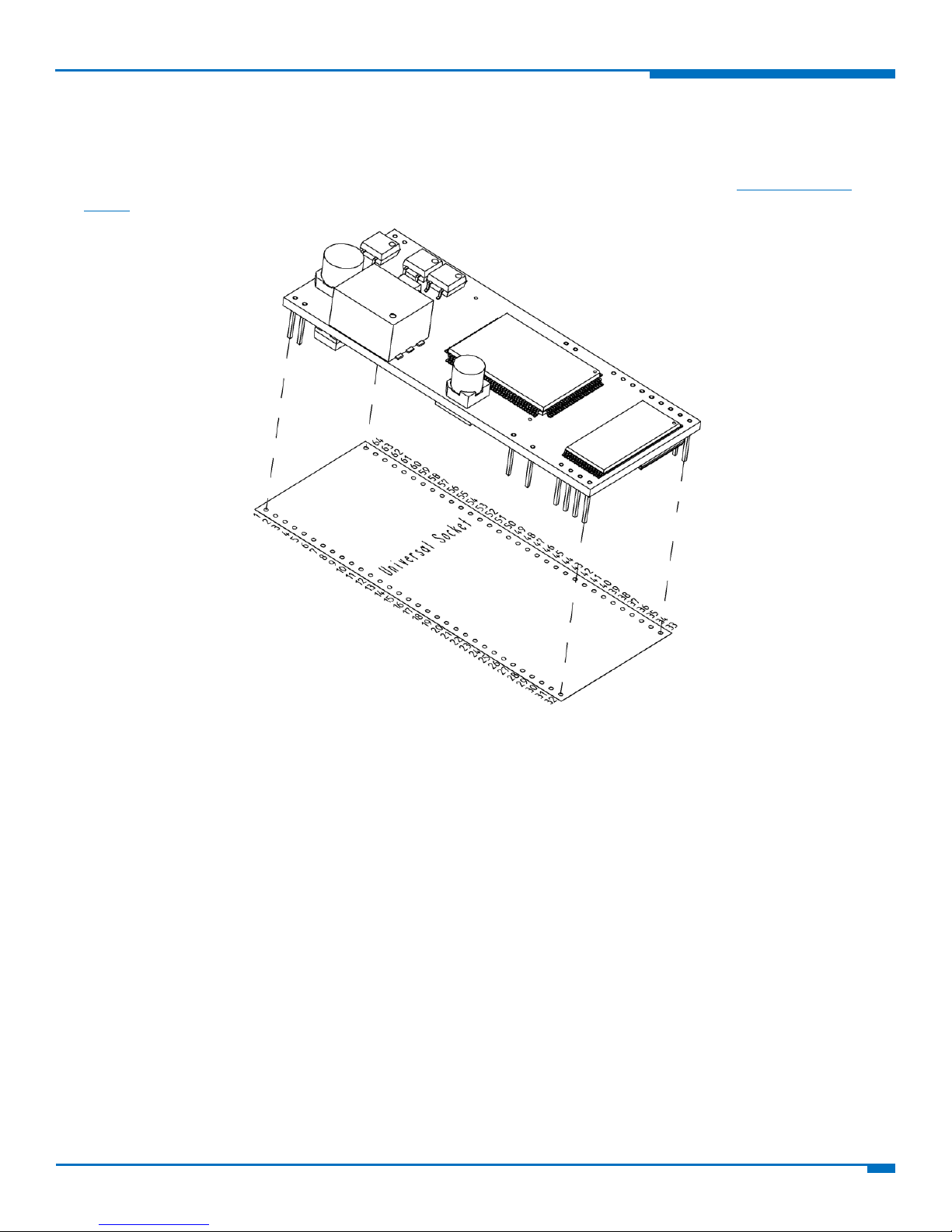
SocketModem iCell
Complete, ready-to-integrate 2G and 3G, GSM and CDMA intelligent cellular modems
using Multi-Tech's Universal Socket design and Universal IP stack for
automatic/persistent connectivity and enhanced M2M (machine-to-machine)
functionality. Models available with GPS tracking capability.
SocketModem Cell
Complete, ready-to-integrate 2G and 3G, GSM, CDMA, and LTE embedded cellular
modem’s using Multi-Tech's Universal Socket design.
SocketModem EDGE
A complete, ready-to-integrate EDGE Class 12 embedded cellular modem using MultiTech's Universal Socket design.
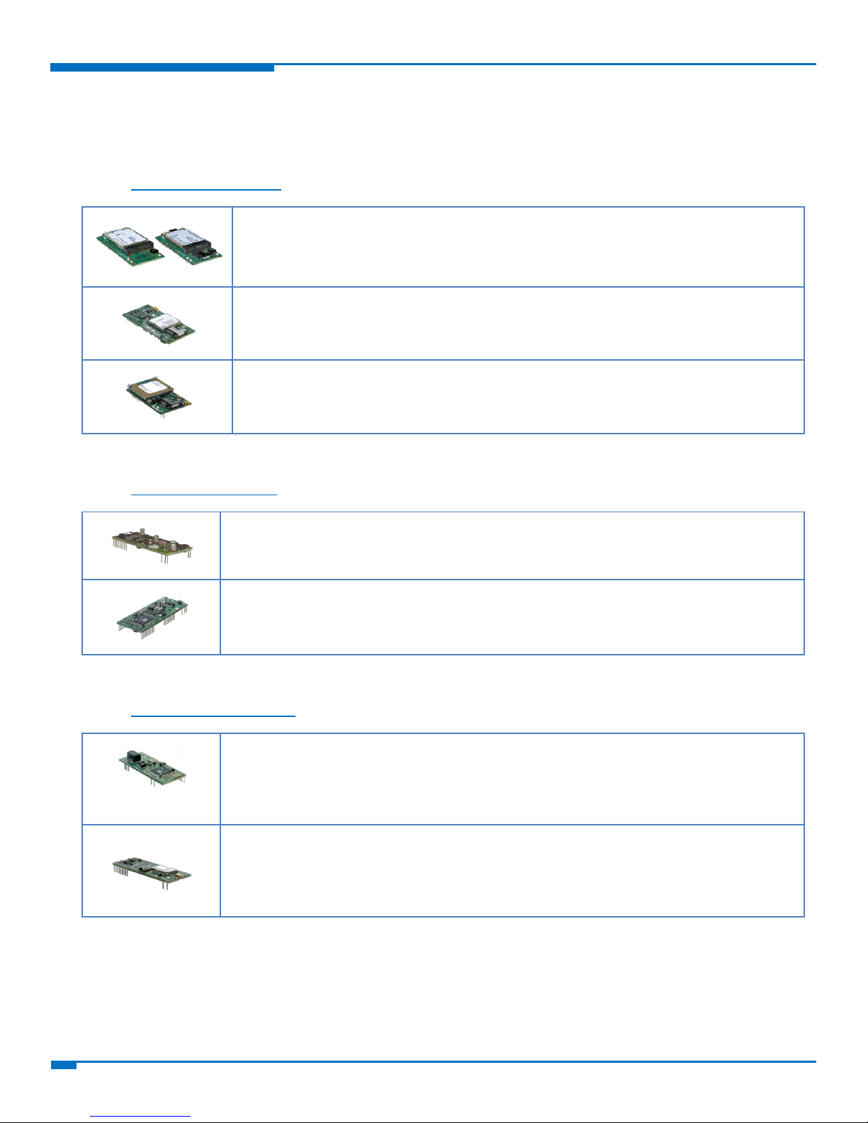
SocketModem
Complete, ready-to-integrate data/fax analog embedded modems using MultiTech's Universal Socket design and telecom approved in more than 50 countries.
SocketModem IP
A complete, V.92 intelligent modem that creates Internet-ready devices by
integrating modem functionality and a complete TCP/IP protocol stack into a single
Universal Socket design.
SocketEthernet IP
Intelligent serial-to-Ethernet device server connects serial devices to an IP network
via a 10/100BaseT Ethernet interface to enable IP networking into virtually any
device allowing remote monitoring, control and configuration. Models available with
medical and high voltage isolation.
SocketWireless
Bluetooth
Complete, ready-to-integrate embedded serial-to-Bluetooth® device server provides
secure wireless connections between a host and peripheral device. Supports pointto-point and multi-point communications allowing wireless data transfers up to 100
meters.
Embedded Modem and Device Servers
Embedded Cellular Modems
Refer to Cellular SocketModems for details about specific models and related documentation.
Embedded Analog Modems
Refer to Analog SocketModems for details about specific models and related documentation.
Embedded Device Servers
Refer to Embedded Device Servers for details about specific models and related documentation.
Page 10
CHAPTER 1 – EMBEDDED SOLUTIONS
Universal Socket Developer Guide
10
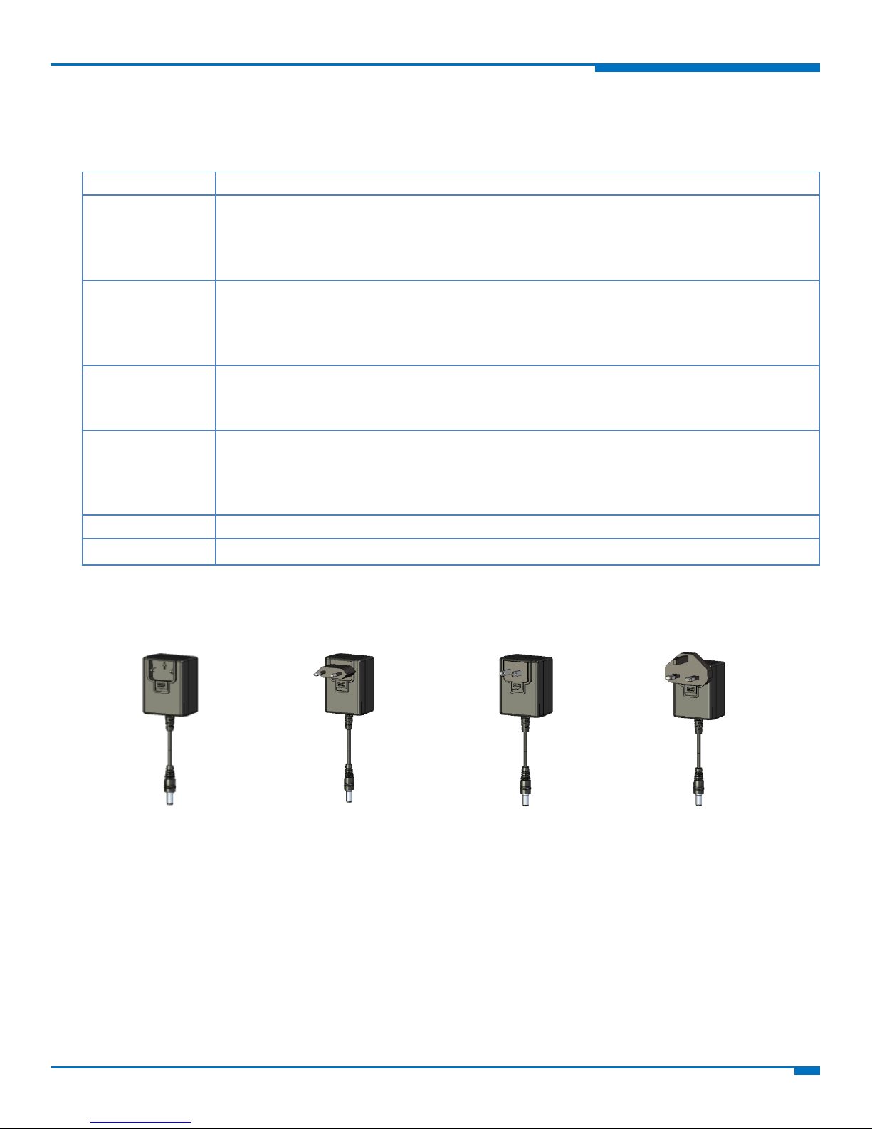
Universal Developer Kit Contents
Developer Board
One MTSMI-UDK Developer Board
Power Supply
One 100-240V 9V-1.7A power supply with removable blades
One US blade/plug
One EURO blade/plug
One UK blade/plug
Cables
One RS-232 DB9F-DB25M serial cable
One RJ-11 phone cable
One RJ-45 Ethernet cable
One USB cable
Antennas
Two hepta band antenna for cellular modems
One 2.4GHz, ½ WAVE antenna with reverse polarity for Bluetooth devices
One GPS antenna
Antenna Cables
One SMA-to-MMCX antenna cable for cellular antennas
Three SMA-to-UFL antenna cables one for select cellular antennas
One for GPS antennas
One RSMA-to-MMCX antenna cable for Bluetooth antennas
Customer Notices
Modem activation notice
Additional
One promotional screwdriver
Power Supply No Blades
Power Supply with EU blade
Power Supply with NAM blade
Power Supply with UK blade
Your Universal Developer Kit (MTSMI-UDK) includes the following:
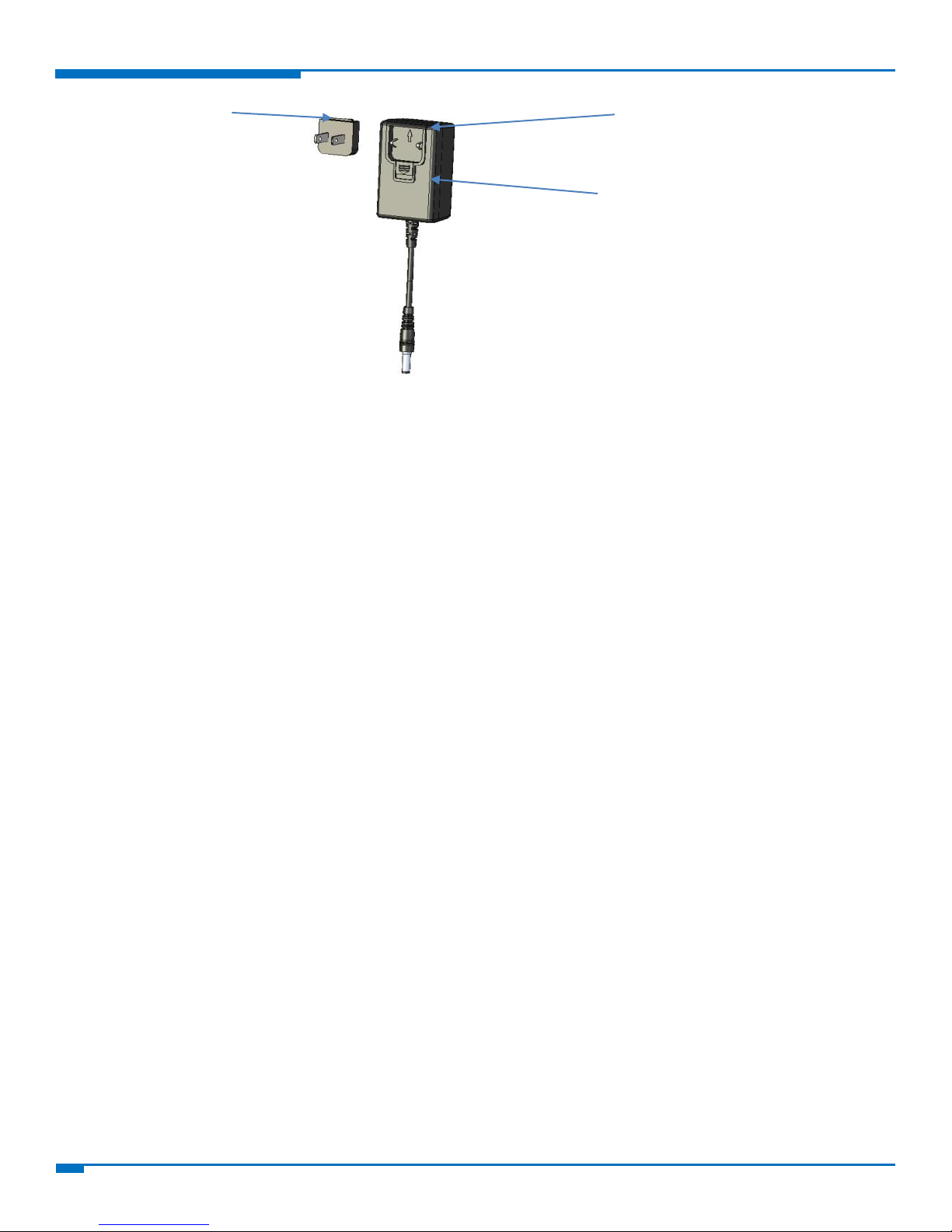
Attaching Power Supply Blades
Power Supply and Blades
To attach a power supply blade:
1. Remove the power supply cover (not shown). To do this, slide the lock down and hold it while you lift off
the cover.
2. Insert the latch on the blade into the notch on the power supply.
3. Slide the lock down and hold it while you press the blade in place.
Page 11
CHAPTER 1 – EMBEDDED SOLUTIONS
11
Universal Socket Developer Guide
Latch Notch
Sliding Lock
Page 12

CHAPTER 2 – UNIVERSAL SOCKET PINOUT
Universal Socket Developer Guide
12
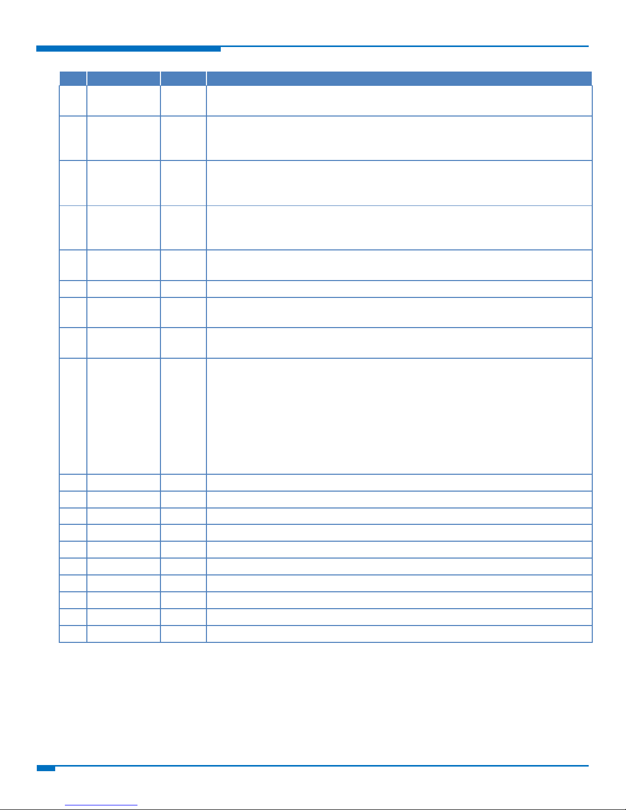
Chapter 2 – Universal Socket Pinout
Pin
Signal Name
In/Out
Description
1
Tip
I/O
Tip Signal from Telco. Tip connection to the phone line (RJ-11 Pin 4). The
SocketModem is Tip/Ring polarity insensitive.
2
Ring
I/O
Ring Signal from Telco. Ring connection to the phone line (RJ-11 Pin 3). The
SocketModem is Tip/Ring polarity insensitive.
3
Safety Void
N/A
Safety Clearance. 2.5 mm is required between TNV circuits and SELV circuits.
4
TX+ O Transmit Outputs (TX+ and TX-). Differential transmit outputs for Ethernet.
5
TX- O Transmit Outputs (TX+ and TX-). Differential transmit outputs for Ethernet.
6
RX- I Receive Inputs. Differential receive input pins for Ethernet. Dummy pin for
MT810SWM-IP.
7
RX+ I Receive Inputs. Differential receive input pins for Ethernet.
8
Safety Void
N/A
Safety Clearance. 2.5 31mm is required between TNV circuits and SELV circuits.
9
Dummy
Dummy pin for EDGE.
Pinout Diagrams
Universal SocketModem Pinout
Note:
Some modems do not include all the pins shown above. Refer to your model’s Device Guide for model
specific pinout information.
Page 13
CHAPTER 2 – UNIVERSAL SOCKET PINOUT
13
Universal Socket Developer Guide
Pin
Signal Name
In/Out
Description
10
Unused
N/A
Reserved for future use.
11
Unused
N/A
Reserved for future use.
12
Unused
N/A
Reserved for future use.
13
Unused
N/A
Reserved for future use.
14
Unused
N/A
Reserved for future use.
15
GPS-SDI
I
GPS Data In.
16
GPS-SDO
O
GPS Data Out.
17
GPS-PPS
GPS Pulse per Second.
18
SPI_CLK
Serial Peripheral Interface custom factory option.
19
SPI_MISO
O
Serial Peripheral Interface custom factory option.
20
SPI_MOSI
I
Serial Peripheral Interface custom factory option.
21
SPI_CS0
Serial Peripheral Interface custom factory option.
22
MIC+
I
Microphone positive input. See individual Device Guides for microphone details.
23
MIC-
I
Microphone negative input. See individual Device Guides for microphone details.
24
-RESET*
I
Device Reset (with pull-up). The active low –RESET input resets the device logic
and returns the configuration of the device to the original factory default values or
"stored values" in the NVRAM. –RESET is tied to VCC through a time-constant
circuit for “Power-on-Reset” functionality. See individual Device Guides for
timings.
A Design Consideration
Allowing the host processor to control the SocketModem’s RESET line allows the
host to reset the device if it fails to respond normally. Resetting the SocketModem
returns it to a known functional state.
25
USB_VBUS
I
USB Voltage Sense. Senses the voltage level of the USB to determine if the bus is
available.
26
GND
GND
Logic Ground.
27
USB_DP
I/O
USB Data Positive. Positive pin of the USB data pair.
28
USB_DN
I/O
USB Data Negative. Negative pin of the USB data pair.
29
LED DCD
O
DCD (Active High). Output from 74LCX14 with a 1000 Ohms resistor in series.
SocketWireless Bluetooth (MTS2BTSMI): When lit, indicates a connection. No
series resistor.
30
LED RX
O
RX (Active High). Output from 74LCX14 with a 1000 Ohms resistor in series.
SocketWireless Bluetooth (MTS2BTSMI): No series resistor.
31
LED DTR
O
DTR (Active High). Output from 74LCX14 with a 1000 Ohms resistor in series.
SocketWireless Bluetooth (MTS2BTSMI): No series resistor.
32
LED TX
O
TX (Active High). Output from 74LCX14 with a 1000 Ohms resistor in series.
SocketWireless Bluetooth (MTS2BTSMI): No series resistor.
33
–RTS
I
Request to Send (Active Low). –RTS is controlled by the DTE to indicate whether
or not the DTE is ready to receive data. –RTS ON (low) indicates that the DTE is
ready to receive data from the modem on RXD. –RTS OFF indicates to the
SocketModem that it should not transfer data on the RXD.
Note: When the –RTS pin is not in use, it should be tied low.
Page 14
CHAPTER 2 – UNIVERSAL SOCKET PINOUT
Universal Socket Developer Guide
14
Pin
Signal Name
In/Out
Description
34
–RXD
O
Received Data. The SocketModem uses the RXD line to send data to the DTE and
to send SocketModem responses to the DTE. In command mode, –RXD data
presents the SocketModem responses to the DTE. SocketModem responses take
priority over incoming data when the two signals are in competition for –RXD.
When no data is transmitted, the signal is held in mark condition.
35
–TXD
I
Transmitted Data. The DTE uses the –TXD line to send data to the SocketModem
for transmission or to transmit commands to the SocketModem. The DTE holds
this circuit in mark state when no data is being transmitted or during intervals
between characters.
36
–RI
O
RING (Active Low). Incoming ring signal from phone.
Ring Indicate. –RI output ON (low) indicates the presence of an ON segment of a
ring signal on the telephone line. The modem will not go off-hook when –RI is
active; the modem waits for –RI to go inactive before going off-hook.
SocketWireless Bluetooth (MTS2BTSMI): Strobes 1/sec for slave indication.
37
–DSR
O
Data Set Ready (Active Low). –DSR indicates SocketModem status to the DTE. –
DSR OFF (high) indicates that the DTE is to disregard all signals appearing on the
interchange circuits except Ring Indicator (–RI). It reflects the status of the local
data set and does not indicate an actual link with any remote data equipment.
38
–CTS
O
Clear to Send (Active Low). –CTS is controlled by the SocketModem to indicate
whether or not the SocketModem is ready to transmit data. –CTS ON indicates to
the DTE that signals on TXD will be transmitted. –CTS OFF indicates to the DTE that
it should not transfer data on TXD.
39
–DCD
O
Data Carrier Detect (Active Low). –DCD output is ON (low) when a data
connection is established and the SocketModem is ready to send/receive data.
40
–DTR
I
Data Terminal Ready (Active Low). The –DTR input is turned ON (low) when the
DTE is ready to communicate. –DTR ON prepares the modem to be connected,
and, once connected, maintains the connection. –DTR OFF places the modem in
the disconnect state under control of the &Dn and &Qn commands.
Note: When the –DTR pin is not in use, it should be tied low.
41
GND
GND
Logic Ground.
42
SPK-
O
Cellular GPRS, CDMA, and EDGE. Negative analog speaker output.
43
SPK+
O
Cellular GPRS, CDMA, and EDGE. Positive analog speaker output.
44
PCM_DO
O
Digital voice custom factory option.
45
PCM_DI
I
Digital voice custom factory option.
46
PCM_FS
O
Digital voice custom factory option.
47
PCM_CLK
O
Digital voice custom factory option.
48
GPIO1
I/O
General Purpose Input/Output. User-configurable input or output pin. 2
49
GPIO1
I/O
General Purpose Input/Output. User-configurable input or output pin. 2
50
GPIO1
I/O
General Purpose Input/Output. User-configurable input or output pin. 2
51
GPIO1
I/O
General Purpose Input/Output. User-configurable input or output pin. 2
52
DBTX/GPIO
O
Not currently used.
53
DBRX/GPIO
I
Not currently used.
54
GPIO
N/A
Reserved for future use.
55
Heartbeat
N/A
Reserved for future use.
Page 15
CHAPTER 2 – UNIVERSAL SOCKET PINOUT
15
Universal Socket Developer Guide
Pin
Signal Name
In/Out
Description
56
–LED FDX
O
LED Full Duplex (Active Low). LED Output. During normal operation, this pin lights
the FDX LED to indicate a full duplex mode.
57
–LED ACT
O
LED Active (Active Low). LED Output. During normal operation, this pin lights the
Activity LED when transmitting or receiving. It flashes at a rate of 50ms high and
50ms low when active.
58
–LEDLINK
O
LED LINK (Active Low). LED Output. During normal operation, this pin lights the
LINK LED to indicate a good link is detected.
Refer the individual Device Guide for PIN 58 LED Mode details.
59
–LEDCOL
O
LED Collision (Active Low). LED Output. During normal operation, this pin lights
the COL LED to indicate a collision. It flashes at 50ms high and 50ms low when
active.
60
–LEDSPD
O
LED Speed (Active Low). LED Output. During normal operation, this pin lights the
SPEED LED to indicate 100Mbps is selected.
61
VCC
PWR
DC Input Power. 3.3V or 5VDC power, depending upon the build.
62
MICV
I
Single-Ended Microphone. Single-ended microphone input for dial-up
SocketModem speakerphone and TAM functions.
63
AGND
GND
Analog Ground. Analog ground is tied common with DGND on the SocketModem.
To minimize potential ground noise issues, connect audio circuit return to AGND.
64
SPKR
O
Speaker. Dual purpose output for call progress signals or speakerphone functions.
Call Progress signaling on MT5692SMI and MT2492SMI is a square wave output
that can be optionally connected to a low-cost single-ended speaker; e.g., a
sounducer or an analog speaker circuit.
Call progress on the MT9234SMI is an analog output.
Speakerphone Output on the MT5692SMI is under the control of +FCLASS. This is
a single-ended analog output. SPKR is tied directly to the CODEC. One side of a
differential AC output coupled through a 6.8K ohm resistor and capacitor.
65
Unused
N/A
Reserved for future use.
66
Unused
N/A
Reserved for future use.
67
Unused
N/A
Reserved for future use.
68
Unused
N/A
Reserved for future use.
69
Unused
N/A
Reserved for future use.
70
Unused
N/A
Reserved for future use.
71
Unused
N/A
Reserved for future use.
72
Unused
N/A
Reserved for future use.
73
Unused
N/A
Reserved for future use.
74
Unused
N/A
Reserved for future use.
1
GPIO pins can be configured using the Universal IP AT Commands. Refer to the Universal IP AT Commands
Reference Guide.
2
For MTSMC-H3-MI-IP, MTSMC-EV2-MI-IP, MTSMC-EV2-MI-GP, MTSMC-H5-MI, MTSMC-H5-MI-GP, MTSMC-EV3-
MI and MTSMC-EV-MI-GP only.
Page 16

CHAPTER 3 – UNIVERSAL DESIGN CONSIDERATIONS
Universal Socket Developer Guide
16
Chapter 3 – Universal Design Considerations
Noise Suppression Design Considerations
Adhere to engineering noise-suppression practices when designing a printed circuit board (PCB) containing the
SocketModem. Noise suppression is essential to the proper operation and performance of the modem and
surrounding equipment.
Any OEM board design that contains the SocketModem should consider both on-board and off-board generated
noise that can affect digital signal processing. Both on-board and off-board generated noise that is coupled onboard can affect interface signal levels and quality. Noise in frequency ranges that affect modem performance is of
particular concern.
On-board generated electromagnetic interference (EMI) noise that can be radiated or conducted off-board is
equally important. This type of noise can affect the operation of surrounding equipment. Most local government
agencies have stringent certification requirements that must be met for use in specific environments.
Proper PC board layout (component placement, signal routing, trace thickness and geometry, etc.) component
selection (composition, value, and tolerance), interface connections, and shielding are required for the board
design to achieve desired modem performance and to attain EMI certification.
Other aspects of proper noise-suppression engineering practices are beyond the scope of this guide. Consult noise
suppression techniques described in technical publications and journals, electronics and electrical engineering text
books, and component supplier application notes.
PC Board Layout Guidelines
In a 4-layer design, provide adequate ground plane covering the entire board. In 4-layer designs, power and
ground are typically on the inner layers. All power and ground traces should be 0.05 inches wide.
The recommended hole size for the SocketModem pins is 0.036 in. +/-0.003 in. in diameter. Use spacers to hold
the SocketModem vertically in place during the wave solder process.
All creepages and clearances for the SocketModem have been designed to meet requirements of safety standards
EN60950 or EN60601. The requirements are based on a working voltage of 125V or 250V. When implementing the
recommended DAA* circuit interface in a third party design, strictly follow all creepage and clearance
requirements in order to meet safety standards. The third party safety design must be evaluated by the
appropriate national agency per the required specification.
User accessible areas
Based on where the third party design is to be marketed, sold, or used, it may be necessary to provide an
insulating cover over all TNV exposed areas. Consult with the recognized safety agency to determine the
requirements.
Note:
Even if the recommended design considerations are followed, there are no guarantees that a particular
system will comply with all the necessary regulatory requirements. It is imperative that specific designs be
completely evaluated by a qualified/recognized agency.
*DAA stands for Data Access Arrangement. DAA is the telephone line interface of the SocketModem.
Page 17

CHAPTER 3 – UNIVERSAL DESIGN CONSIDERATIONS
17
Universal Socket Developer Guide
Electromagnetic Interference (EMI) Considerations
The following guidelines are offered specifically to help minimize EMI generation. Some of these guidelines are the
same as, or similar to, the general guidelines. To minimize the contribution of the SocketModem-based design to
EMI, you must understand the major sources of EMI and how to reduce them to acceptable levels.
Keep traces carrying high frequency signals as short as possible.
Provide a good ground plane or grid. In some cases, a multilayer board may be required with full layers for
ground and power distribution.
Decouple power from ground with decoupling capacitors as close to the SocketModem power pins as
possible.
Eliminate ground loops, which are unexpected current return paths to the power source and ground.
Decouple the telephone line cables at the telephone line jacks. Typically, use a combination of series
inductors, common mode chokes, and shunt capacitors. Methods to decouple telephone lines are similar to
decoupling power lines; however, telephone line decoupling may be more difficult and deserves additional
attention. A commonly used design aid is to place footprints for these components and populate as
necessary during performance/EMI testing and certification.
Decouple the power cord at the power cord interface with decoupling capacitors. Methods to decouple
power lines are similar to decoupling telephone lines.
Locate high frequency circuits in a separate area to minimize capacitive coupling to other circuits.
Locate cables and connectors to avoid coupling from high frequency circuits.
Lay out the highest frequency signal traces next to the ground grid.
If using a multilayer board design, make no cuts in the ground or power planes and be sure the ground plane
covers all traces.
Minimize the number of through-hole connections on traces carrying high frequency signals.
Avoid right angle turns on high frequency traces. Forty-five degree corners are good; however, radius turns
are better.
On 2-layer boards with no ground grid, provide a shadow ground trace on the opposite side of the board to
traces carrying high frequency signals. This will be effective as a high frequency ground return if it is three
times the width of the signal traces.
Distribute high frequency signals continuously on a single trace rather than several traces radiating from one
point.
Electrostatic Discharge Control
Handle all electronic devices with certain precautions to avoid damage due to the static charge accumulation.
See the ANSI/ESD Association Standard (ANSI/ESD S20.20-1999) – a document “for the Development of an
Electrostatic Discharge Control for Protection of Electrical and Electronic Parts, Assemblies and Equipment.” This
document covers ESD Control Program Administrative Requirements, ESD Training, ESD Control Program Plan
Technical Requirements (grounding/bonding systems, personnel grooming, protected areas, packaging, marking,
equipment, and handling), and Sensitivity Testing.
Multi-Tech Systems, Inc. strives to follow all of these recommendations. Input protection circuitry has been
incorporated into the Multi-Tech devices to minimize the effect of static buildup, take proper precautions to avoid
exposure to electrostatic discharge during handling.
Page 18

CHAPTER 3 – UNIVERSAL DESIGN CONSIDERATIONS
Universal Socket Developer Guide
18
Multi-Tech uses and recommends that others use anti-static boxes that create a faraday cage (packaging designed
Solder pot temperature:
275C
Preheat zone 1:
135C
Preheat zone 2:
160C
Preheat zone 3:
175C
Belt speed:
35.4 inches per minute
to exclude electromagnetic fields). Multi-Tech recommends that you use our packaging when returning a product
and when you ship your products to your customers.
USB Design Considerations
Multi-Tech recommends consulting Intel's High Speed USB Platform Design Guidelines, Rev. 1.0 for information
about USB signal routing, impedance, and layer stacking. Also:
Shield USB cables with twisted pairs (especially those containing D+/D-).
Use a single 5V power supply for USB devices. Consult your model’s Device Guide for Power Draw section for
current (ampere) requirements.
Route D+/D- together in parallel with the trace spacing needed to achieve 90 ohms differential impedance
for the USB pair and to maintain a 20 mil space from the USB pair and all other signals.
If power is provided externally, use a common ground between the carrier board and SocketModem.
Phone Line Warning Statement for the Developer Board
(Analog only) Use extreme caution when the phone line is installed due to live energized components. Do not
touch any components on the board while the phone line is installed.
Detach the phone line when making modifications to or servicing the developer board.
For other telephone warnings, refer to the Telecom Warnings
Mounting Hardware and Tooling Holes
Refer to individual Device Guide for specific hardware requirements.
Soldering
Multi-Tech uses a wave soldering process:
Preheat zones have top and bottom heaters.
WARNING: Do not wash. Washing may damage the device.
NOTE: Conditions of Acceptability for UL are available upon request at https://support.multitech.com.
Page 19
CHAPTER 4 – DEVELOPER BOARD AND SCHEMATICS
19
Universal Socket Developer Guide
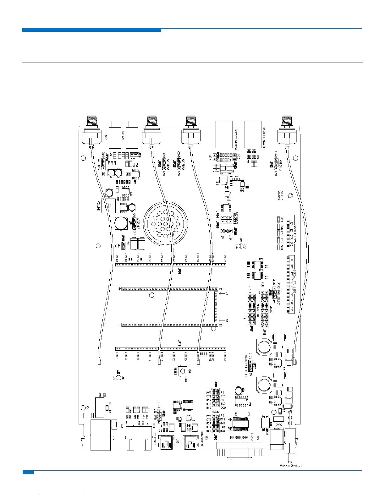
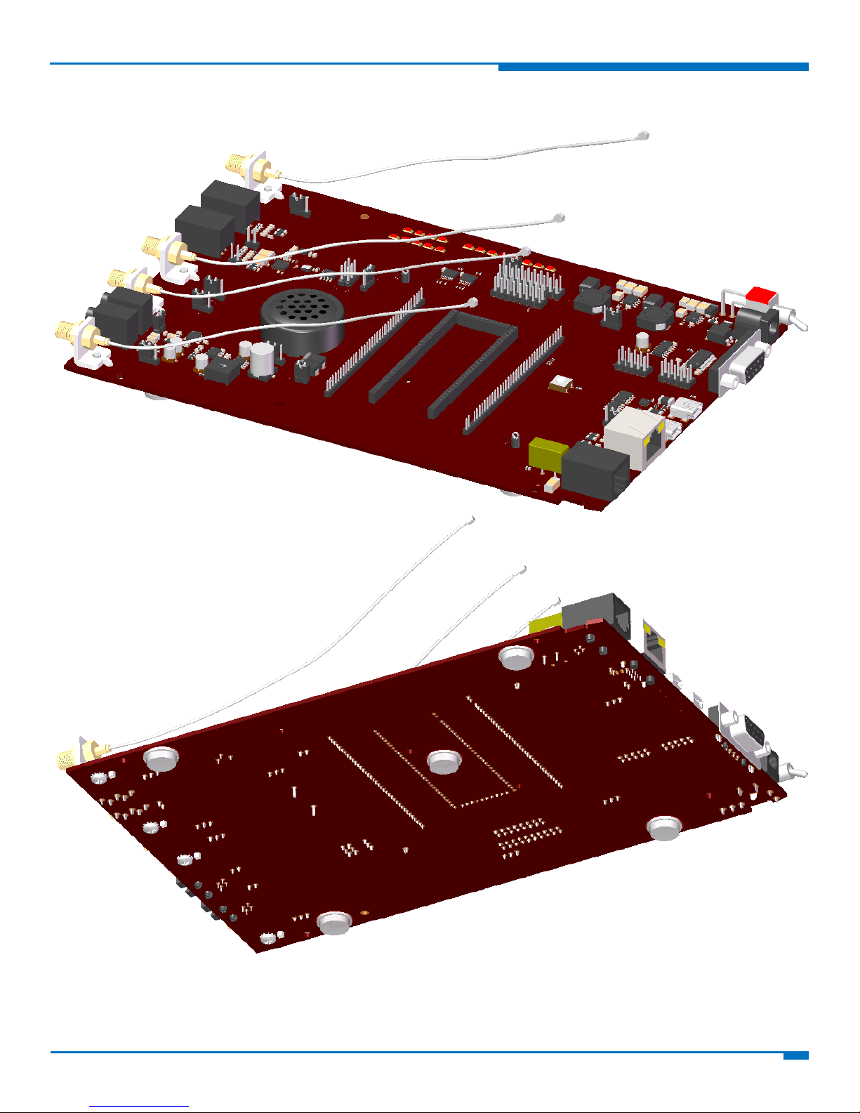
Chapter 4 – Developer Board and Schematics
Note: Third-party components shown in the following drawings are included as examples only.
SocketModem Developer Board
This developer board drawing shows the major board components for all SocketModems.
Page 20
CHAPTER 4 – DEVELOPER BOARD AND SCHEMATICS
Universal Socket Developer Guide
20
Page 21
CHAPTER 4 – DEVELOPER BOARD AND SCHEMATICS
21
Universal Socket Developer Guide
SocketModem Developer Board Block Diagram
Page 22

CHAPTER 4 – DEVELOPER BOARD AND SCHEMATICS
Universal Socket Developer Guide
22
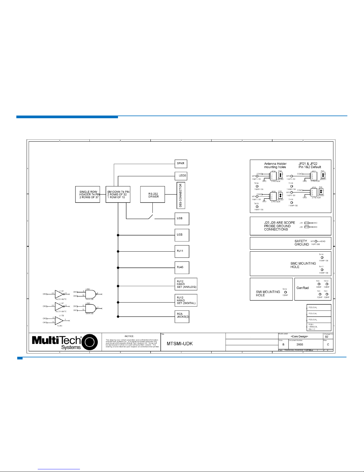
Developer Board Schematics
Page 23

CHAPTER 4 – DEVELOPER BOARD AND SCHEMATICS
23
Universal Socket Developer Guide
Page 24

CHAPTER 4 – DEVELOPER BOARD AND SCHEMATICS
Universal Socket Developer Guide
24
Page 25

CHAPTER 4 – DEVELOPER BOARD AND SCHEMATICS
25
Universal Socket Developer Guide
Page 26

CHAPTER 4 – DEVELOPER BOARD AND SCHEMATICS
Universal Socket Developer Guide
26
Page 27

CHAPTER 4 – DEVELOPER BOARD AND SCHEMATICS
27
Universal Socket Developer Guide
Page 28

CHAPTER 4 – DEVELOPER BOARD AND SCHEMATICS
Universal Socket Developer Guide
28
Page 29

HAPTER 4 – DEVELOPER BOARD AND SCHEMATICS
29
Multi-Tech Systems, Inc. Universal Socket Developer Guide
Schematic
Jumper Label
PCB Label or
Location
Description
J19
Next to
stereo jack.
Allows a stereo jack feed. Default is ON. If ON, then left and right stereo channels
are combined and form a mono channel.
J25& J26
GND LUG
Ground lug.
JP1
Speaker
Mutes the speaker. Default positions are 1 and 2 (speaker is not muted).
JP13
USB PWR
Set either 5V or 3.3V for USB_VBUS line (supplied by the VCC of the USB jack).
JP16
JTAG
JTAG header.
JP17
Mosquito
Mosquito header. If used to debug the SocketModem while using the USB port,
remove the JP13 to disconnect USB_VBUS.
JP18
MOD PWR
Power feed (Vcc) SocketModem module. (X3).
JP19& JP20
Debugging probes pins for SocketModem.
JP21 & JP22
Antenna
Antenna ground select.
JP24 & JP25
Antenna
Antenna ground select.
JP28
Handset
Digital
Digital handset jack, 4 pin connector (not labeled on schematic).
JP49
SPK
Speaker jack header.
JP50
MIC
Microphone jack header.
JP83 & JP84
ATtiny25
ATtiny25 6-pin programmer headers.
JP85
1.8V 5V
Selects operating voltage (1.8v or 5v) for the ATtiny25v micro-controller.
JP87
Board PWR
Select
The 5V/3.3V regulator. Factory default operating voltage is 5V.
Warning:
Verify that the 5V/3.3V jumper matches your SocketModem’s
requirements. If this jumper is set incorrectly, you could damage the
SocketModem and/or Test/Demo board.
Use only the Multi-Tech Systems supplied transformer with the
Test/Demo board. Using any other power source voids the warranty
and will likely damage the Test/Demo board and SocketModem.
JP88
JTAG PWR
Select
Selects operating voltage (5v or 3.3v) for the JTAG.
JP89
SER TL
Testing interface (debugging) for the serial TTL signals.
JP90
RS232
Testing interface (debugging) for the RS-232 signals.
S1
Next to 9VDC
Power Jack
Board input power switch (not labeled on schematic).
S5
RESET
Reset push switch.
Board Components
Jxx indicates jacks.
Page 30

CHAPTER 4 – DEVELOPER BOARD AND SCHEMATICS
Universal Socket Developer Guide
30
Installing a Universal Socket Communications Device onto the
Board
To install a SMI/SMC modem:
1. Align the pin of the universal socket communications device with pin 1 of the universal socket connector
on the board and press firmly.
2. Use the optional antenna lead to connect to the antenna connector on the modem.
Installing a SIM Card in a Device
To install a SIM card:
Install the SIM card into the device’s SIM card holder.
Page 31

CHAPTER 5 – SAFETY NOTICES AND WARNINGS
31
Universal Socket Developer Guide
Chapter 5 – Safety Notices and Warnings
The following safety statements may be used in your product documentation.
Cellular Safety
RF Safety
Due to the possibility of radio frequency (RF) interference, it is important that you follow any special regulations
regarding the use of radio equipment. Follow the safety advice given below.
CAUTION: Maintain a separation distance of at least 20 cm (8 inches) between the transmitter’s antenna and the
body of the user or nearby persons. The modem is not designed for or intended to be used in portable
applications within 20 cm of the user’s body.
Check your local standards regarding safe distances, etc.
Operating your device close to other electronic equipment may cause interference if the equipment is
inadequately protected. Observe any warning signs and manufacturers’ recommendations.
Different industries and businesses restrict the use of cellular devices. Respect restrictions on the use of
radio equipment in fuel depots, chemical plants, or where blasting operations are in process. Follow
restrictions for any environment where you operate the device.
Do not place the antenna outdoors.
Switch OFF your wireless device when in an aircraft. Using portable electronic devices in an aircraft may
endanger aircraft operation, disrupt the cellular network, and is illegal. Failing to observe this restriction
may lead to suspension or denial of cellular services to the offender, legal action, or both.
Switch OFF your wireless device when around gasoline or diesel-fuel pumps and before filling your vehicle
with fuel.
Switch OFF your wireless device in hospitals and any other place where medical equipment may be in use.
Sécurité des fréquences radio
En raison de la possibilité d'interférences de radiofréquence (RF), il est important que vous suiviez une quelconque
réglementation concernant l'utilisation du matériel radio. Suivez les conseils de sécurité ci-dessous.
Attention: Maintenir une distance d'au moins 20 cm (8 po) entre l'antenne du récepteur et le corps de
l'utilisateur ou à proximité de personnes. Le modem n'est pas conçu pour, ou destinés à être
utilisés dans les applications portables, moins de 20 cm du corps de l'utilisateur.
Vérifiez vos normes locales touchant les distances de sécurité, etc..
Fonctionnement de votre appareil à proximité d'autres appareils électroniques peuvent causer des
interférences si l'équipement est insuffisamment protégé. Respectez les panneaux d'avertissement et les
recommandations du fabricant.
Différentes industries et les entreprises limitent l'utilisation des appareils cellulaires. Respectez les
règlements sur l'utilisation des équipements radio dans les dépôts de carburant, les usines chimiques, ou
lorsque des opérations de dynamitage sont en cours. Suivez restrictions pour n'importe quel environnement
où vous utilisez l'appareil.
Ne pas placer l'antenne à l'extérieur.
Éteignez votre appareil sans fil dans un avion. Utilisant des dispositifs électroniques portables dans un avion
peut mettre en danger le fonctionnement de l'avion, peut perturber le réseau cellulaire, et est illégal. Le
Page 32

CHAPTER 5 – SAFETY NOTICES AND WARNINGS
Universal Socket Developer Guide
32
non-respect de cette restriction peut entraîner la suspension ou le refus des services cellulaires au
contrevenant, une action en justice, ou les deux.
Éteignez votre appareil sans fil lorsque autour de l'essence ou pompes diesel-carburant et avant de remplir
votre véhicule avec du carburant.
Éteignez votre appareil sans fil dans les hôpitaux et tout autre endroit où l'équipement médical peut être
utilisé.
Interference with Pacemakers and Other Medical Devices
Potential interference
Radiofrequency energy (RF) from cellular devices can interact with some electronic devices. This is
electromagnetic interference (EMI). The FDA helped develop a detailed test method to measure EMI of implanted
cardiac pacemakers and defibrillators from cellular devices. This test method is part of the Association for the
Advancement of Medical Instrumentation (AAMI) standard. This standard allows manufacturers to ensure that
cardiac pacemakers and defibrillators are safe from cellular device EMI.
The FDA continues to monitor cellular devices for interactions with other medical devices. If harmful interference
occurs, the FDA will assess the interference and work to resolve the problem.
Precautions for pacemaker wearers
If EMI occurs, it could affect a pacemaker in one of three ways:
Stop the pacemaker from delivering the stimulating pulses that regulate the heart's rhythm.
Cause the pacemaker to deliver the pulses irregularly.
Cause the pacemaker to ignore the heart's own rhythm and deliver pulses at a fixed rate.
Based on current research, cellular devices do not pose a significant health problem for most pacemaker wearers.
However, people with pacemakers may want to take simple precautions to be sure that their device doesn't cause
a problem.
Keep the device on the opposite the side of the body from the pacemaker to add extra distance between
the pacemaker and the device.
Avoid placing a turned-on device next to the pacemaker (for example, don’t carry the device in a shirt or
jacket pocket directly over the pacemaker).
Vehicle Safety
Do not use this device while driving.
Respect national regulations on the use of cellular devices in vehicles.
If incorrectly installed in a vehicle, operating the wireless device could interfere with the vehicle’s
electronics. To avoid such problems, use qualified personnel to install the device. The installer should verify
the vehicle electronics are protected from interference.
Using an alert device to operate a vehicle’s lights or horn is not permitted on public roads.
UL evaluated this device for use in ordinary locations only. UL did NOT evaluate this device for installation in
a vehicle or other outdoor locations. UL Certification does not apply or extend to use vehicles or outdoor
applications or in ambient temperatures above 40° C.
Page 33

CHAPTER 5 – SAFETY NOTICES AND WARNINGS
33
Universal Socket Developer Guide
Device Maintenance
Do not attempt to disassemble the device. There are no user serviceable parts inside.
Do not expose your device to any extreme environment where the temperature or humidity is high.
Do not expose the device to water, rain, or spilled beverages. It is not waterproof.
Do not place the device alongside computer discs, credit or travel cards, or other magnetic media. The
information contained on discs or cards may be affected by the phone.
Using accessories that Multi-Tech has not authorized or that are not compliant with Multi-Tech’s accessory
specifications may invalidate the warranty.
If the device is not working properly, contact Multi-Tech Technical Support.
User Responsibility
Respect all local regulations for operating your wireless device. Use the security features to block
unauthorized use and theft.
Analog Telecom Safety Warnings
Before servicing, disconnect this product from its power source and telephone network. Also:
Never install telephone wiring during a lightning storm.
Never install a telephone jack in wet locations unless the jack is specifically designed for wet locations.
Use this product with UL and cUL listed computers only.
Never touch uninsulated telephone wires or terminals unless the telephone line has been disconnected at
the network interface.
Use caution when installing or modifying telephone lines.
Avoid using a telephone during an electrical storm. There may be a remote risk of electrical shock from
lightning.
Do not use a telephone in the vicinity of a gas leak.
CAUTION: To reduce the risk of fire, use only 26 AWG or larger UL Listed or CSA Certified telecommunication
line cord.
Avertissements de sécurité télécom analogique
Avant de l'entretien, débrancher ce produit de son réseau d'alimentation et de téléphone. également:
Ne jamais installer du câblage téléphonique pendant un orage électrique.
Ne jamais installer de prises téléphoniques à des endroits mouillés à moins que la prise ne soit conçue pour
de tels emplacements.
Utilisez ce produit avec UL et cUL ordinateurs répertoriés seulement.
Ne jamais toucher fils ou des bornes téléphoniques non isolés à moins que la ligne téléphonique n'ait été
déconnectée au niveau de l'interface réseau.
Faire preuve de prudence au moment d'installer ou de modifier des lignes téléphoniques.
Éviter d'utiliser le téléphone pendant un orage électrique. Il peut y avoir un risque de choc électrique causé
par la foudre.
N'utilisez pas un téléphone à proximité d'une fuite de gaz.
ATTENTION: Pour réduire les risques d’incendie, utiliser uniquement des conducteurs de télécommunications 26
AWG au de section supérleure.
Page 34

CHAPTER 6 – LABELING REQUIREMENTS
Universal Socket Developer Guide
34
Chapter 6 – Labeling Requirements
Host Device Model Identification
Multi-Tech SocketModem
Model Identification
IMEI Number
Cellular Approvals and Labeling Requirements
Note: For MTSMC LTE models, refer to the MTSMC-Lxx Device Guide for labeling requirements.
Approvals and Certification
The Multi-Tech SocketModem is an industry and/or carrier approved modem. In most cases, when integrated and
used with an antenna system that was part of the Multi-Tech modem certification, additional approvals or
certifications are not required for the device you develop as long as the following are met. Note that EV-DO
modems have a few exceptions.
PTCRB Requirements (EDGE, GPRS and HSPA/HSDPA only)
The antenna system cannot be altered.
Model Identification
The Multi-Tech model identification allows the carrier to verify the modem as one of its approved models.
This information is located on the modem's label.
Note: Both the host device and modem include labels. When the cellular carrier asks you to provide the
modem's model identification, give the Multi-Tech cellular model identification, not the host device
model. The ESN or IMEI number on the host device label will match that of the modem.
For C1, C2, and EV3 SocketModems: The modem's MEID (Mobile Equipment Identifier) written in
hexadecimal format is printed under the barcode on the modem.
For EV2: The modem’s ESN (Electronic Serial Number) is printed below the barcode.
For G2, G3, H3, and H5 SocketModems: The modem's 15-character IMEI (International Mobile Equipment
Identity) number is printed on the modem's label.
Example GPRS End Product Label
Note: Actual labels will vary depending on the regulatory approval markings and content.
Page 35

CHAPTER 6 – LABELING REQUIREMENTS
35
Universal Socket Developer Guide
Page 36

CHAPTER 6 – LABELING REQUIREMENTS
Universal Socket Developer Guide
36
Example CDMA C1 SocketModem Label
Multi-Tech Model Identification
Multi-Tech Ordering Part Number
MEID
(On EV2 Devices, the ESN is here.)
Notes:
The label is shown larger than actual size.
Actual labels will vary depending on the regulatory approval markings and content.
Analog Labeling Requirements
United States Labeling Requirements (for Dial-Up Modems)
Telecom requirements apply to analog products only.
Approved terminal equipment (TE) and approved protective circuitry shall prominently display the following
information using the format shown below:
Responsible party or manufacturer
Product Identification
Equipment Code
Ringer Equivalence
Ringer Type
Indication that the product meets the requirements of FCC Part 68
The information required by the first five items shall correspond to the records in the ACTA database of approved
equipment. The required information shall be encoded in the following format:
US: AAAEQ##TXXX
Where:
US: Is a fixed field that indicates the equipment meets all requirements of 47 CFR Part 68, including the
AAA is the responsible party’s Grantee Code obtained previously from the FCC’s Common Carrier Bureau or
EQ Is an equipment code indicating to the Service Provider any special signal handling or billing
requirements published by ACTA.
currently from ACTA.
requirements. The equipment codes are listed in Annex A (normative).
Page 37

CHAPTER 6 – LABELING REQUIREMENTS
37
Universal Socket Developer Guide
## is the Ringer Equivalence Number without a decimal point (e.g. REN of 1.0 = 10, REN of 0.3 = 03). In the
case of a “Z” ringer, ZZ shall appear. In the case of approved equipment without a network interface and
equipment not connecting to circuits with analog ringing supplied then “NA” shall appear.
T is the ringer type letter associated with the Ringer Equivalence Number, in accordance with the technical
requirements. In the case of approved equipment without a network interface and equipment not
connecting to circuits with analog ringing supplied, the letter “N” shall appear.
XXX Is a product identifier, unique when combined with the responsible party’s Grantee Code, of at least
one and up to nine alphanumeric characters (including one or more dashes (-) if desired. A dash shall not
appear as the first or last character nor shall the identifier consist entirely of dashes). The responsible party
shall define this identifier.
Label Physical Characteristics
The required information in the previous section shall be permanently affixed and legible without magnification. It
may be etched, engraved, stamped, indelibly printed, or otherwise permanently marked. Alternatively, the
required information may be permanently marked on a nameplate of metal, plastic or other material fastened to
the enclosure by welding, riveting or with a permanent adhesive. Such a nameplate shall be able to last for the
expected lifetime of the equipment and shall not be readily detachable.
Labeling Continuity and Changes
The labeling content and format requirements in effect when a product was approved shall be effective for the life
of the product. The labeling content and format requirements in effect at approval shall also continue to be
effective for modified products. However, the responsible party shall have the option of conforming a product's
labeling to current content and format requirements at any time.
Other Label Requirements
Place the label in one of the following locations so it can be found after installation:
On an outside surface
Inside a readily available access door or panel
On another readily accessible surface
For example, do not put the label on the rear of a permanently wall-mounted device where it is not readily
accessible.
Canadian Labeling Requirements (for Dial-Up Modems)
The following requirements are established under section 69.3 of the Telecommunications Act for purposes of
section 5 of the Telecommunications Apparatus Regulations.
Registered equipment shall bear the following identifying marks, and the Declaring Party shall ensure that these
marks are permanently affixed to the equipment:
a. The registration number — Specifications of this mark are given in the document: Self-Marking of the
Certification/Registration Number on Terminal Equipment — Application Procedure and Agreement;
and
b. The model identification number under which the product was registered.
A statement of compliance with Industry Canada requirements, such as the one given below, shall accompany
each unit of equipment whether registered under this procedure or previously certified:
This product meets the applicable Industry Canada technical specifications.
Page 38

CHAPTER 6 – LABELING REQUIREMENTS
Universal Socket Developer Guide
38
For terminal equipment intended for connection to loop-start or ground-start interfaces, the Ringer Equivalence
Number (REN) must be calculated as per Section 1.8 of CS-03, Part I. A REN higher than that determined may be
assigned by manufacturers to allow for production variations. The REN must be marked on the terminal
equipment itself or added to the note below. A note similar to the following shall accompany each unit of
equipment whether registered under this procedure or previously certified:
The Ringer Equivalence Number is an indication of the maximum number of devices allowed to be connected
to a telephone interface. The termination on an interface may consist of any combination of devices subject
only to the requirement that the sum of the RENs of all the devices does not exceed five.
Pursuant to section 69.3 of the Telecommunications Act, certified or self-declared TE will bear a valid identifying
certification number or registration number. The marking of the certification or registration number on the
product shall be as follows:
a. TAC holder/DP will be responsible for permanently affixing the certification/registration number on the
TE. The certification/registration number (see example below) identifies Certified or self-declared TE to
the public, representatives of the telecommunications common carriers, the Department, and other
interested parties. The letter height must be no less than 1.5 mm and the letters must be legible without
magnification.
b. For integrated devices, e.g. a modem or one that is intended to become a sub-assembly of host
equipment e.g. a data terminal, computer etc. that are designed to interface directly with the network,
the certification/registration number shall be affixed to the integrated device itself.
c. The certification/registration number for a packaged TE will denote that the total package has been
registered. However, the marking will normally be placed on that unit of the package which connects to
the network; e.g., in a PBX the marking will be placed on the common equipment which connects to the
network, rather than on plug-in components which may be added later. The Terminal Equipment List
will show the common equipment but not the standard station apparatus or any proprietary station
apparatus.
d. The marking format of the certification/registration number is as follows:
IC: XXXXXX-YYYYYYYY
Where:
The letters "IC" have no other meaning or purpose than to identify the Industry Canada
certification/registration number, and
“XXXXXX-YYYYYYYY” is the certification/registration number; “XXXXXX” is the Company Number¹ (CN);
it consists of up to six alphanumeric characters (A-Z, 0-9) assigned by Industry Canada; and
“YYYYYYYY” is the Unique Product Number (UPN); it consists of up to eight alphanumeric characters
(A-Z, 0-9) assigned by the applicant. Other characters, such as & # *-, may not be used. Alphabetic
characters must be capitalized.
Note: The Company number of registered equipment ends with an alphabetic character.
e. Certification numbers granted prior to the implementation of the above marking format are
grandfathered.
i. For previously certified TE, the self-marking format shall consist of the old certification number
preceded by “IC:” For example, if the certification number is “123 1234 A”, then the self-mark
would read “IC: 123 1234 A”.
Page 39

CHAPTER 6 – LABELING REQUIREMENTS
39
Universal Socket Developer Guide
Serial Label
This label shows the modem model
(M/N), build option (B/O), date of
manufacture (DOM), serial number,
and North America and European
Union regulatory information.
Regulatory Label
Available from Multi-Tech by request.
ii. For a new model that is registered to a family of previously certified TE, the self-marking format
shall be: IC: XXXXXX-ZZZZZZZZ
Where:
“XXXXXX” is the Company Number, as in (d) above; and
“ZZZZZZZZ” is either the old certification number minus the old company number, or a new
Unique Product Number assigned by the applicant. For example, if a new model is registered to
the family of products with certification number “123 1234 A”, and that the Company Number
for the registration is “123A”, then the self-mark for this new model would read “IC: 123A-1234
A”. If the applicant decides to replace “1234 A” with a new UPN, say “5678", then the self-mark
would read “IC: 123A-5678".
Example Analog SocketModem Label
Note: Actual labels will vary depending on the regulatory approval markings and content.
Page 40

CHAPTER 6 – LABELING REQUIREMENTS
Universal Socket Developer Guide
40
Chinese Labeling Requirement
For the MT5692SMI SocketModem, the following graphics need to appear on any product in China.
Page 41

CHAPTER 7 – REGULATORY COMPLIANCE STATEMENTS
41
Universal Socket Developer Guide
Chapter 7 – Regulatory Information
Note: For MTSMC LTE models, refer to the MTSMC-Lxx Device Guide for regulatory information.
Telecom Approvals for Analog Modems
Multi-Tech’s analog SocketModems are designed and approved for connection to the public switched telephone
network in more than 50 countries or regions worldwide. Approvals are host independent, which means our
certification efforts can be transferred directly to your end product with proper labeling on the OEM equipment.
We support our approvals by supplying our customers with supporting documentation and offering a compliance
label with country or regional approval logos and approval numbers to be attached to an end product. Refer to a
device’s product ordering information to identify the models available for your region.
Multi-Tech completes testing and obtains certification test reports or certificates near the initial product release.
After the initial release, products may be tested and certified for other countries or regions. For a current list of
SocketModem approvals, check the Multi-Tech Systems www.multitech.com/global/approvals.go or contact
Multi-Tech at oemsales@multitech.com.
Notes:
Some countries or regions have special import rules that require us assist customers with additional
applications. Contact Multi-Tech at oemsales@multitech.com for more information.
Country or regional codes are usually set through AT commands. For details, check the AT Command Guide
for your model.
Country/Region-Specific Statements
EMC, Safety, and R&TTE Directive Compliance
Note: For MTSMC-H5 and MTSMC-G3 models, consult your device guide for specific CE mark information.
The CE mark is affixed to this product to confirm compliance with the following European Community Directives:
Council Directive 2004/108/EC of 15 December 2004 on the approximation of the laws of Member States
relating to electromagnetic compatibility;
and
Council Directive 2006/95/EC of 12 December 2006 on the harmonization of the laws of Member States
relating to electrical equipment designed for use within certain voltage limits;
and
Council Directive 1999/5/EC of 9 March 1999 on radio equipment and telecommunications terminal
equipment and the mutual recognition of their conformity.
Page 42

CHAPTER 7 – REGULATORY COMPLIANCE STATEMENTS
Universal Socket Developer Guide
42
International Modem Restrictions
Some dialing and answering defaults and restrictions may vary for international modems. Changing settings may
cause a modem to become non-compliant with national regulatory requirements in specific countries. Also note
that some software packages may have features or lack restrictions that may cause the modem to become noncompliant.
47 CFR Part 15 Regulation Class B Devices
This equipment has been tested and found to comply with the limits for a Class B digital device, pursuant to part
15 of the FCC Rules. These limits are designed to provide reasonable protection against harmful interference in a
residential installation. This equipment generates, uses, and can radiate radio frequency energy and, if not
installed and used in accordance with the instructions, may cause harmful interference to radio communications.
However, there is no guarantee that interference will not occur in a particular installation. If this equipment does
cause harmful interference to radio or television reception, which can be determined by turning the equipment
off and on, the user is encouraged to try to correct the interference by one or more of the following measures:
Reorient or relocate the receiving antenna.
Increase the separation between the equipment and receiver.
Connect the equipment into an outlet on a circuit different from that to which the receiver is connected.
Consult the dealer or an experienced radio/TV technician for help.
Warning: Changes or modifications to this unit not expressly approved by the party responsible for compliance
could void the user’s authority to operate the equipment.
EMC Requirements for Industry Canada
This Class B digital apparatus meets all requirements of the Canadian Interference-Causing Equipment
Regulations.
Cet appareil numérique de la classe B respecte toutes les exigences du Reglement Canadien sur le matériel
brouilleur.
This device complies with Industry Canada RSS Appliance radio exempt from licensing. The operation is permitted
for the following two conditions:
1. the device may not cause harmful interference, and
2. the user of the device must accept any interference suffered, even if the interference is likely to
jeopardize the operation.
Le présent appareil est conforme aux CNR d'Industrie Canada applicables aux appareils radio exempts de licence.
L'exploitation est autorisée aux deux conditions suivantes:
1. l'appareil ne doit pas produire de brouillage, et
2. l'utilisateur de l'appareil doit accepter tout brouillage radioélectrique subi, même si le brouillage est
susceptible d'en compromettre le fonctionnement.
Page 43

CHAPTER 7 – REGULATORY COMPLIANCE STATEMENTS
43
Universal Socket Developer Guide
Manufacturer:
Multi-Tech Systems, Inc.
Trade Name:
Socket Modem
SocketModem
SocketModem
Model Number:
MT9234SMI
MT5692SMI
MT2492SMI
Registration No:
US:AU7MM01BMT9234SMI
US:AU7MM01BMT5692SMI
US:AU7MM01B2492SMI
Ringer Equivalence:
0.1B
47 CFR Part 68 Telecom
1. This equipment complies with Part 68 of the 47 CFR rules and the requirements adopted by the ACTA.
Located on this equipment is a label that contains, among other information, the registration number and
Ringer Equivalence Number (REN) for this equipment or a product identifier in the format:
For current products: US:AAAEQ##Txxxx.
For legacy products: AU7USA-xxxxx-xx-x.
If requested, this number must be provided to the telephone company.
2. A plug and jack used to connect this equipment to the premises wiring and telephone network must
comply with the applicable 47 CFR Part 68 rules and requirements adopted by the ACTA. It’s designed to
be connected to a compatible modular jack that is also compliant.
3. The Ringer Equivalence Number (REN) is used to determine the number of devices that may be connected
to a telephone line. Excessive RENs on a telephone line may result in the devices not ringing in response to
an incoming call. In most but not all areas, the sum of RENs should not exceed five (5.0). To be certain of
the number of devices that may be connected to a line, as determined by the total RENs, contact the local
telephone company. For products approved after July 23, 2001, the REN for this product is part of the
product identifier that has the format US:AAAEQ##Txxxx. The digits represented by ## are the REN
without a decimal point (e.g., 03 is a REN of 0.3). For earlier products, the REN is separately shown on the
label.
4. If this equipment causes harm to the telephone network, the telephone company will notify you in
advance that temporary discontinuance of service may be required. But if advance notice isn't practical,
the telephone company will notify the customer as soon as possible. Also, you will be advised of your right
to file a complaint with the FCC if you believe it is necessary.
5. The telephone company may make changes in its facilities, equipment, operations or procedures that
could affect the operation of the equipment. If this happens, the telephone company will provide advance
notice in order for you to make necessary modifications to maintain uninterrupted service.
6. If trouble is experienced with this equipment, please contact Multi-Tech Systems, Inc. at the address
shown below for details of how to have the repairs made. If the equipment is causing harm to the
telephone network, the telephone company may request that you disconnect the equipment until the
problem is resolved.
7. Connection to party line service is subject to state tariffs. Contact the state public utility commission,
public service commission or corporation commission for information.
8. No repairs are to be made by you. Repairs are to be made only by Multi-Tech Systems or its licensees.
Unauthorized repairs void registration and warranty.
9. If your home has specially wired alarm equipment connected to the telephone line, ensure the installation
of this equipment does not disable your alarm equipment.
If you have questions about what will disable alarm equipment, consult your telephone company or a
qualified installer.
10. Connection to party line service is subject to state tariffs. Contact the state public utility commission,
public service commission or corporation commission for information.
11. This equipment is hearing aid compatible.
12. Manufacturing Information on telecommunications device (modem):
Page 44

CHAPTER 7 – REGULATORY COMPLIANCE STATEMENTS
Universal Socket Developer Guide
44
Modular Jack (USOC):
RJ11C or RJ11W (single line)
Service Center in USA:
Multi-Tech Systems, Inc.
2205 Woodale Drive
Mounds View, MN 55112 USA
(763) 785-3500
(763) 785-9874 Fax
South African Statement
This modem must be used in conjunction with an approved surge protection device.
Thailand Approval for MT9234SMI and MT5692SMI
This telecom device conforms to NTC1 requirements.
1
NTC is the National Telecommunications Commission, Thailand’s telecommunications regulator.
“ .”
New Zealand Telecom Warning Notice
1. The grant of a Telepermit for any item of terminal equipment indicates only that Telecom has accepted
that the item complies with minimum conditions for connection to its network. It indicates no
endorsement of the product by Telecom, nor does it provide any sort of warranty. Above all, it provides
no assurance that any item will work correctly in all respects with another item of Telepermitted
equipment of a different make or model, nor does it imply that any product is compatible with all of
Telecom’s network services.
This equipment is not capable under all operating conditions of correct operating conditions of correct
operation at the higher speed which it is designated. 33.6 kbps and 56 kbps connections are likely to be
restricted to lower bit rates when connected to some PSTN implementations. Telecom will accept no
responsibility should difficulties arise in such circumstances.
2. Immediately disconnect this equipment should it become physically damaged, and arrange for its disposal
or repair.
3. This modem shall not be used in any manner which could constitute a nuisance to other Telecom
customers.
4. This device is equipped with pulse dialing, while the Telecom standard is DTMF tone dialing. There is no
guarantee that Telecom lines will always continue to support pulse dialing.
Use of pulse dialing, when this equipment is connected to the same line as other equipment, may give rise
to 'bell tinkle' or noise and may also cause a false answer condition. Should such problems occur, the user
should NOT contact the Telecom Faults Service.
The preferred method of dialing is to use DTMF tones, as this is faster than pulse (decadic) dialing and is
readily available on almost all New Zealand telephone exchanges.
5. Warning Notice: No '111' or other calls can be made from this device during a mains power failure.
6. This equipment may not provide for the effective hand-over of a call to another device connected to the
same line.
7. Some parameters required for compliance with Telecom’s Telepermit requirements are dependent on the
equipment (PC) associated with this device. The associated equipment shall be set to operate within the
following limits for compliance with Telecom’s Specifications:
Page 45

CHAPTER 7 – REGULATORY COMPLIANCE STATEMENTS
45
Universal Socket Developer Guide
Brazil Certification
Model: MTxxxxxxx special cable needed.
Attention: A special phone cable is required for regulatory compliance.
Um cabo especial para telefone é requerido para a conformidade regulatória.
For repeat calls to the same number:
There shall be no more than 10 call attempts to the same number within any 30 minute period for
any single manual call initiation, and
The equipment shall go on-hook for a period of not less than 30 seconds between the end of one
attempt and the beginning of the next attempt.
For automatic calls to different numbers:
The equipment shall be set to ensure that automatic calls to different numbers are spaced such that
there is no less than 5 seconds between the end of one call attempt and the beginning of another.
8. For correct operation, total of the RN’s of all devices connected to a single line at any time should not
exceed 5.
Brazil Approval for the MT9234SMI
This product has been homologated by ANATEL. This product meets the applied technical requirements in
accordance with the procedures regulated by ANATEL. Reference of homologation of this product can be viewed
in ANATEL web page: http://www.anatel.gov.br.
Brazil Bar Code for MT9234SMI
Russian Statement
MT9234SMI is Russia approved, Declaration of Conformity # Д-ТФ-0710 valid till 20.02.2017 (for MT9234SMI).
MT5692SMI is Russia approved, Declaration of Conformity # Д-ТФ-0751 valid till 23.01.2018 (for MT5692SMI).
Page 46

CHAPTER 7 – REGULATORY COMPLIANCE STATEMENTS
Universal Socket Developer Guide
46
Korea Class B Statement
이 기기는 가정용(B급) 전자파적합기기로서 주로 가정에서 사용하는 것을 목적으로 하며,
모든 지역에서 사용할 수 있습니다.
Equipment (Residential Use)
Japan Requirements
These devices conform to (JATE) Japan Approval Institute for Telecommunications Equipment:
MT5692SMI – JATE Approval A09-0123001
MT9234SMI – JATE Approval AD06-0220001
Note: SocketModems are approved for product development in Japan only if they are removable from the
manufactured product. The SocketModem must not be soldered into place.
Japan requires that your manufactured product documentation include SocketModem installation and removal
instructions as well as connection to the PSTN network. The following text provides general steps to follow.
Installing the SocketModem in your Manufactured Product
1. If applicable, disconnect any power cord and peripherals you may have attached to your manufactured
product.
2. Place the SocketModem on the board of your product. Be sure to match the pins on the SocketModem
with the correct orientation on your board.
3. Be sure that the SocketModem is securely fastened to board so that it cannot come loose while handling
or during shipping. Some examples of fasteners include nylon screws, tie wraps, etc. Remember that you
cannot solder the SocketModem in place.
4. Put the cover on your product and connect the power and peripherals.
Removing the SocketModem from your Manufactured Product
1. Back up the current configuration of your manufactured product if you want to save it.
2. Record any information not stored in the configuration that you may want to reference.
3. Disconnect any power cord and peripherals from your manufactured product.
4. Remove the cover from your product.
5. Gently lift the SocketModem upwards while holding the board in place.
Connecting to the PSTN Network
To connect to a PSTN network, see the Tip and Ring Interface section in your model’s Device Guide.
Other Countries
The above country-specific examples do not cover all countries with specific regulations; they are included to
show you how each country may differ. If you have trouble determining your own country's requirements, check
with Multi-Tech's Technical Support for assistance.
Page 47

CHAPTER 7 – REGULATORY COMPLIANCE STATEMENTS
47
Universal Socket Developer Guide
Waste Electrical and Electronic Equipment Statement
Note: This statement may be used in documentation for your final product applications.
WEEE Directive
The WEEE Directive places an obligation on EU-based manufacturers, distributors, retailers, and importers to takeback electronics products at the end of their useful life. A sister directive, ROHS (Restriction of Hazardous
Substances) complements the WEEE Directive by banning the presence of specific hazardous substances in the
products at the design phase. The WEEE Directive covers all Multi-Tech products imported into the EU as of
August 13, 2005. EU-based manufacturers, distributors, retailers and importers are obliged to finance the costs of
recovery from municipal collection points, reuse, and recycling of specified percentages per the WEEE
requirements.
Instructions for Disposal of WEEE by Users in the European Union
The symbol shown below is on the product or on its packaging, which indicates that this product must not be
disposed of with other waste. Instead, it is the user’s responsibility to dispose of their waste equipment by
handing it over to a designated collection point for the recycling of waste electrical and electronic equipment. The
separate collection and recycling of your waste equipment at the time of disposal will help to conserve natural
resources and ensure that it is recycled in a manner that protects human health and the environment. For more
information about where you can drop off your waste equipment for recycling, please contact your local city
office, your household waste disposal service or where you purchased the product.
July, 2005
Page 48

CHAPTER 7 – REGULATORY COMPLIANCE STATEMENTS
Universal Socket Developer Guide
48
REACH Statement
Registration of Substances
After careful review of the legislation and specifically the definition of an “article” as defined in EC Regulation
1907/2006, Title II, Chapter 1, Article 7.1(a)(b), it is our current view Multi-Tech Systems, Inc. products would be
considered as “articles”. In light of the definition in § 7.1(b) which requires registration of an article only if it
contains a regulated substance that “is intended to be released under normal or reasonably foreseeable
conditions of use,” Our analysis is that Multi-Tech Systems, Inc. products constitute nonregisterable articles
for their intended and anticipated use.
Substances of Very High Concern (SVHC)
Per the candidate list of Substances of Very High Concern (SVHC) published October 28, 2008 we have reviewed
these substances and certify the Multi-Tech Systems, Inc. products are compliant per the EU “REACH”
requirements of less than 0.1% (w/w) for each substance. If new SVHC candidates are published by the European
Chemicals Agency, and relevant substances have been confirmed, that exceeds greater than 0.1% (w/w), MultiTech Systems, Inc. will provide updated compliance status.
Multi-Tech Systems, Inc. also declares it has been duly diligent in ensuring that the products supplied are
compliant through a formalized process which includes collection and validation of materials declarations and
selective materials analysis where appropriate. This data is controlled as part of a formal quality system and will
be made available upon request.
Page 49

CHAPTER 7 – REGULATORY COMPLIANCE STATEMENTS
49
Universal Socket Developer Guide
Restriction of the Use of Hazardous Substances (RoHS)
Multi-Tech Systems, Inc.
Certificate of Compliance
2011/65/EU
Multi-Tech Systems confirms that its embedded products comply with the chemical concentration limitations set
forth in the directive 2011/65/EU of the European Parliament (Restriction of the use of certain Hazardous
Substances in electrical and electronic equipment - RoHS)
These Multi-Tech products do not contain the following banned chemicals1:
Lead, [Pb] < 1000 PPM
Mercury, [Hg] < 1000 PPM
Hexavalent Chromium, [Cr+6] < 1000 PPM
Cadmium, [Cd] < 100 PPM
Polybrominated Biphenyl, [PBB] < 1000 PPM
Polybrominated Diphenyl Ether, [PBDE] < 1000 PPM
Environmental considerations:
Moisture Sensitivity Level (MSL) =1
Maximum Soldering temperature = 260C (in SMT reflow oven)
1
Lead usage in some components is exempted by the following RoHS annex, therefore higher lead concentration
would be found in some modules (>1000 PPM);
–Resistors containing lead in a glass or ceramic matrix compound.
Page 50

CHAPTER 7 – REGULATORY COMPLIANCE STATEMENTS
Universal Socket Developer Guide
50
Information on HS/TS Substances According to Chinese Standards
Name of the
Component
Hazardous/Toxic Substance/Elements
Lead
(PB)
Mercury
(Hg)
Cadmium
(CD)
Hexavalent
Chromium
(CR6+)
Polybrominated
Biphenyl
(PBB)
Polybrominated
Diphenyl Ether
(PBDE)
Printed Circuit Boards
O O O O O
O
Resistors
X O O O O
O
Capacitors
X O O O O
O
Ferrite Beads
O O O O O
O
Relays/Opticals
O O O O O
O
ICs O O O O O O
Diodes/ Transistors
O O O O O
O
Oscillators and Crystals
X O O O O
O
Regulator
O O O O O
O
Voltage Sensor
O O O O O
O
Transformer
O O O O O
O
Speaker
O O O O O
O
Connectors
O O O O O
O
LEDs O O O O O O
Screws, Nuts, and other
Hardware
X O O O O
O
AC-DC Power Supplies
O O O O O
O
Software /
Documentation CDs
O O O O O
O
Booklets and
Paperwork
O O O O O
O
Chassis
O O O O O
O
In accordance with China’s Administrative Measures on the Control of Pollution Caused by Electronic Information
Products (EIP) # 39, also known as China RoHS, the following information is provided regarding the names and
concentration levels of Toxic Substances (TS) or Hazardous Substances (HS) which may be contained in Multi-Tech
Systems Inc. products relative to the EIP standards set by China’s Ministry of Information Industry (MII).
X Represents that the concentration of such hazardous/toxic substance in all the units of homogeneous
material of such component is higher than the SJ/Txxx-2006 Requirements for Concentration Limits.
O Represents that no such substances are used or that the concentration is within the aforementioned
limits.
Page 51

CHAPTER 7 – REGULATORY COMPLIANCE STATEMENTS
51
Universal Socket Developer Guide
成分名称
有害/有毒物质/元素
铅
(PB)
汞
(Hg)
镉
(CD)
六价铬
(CR6+)
多溴联苯
(PBB)
多溴二苯醚
(PBDE)
印刷电路板
O O O O O
O
电阻器
X O O O O
O
电容器
X O O O O
O
铁氧体磁环
O O O O O
O
继电器/光学部件
O O O O O
O
IC O O O O O O
二极管/晶体管
O O O O O
O
振荡器和晶振
X O O O O
O
调节器
O O O O O
O
电压传感器
O O O O O
O
变压器
O O O O O
O
扬声器
O O O O O
O
连接器
O O O O O
O
LED O O O O O O
螺丝、螺母以及其它五金件
X O O O O
O
交流-直流电源
O O O O O
O
软件/文档 CD
O O O O O
O
手册和纸页
O O O O O
O
底盘
O O O O O
O
Information on HS/TS Substances According to Chinese Standards
(in Chinese)
依照中国标准的有毒有害物质信息
根据中华人民共和国信息产业部 (MII) 制定的电子信息产品 (EIP) 标准-中华人民共和国《电子信息产品污
染控制管理办法》(第 39 号),也称作中国 RoHS,下表列出了 Multi-Tech Systems, Inc. 产品中可能含有的
有毒物质 (TS) 或有害物质 (HS) 的名称及含量水平方面的信息。
X 表示所有使用类似材料的设备中有害/有毒物质的含量水平高于 SJ/Txxx-2006 限量要求。
O 表示不含该物质或者该物质的含量水平在上述限量要求之内。
Page 52

CHAPTER 8 – ANTENNAS, CABLES, AND GPS
Universal Socket Developer Guide
52
Chapter 8 – Antennas, Cables, and GPS
Manufacturer:
Laird Technologies
Mfg Model Number:
HEPTA-SM
Mfg Part Number:
MAF94300
Multi-Tech Part Number:
1
ANHB-1HRA
10
ANHB-10HRA
50
ANHB-50HRA
Manufacturer:
Exceltek Electronics Ltd.
Mfg Model Number:
GSM Four Band Antenna
Mfg Part Number:
C0081-ANG0002
Multi-Tech Part Number:
1
ANQB-1HRA
10
ANQB-10HRA
50
ANQB-50HRA
Category
Description
Frequency Range
824 – 960 MHz / 1710 – 1990 MHz / 1920 – 2170 MHz
Impedance
50 Ohms
VSWR
VSWR should not exceed 2.0:1 at any point across the bands of operation
Typical Radiated Gain
2 dBi on azimuth plane
Radiation
Omni-directional
Polarization
Vertical
Note: For MTSMC LTE models, refer to the MTSMC-Lxx Device Guide for antenna information.
Antenna System for Cellular Devices
Cellular/wireless performance depends completely on implementation and antenna design. Integrating the
antenna system into the product is a critical part of the design process; it is essential to consider it early so your
product design does not compromise performance. If you change the SocketModem’s certified antenna system,
specific network carriers, such as Sprint or Verizon, require product recertification. The antenna system is defined
as the UFL connection point from the SocketModem through the specified cable to and including the specified
antenna.
PTCRB Antenna Requirements
There cannot be any alteration to the authorized antenna system. The antenna system must maintain the same
specifications. The antenna must be the same type, with similar in-band and out-of-band radiation patterns.
Authorized Antennas
Cellular SocketModems were approved with the following antennas.
For MTSMC-H5 and MTSMC-G3 models:
For MTSMC-EV3, MTSMC-C2, and all other cellular models:
HSPA / UMTS Antenna Requirements/Specifications
Page 53

CHAPTER 8 – ANTENNAS, CABLES, AND GPS
53
Universal Socket Developer Guide
Category
Description
Frequency Range
824 – 894 MHz / 1850 – 1990 MHz
Impedance
50 Ohms
VSWR
VSWR should not exceed 2.0:1 at any point across the bands of operation
Typical Radiated Gain
2 dBi on azimuth plane
Radiation
Omni-directional
Polarization
Linear vertical
Category
Description
Frequency Range
824 – 960 MHz / 1710 – 1990 MHz
Impedance
50 Ohms
VSWR
VSWR should not exceed 2.0:1 at any point across the bands of operation
Typical Radiated Gain
2 dBi on azimuth plane
Radiation
Omni-directional
Polarization
Vertical
Category
Description
Frequency
1575.24MHz
Impedance
50 Ohms
VSWR
2.0:1 Max
Gain
10-30dB
LNA Current Consumption
40mA Max
Noise Figure
< 2dB
Polarization
RHCP
Input voltage
3.0V 0.3V
Category
Description
Frequency Range
2402 to 2480 MHz
Impedance
50 Ohms
VSWR
2.0:1 Max
Typical Radiated Gain
2 dBi
Radiation
Omni-directional
EV-DO and CDMA Antenna Requirements/Specifications
GSM Antenna Requirements/Specifications
GPS Antenna Requirements/Specifications
Bluetooth Antenna Requirements/Specifications
Page 54

CHAPTER 8 – ANTENNAS, CABLES, AND GPS
Universal Socket Developer Guide
54
Antennas Available from Multi-Tech
Part Number
Description
Quantity
Quad Band
ANQB-1HRA
Hinged Right Angle 800/900/1800/1900 MHz Cellular Antenna, 7.5"
1
ANQB-10HRA
Hinged Right Angle 800/900/1800/1900 MHz Cellular Antenna, 7.5"
10
ANQB-50HRA
Hinged Right Angle 800/900/1800/1900 MHz Cellular Antenna, 7.5"
50
Penta Band
ANPB-1HRA
Hinged Right Angle Penta Band Antenna
1
ANPB-10HRA
Hinged Right Angle Penta Band Antenna
10
Dual Band
ANF1-1HRA
Hinged Right Angle 900/1800 MHz Cellular Antenna, 4"
1
ANF1-10HRA
Hinged Right Angle 900/1800 MHz Cellular Antenna, 4"
10
ANF1-50HRA
Hinged Right Angle 900/1800 MHz Cellular Antenna, 4"
50
ANCF2-1HRA
Hinged Right Angle 800/1900 MHz Cellular Antenna, 4"
1
ANCF2-10HRA
Hinged Right Angle 800/1900 MHz Cellular Antenna, 4"
10
ANCF2-50HRA
Hinged Right Angle 800/1900 MHz Cellular Antenna, 4"
50
Bluetooth
ANBT-1
Hinged 2.4 MHz Bluetooth Antenna, 4"
1
ANBT-10
Hinged 2.4 MHz Bluetooth Antenna, 4"
10
Mag Mount Dual Band
ANF1-1MMHW
Mag Mount 900/1800 MHz 1/2 Wave Cellular Antenna, 12.5"
1
ANF1-10MMHW
Mag Mount 900/1800 MHz 1/2 Wave Cellular Antenna, 12.5"
10
ANF1-50MMHW
Mag Mount 900/1800 MHz 1/2 Wave Cellular Antenna, 12.5"
50
ANF1-1MMQW
Mag Mount 900/1800 MHz 1/4 Wave Cellular Antenna, 4"
1
ANF1-10MMQW
Mag Mount 900/1800 MHz 1/4 Wave Cellular Antenna, 4"
10
ANF1-50MMQW
Mag Mount 900/1800 MHz 1/4 Wave Cellular Antenna, 4"
50
ANCF2-1MMHW
Mag Mount 850/1900 MHz 1/2 Wave Cellular Antenna, 12.5"
1
ANCF2-10MMHW
Mag Mount 850/1900 MHz 1/2 Wave Cellular Antenna, 12.5"
10
ANCF2-50MMHW
Mag Mount 850/1900 MHz 1/2 Wave Cellular Antenna, 12.5"
50
ANCF2-1MMQW
Mag Mount 850/1900 MHz 1/4 Wave Cellular Antenna, 4"
1
ANCF2-10MMQW
Mag Mount 850/1900 MHz 1/4 Wave Cellular Antenna, 4"
10
ANCF2-50MMQW
Mag Mount 850/1900 MHz 1/4 Wave Cellular Antenna, 4"
50
GPS
ANGPS-1MM
Mag Mount GPS Antenna, 5 Meter Cable
1
ANGPS-10MM
Mag Mount GPS Antenna, 5 Meter Cable
10
Page 55

CHAPTER 8 – ANTENNAS, CABLES, AND GPS
55
Universal Socket Developer Guide
Cable Type
Coaxial Cable
Attenuation
<1.0db
Connector Impedance
50 ohm
Maximum Cable Length
16" (40 cm)
Part Number
Description
CASMA-UFL-1
SMA-to-UFL Coax Cable (Single Pack)
CASMA-UFL-10
SMA-to-UFL Coax Cable (Ten Pack)
CARSMA-UFL-1
RSMA-to-UFL Coax Cable (Single Pack)
CARSMA-UFL-10
RSMA-to-UFL Coax Cable (Ten Pack)
Additional Sources of Bluetooth Antennas
Bluetooth antennas can be ordered from the following manufacturers. For the manufacturers listed without
specific part numbers, be sure to select the antenna that meets the requirements/specifications.
www.nearson.com (part number: S131AH-2450S)
www.ead-ltd.com
www.lairdtech.com/Products/
www.mobilemark.com
www.taoglas.com
www.pulseelectronics.com
www.wanshih.com.tw
Coaxial Cable Specifications
SMA-to-UFL and RSMA-to-UFL Coax Cables
Coax Cable Specifications
Optional antenna cables can be ordered from Multi-Tech Systems, Inc.
Approved Antenna Cable Parts
GC Protronics: 20930C
Samtec: ASP-116785-01
The coax cable is an RG-178/U
SMA-to-MMCX and RSMA-to-MMCX Coax Cable
The Developer Kit includes the following cables:
Page 56

CHAPTER 8 – ANTENNAS, CABLES, AND GPS
Universal Socket Developer Guide
56
The SMA-to-MMCX cable is included in the Developer Kit for use with SocketModem EDGE (MTSMC-E1).
Cable Type
Coaxial Cable
Attenuation
<1.0db
Connector Impedance
50 ohm
Maximum Cable Length
16" (40 cm)
Part Number
Description
CASMA-MMCX-1
SMA-to-MMCX Coax Cable (Single Pack)
CASMA-MMCX-10
SMA-to-MMCX Coax cable (Ten Pack)
CARSMA-MMCX-1
Reverse SMA-to-MMCX Coax Cable (Single Pack)
CARSMA-MMCX-10
Reverse SMA-to-MMCX Coax Cable (Ten Pack)
Amphenol
http://www.amphenol.com/
Order No: 908-31100
The RSMA-to-MMCX cable is included in the Developer Kit for use with SocketWireless Bluetooth
(MTS2BTSMI).
Coax Cable Specifications
Optional antenna cables can be ordered from Multi-Tech Systems, Inc.
SMA-to-MMCX Connector
An antenna with an SMA connector may be directly connected to a SocketModem GPRS/CDMA through a mating
MMCX-to-SMA connector.
SMA-to-MMCX Connector Available from Amphenol
Page 57

CHAPTER 8 – ANTENNAS, CABLES, AND GPS
57
Universal Socket Developer Guide
OEM Integration
Follow the FCC notes in this document and product specific FCC grants and limitations in the Device Guide.
Otherwise, further testing and device approvals may be necessary.
FCC Notes
The antenna gain, including cable loss, for the device you are incorporating into your product design must not
exceed the requirements at 850 MHz and 1900 MHz as specified by the FCC grant for mobile operations and fixed
mounted operations as defined in FCC CFR Title 47 Part 2.1091 and FCC CFR Title 47 Part 1.1307 of the FCC rules
for satisfying RF exposure compliance. Power output listed is conducted.
This device is a mobile device with respect to RF exposure compliance. The antenna(s) used for this transmitter
must be installed to provide a separation distance of at least 20cm from all persons and must not be co-located or
operated in conjunction with any antenna or transmitter except in accordance with FCC multi-transmitter product
guidelines. Installers and end users must be provided with specific information required to satisfy RF exposure
compliance for installations and final host devices. (See note under Grant Limitations.) Compliance of this device
in all final host configurations is the responsibility of the Grantee.
Grant Limitations
This device has been granted modular approval for mobile applications. Portable applications may require further
RF exposure (SAR) evaluations. Examples of mobile devices include wireless routers, desktop computers, utility
meters, etc. Examples of portable applications include devices such as a laptop, USB dongle, mobile phone, tablet
PC, and any device that can be worn on the body during use.
Your final product with this embedded device may need to pass FCC Part 15B.
Check the FCC Grant in the Device Guide to determine if this device has been evaluated or approved for
simultaneous transmission. The simultaneous approval applies only to the devices listed in the FCC Grant.
Evaluate any other simultaneous transmission conditions per the current FCC KDB447498 requirements.
Simultaneous transmission requirements for mobile devices are contained in Section 7.2.
FCC KDB447498 D01 General RF Exposure Guidance v05
7.2. Transmitters used in mobile exposure conditions for simultaneous transmission operations
For mobile exposure host platform to qualify for simultaneous transmission MPE test exclusion, all transmitters
and antennas in the host must qualify for standalone MPE test exclusion. When modular transmitters are used,
the minimum test separation distance required for each simultaneous transmitting antenna installed in the host
device must be greater than or equal to that approved for standalone transmission. When simultaneous
transmission MPE test exclusion applies, transmitter modules may be incorporated in host devices according to
Class I permissive change requirements to document the test exclusion conditions.
Simultaneous transmission MPE test exclusion applies when the sum of the MPE ratios for all simultaneous
transmitting antennas incorporated in a host device, based on calculated or measured field strengths or power
density, is ≤1.0. The MPE ratio of each antenna is determined at the minimum test separation distance required by
the operating configurations and exposure conditions of the host device, according to the ratio of field strengths
or power density to MPE limit, at the test frequency. Either the maximum peak or spatially averaged results from
measurements or numerical simulations may be used to determine the MPE ratios. Spatial averaging does not
apply when MPE is estimated using simple calculations based on far-field plane-wave equivalent conditions. The
antenna installation and operating requirements for the host device must meet the minimum test separation
distances required by all antennas, in both standalone and simultaneous transmission operations, to satisfy
compliance.
Page 58

CHAPTER 8 – ANTENNAS, CABLES, AND GPS
Universal Socket Developer Guide
58
When one of the following test exclusion conditions is satisfied for all combinations of simultaneous transmission
configurations, further equipment approval is not required to incorporate transmitter modules in host devices
that operate in the mixed mobile and portable host platform exposure conditions. The grantee is responsible for
documenting this according to Class I permissive change requirements. Antennas that qualify for standalone SAR
test exclusion must apply the estimated standalone SAR to determine simultaneous transmission test exclusion.
The [∑of (the highest measured or estimated SAR for each standalone antenna configuration, adjusted for
maximum tune-up tolerance) / 1.6 W/kg] + [∑of MPE ratios] is ≤1.0.
The SAR to peak location separation ratios of all simultaneous transmitting antenna pairs operating in
portable exposure conditions are all ≤0.04 and the [∑of MPE ratios] is ≤1.0.
When RF exposure test exclusion does not apply, simultaneous transmission evaluation is required for mixed
mobile and portable exposure conditions. The enlarged zoom scan measurement and volume scan postprocessing procedures in KDB 865664 must be applied to test the simultaneous transmitting antennas operating in
portable exposure conditions for each simultaneous transmission configuration. The [(highest measured
simultaneous transmission SAR, adjusted for maximum tune-up tolerance) / 1.6 W/kg] + [∑of MPE ratios] must be
≤1.0; otherwise, compliance must be determined by the FCC on a case-by-case basis with respect to antenna-toantenna and antenna-to-user separation, device form factor, operating requirements and exposure conditions,
etc.
FCC Definitions
Mobile Device — FCC CFR Title 47 Part 2.1091 Radiofrequency radiation exposure evaluation:
(b) A mobile device is defined as a transmitting device designed to be used in other than fixed locations and to
generally be used in such a way that a separation distance of at least 20 centimeters is normally maintained
between the transmitters radiating structure(s) and the body of the user or nearby persons.
Portable Device — FCC CFR Title 47 Part 2.1093 Radiofrequency radiation exposure evaluation:
(b) A portable device is defined as a transmitting device designed to be used so that the radiating structure(s) of
the device is/are within 20 centimeters of the body of the user.
Host Labeling
The following statements are required to be on the host label:
This device contains FCC ID: {Add the FCC ID of the specific device}
This device contains equipment certified under IC ID: {Add the IC ID of the specific device}
For additional labeling requirements, see Labeling Requirements.
Antenna Diversity
Antenna diversity uses two receive antennas to improve the downlink connection (cell tower to mobile). It has no
effect on the uplink (mobile to cell tower).
Antenna diversity is most useful in environments where the signal arrives at the device after bouncing off or
around inside buildings or off other objects. The bounced signal may be attenuated by going through semitransparent (to the signal) objects. Each signal alteration can change its magnitude, phase, orientation, and/or
polarization. This complex environment exists in cities, inside buildings, in traffic, or any place in proximity to manmade objects. In this environment, signal paths from the cell tower form an interference pattern of peaks and
nulls. These peaks and nulls can be very close together.
Page 59

CHAPTER 8 – ANTENNAS, CABLES, AND GPS
59
Universal Socket Developer Guide
Antenna diversity provides an advantage in complex environments because if one receive antenna has a poor
signal due to an interference null pattern, the other antenna is likely not in the null and will have better reception.
The radio compares the reception from both receive antennas and uses the one with the strongest signal.
Antenna diversity is unnecessary when the device has an unobstructed signal path from the cell tower, such as in a
flat area away from buildings. In good reception environments, the product application might prohibit using two
receive antennas.
Using Antenna Diversity
Antenna diversity can be turned on and off with an AT command. When antenna diversity is on and a like or
similar antenna is installed on both radio connectors, the radio automatically chooses the antenna with the best
reception. Consult the AT Command Reference Guide for your device for the AT Command you should use to set
diversity.
Placing External Antennas
Antennas are usually a quarter wavelength apart from each other. With multiband radios where the quarter
wavelengths in each band are diverse from each other, this rule may not be practical. Choose spacing based on
the band used most often or the band with connection difficulty. Some environments are harsher on particular
bands. Multi-Tech products have antenna connectors at the best spacing for the product size.
Placing antennas in close proximity to each other is not optimal, but you can do it if necessary. It depends on the
signal strength to and from each antenna.
Placing GPS Antennas
GPS antennas need a clear view of the sky. Position the GPS antenna so the diversity antennas do not block its
view of the sky.
Selecting Antennas
Antenna choice should be optimized for the product and application. Typically, both diversity antennas are the
same because either could be the main receive antenna. However, if the antenna connectors are too close
together, use a similar antenna on a short cable for the second receive only antenna.
Antenna Approvals and Safety Considerations
Note the following:
PTCRB and the carriers conduct antenna diversity tests.
There are no EMC concerns about antenna diversity.
All antennas need to have a minimum flammability rating.
Safety requirements depend on your final product.
Antennas are not approved for outdoor use. Customers should not extend antennas outside of the building.
Diversity and Power Draw
There are no significant power draw differences.
Page 60

CHAPTER 8 – ANTENNAS, CABLES, AND GPS
Universal Socket Developer Guide
60
Global Positioning System (GPS)
Category
Description
Receiver Type
L1 Frequency
GPS C/A code
SBAS Capable
51 Channel Acquisitions
14 Channel Tracking
Accuracy
Position 2.5m CEP
Velocity 0.1m/sec
Timing 300ns
Open Sky TTFF
Hot start 1 second
Cold start 29 seconds average
Reacquisition < 1s
Sensitivity Tracking
-161dBm
Update Rate
1Hz standard
Dynamics
4G
Operational Limits
Altitude < 18,000m or Velocity < 515m/s
Datum
Default WGS-84
Interface
UART
Protocol
NMEA-0183 V3.01, GGA, GLL, GSA, GSV, RMC, VTG
This information applies only to the SocketModem models with the GPS option.
Technical Specifications
Features
Tests 8 million time-frequency hypothesis per sec
Open sky cold start 29 second
Signal detection better than –161dBm
Reacquisition sensitivity –155dBm
Accuracy 2.5m CEP
Multipath detection and suppression
Supports active or passive antenna
Underwriters Laboratories Required Global Positioning System (GPS) Statement
Note the following information required by Underwriters Laboratories:
Underwriters Laboratories, Inc. (“UL”) has not tested the performance or reliability of the Global Positioning
System (“GPS”) hardware, operating software or other aspects of this product. UL has only tested for fire, shock or
casualties as outlined in UL’s Standard(s) for Safety.UL60950-1 Certification does not cover the performance or
reliability of the GPS hardware and GPS operating software. UL MAKES NO REPRESENTATIONS, WARRANTIES OR
CERTIFICATIONS WHATSOEVER REGARDING THE PERFORMANCE OR RELIABILITY OF ANY GPS RELATED FUNCTIONS
OF THIS PRODUCT.
Page 61

CHAPTER 8 – ANTENNAS, CABLES, AND GPS
61
Universal Socket Developer Guide
Underwriters Laboratories requis Global Positioning System (GPS) Déclaration
Underwriters Laboratories Inc. (UL) n'a pas testé la performance ou la fiabilité du matériel du système mondial de
localisation (GPS), du logiciel d’exploitation du GPS, ou d'autres aspects liés au GPS de ce produit. UL a
uniquement réalisé les tests requis pour les risques d’explosion, d’incendie, de chocs électriques et de blessures
conformément aux normes applicables relatives aux emplacements dangereux. La certification UL ne couvre pas la
performance ou la fiabilité du matériel du GPS, du logiciel d'exploitation du GPS, ou d’autres aspects liés au GPS
de ce produit. UL N'OFFRE AUCUNE REPRÉSENTATION, GARANTIE, NI CERTIFICATIONS QUELLES QU’ELLES SOIENT
CONCERNANT LA PERFORMANCE OU LA FIABILITÉ DE TOUTES FONCTIONS LIÉES AU GPS DE CE PRODUIT.
Page 62

CHAPTER 9 – UPGRADING FIRMWARE
Universal Socket Developer Guide
62
Chapter 9 – Upgrading Modem Firmware
Model
Upgrade Method
Cellular SocketModems
All SocketModem iCell
Refer to Upgrading with the Flash Wizard for upgrade instructions.
Non UIP -EV3 and -C2 SocketModems
Can be updated via the serial port. Contact Multi-Tech for assistance.
All other cellular SocketModems
Cannot be flash upgraded. Contact Multi-Tech for assistance.
Analog SocketModems
SocketModem MT9234SMI
For Windows or Mac OSX, use the Flash Wizard.
For Linux, Flash Wizard utility for Linux.
Refer to Upgrading with the Flash Wizard for both.
SocketModem MT5692SMI or
MT5692SMI-IP
SocketModem MT2492SMI
Cannot be flash upgraded. Contact Multi-Tech for assistance.
Embedded Device Servers
SocketEthernet IP MT100SEM-IP
For Windows or Mac OSX, use the Flash Wizard.
For Linux, Flash Wizard utility for Linux.
Refer to Upgrading with the Flash Wizard for both.
SocketWireless Bluetooth
MTS2BTSMI
Cannot be flash upgraded. Contact Multi-Tech for assistance.
Note: For MTSMC LTE models, refer to the MTSMC-Lxx Device Guide for details on upgrading firmware.
Some SocketModems use semi-permanent firmware, which is stored in flash memory. The firmware stays in
memory when the modem is turned off. For most modems, it can be updated when new features are added.
Check the multitech.com/support.go page to determine if there is an upgrade for your model.
Note: Updating radio code takes special tools and certification; contact Multi-Tech if you have questions.
Upgrading with the Flash Wizard
You can use Multi-Tech’s Flash Wizard program to upgrade the SocketModem iCell, analog SocketModems and
the SocketEthernet IP. You can download the Flash Wizard from the Multi-Tech site, but you need to contact
Multi-Tech Support for the firmware update link.
To upgrade device using the Flash Wizard:
1. Go to http://www.multitech.com/sw.go and select SocketEthernetIP, SocketModem, or SocketModemIP
from the product family drop-down list.
2. Download the Flash Wizard for your operating system and device model.
3. Install the Flash Wizard.
For Windows, run the installation program.
For Linux, follow the instructions provided with the download.
4. Use the link provided by Multi-Tech Support to download firmware for your device.
5. Save the firmware file to the Flash Wizard program directory. The default directory is C:\Program
Files\Multi-Tech Systems\Flash Wizard.
6. Launch the Flash Wizard and follow the on-screen directions
Page 63

CHAPTER 10 – CELLULAR SOCKETMODEMS
63
Universal Socket Developer Guide
Modem
Models
Device
Guide
AT Command Guide
USB Installation
Guide
SocketModem Cell &iCell GPRS
MTSMC-G2
S000529
S000463 for G2 Modems
S000469 for G2 Modems with IP
S000457 Universal IP Commands
S000507
SocketModem Cell & iCell CDMA
MTSMC-C1
S000530
S000478 for C1 Modems
S000457 Universal IP Commands
S000507
SocketModem iCell EV-DO
MTSMC-EV2
S000532
S000482 for EV2 Modems
S000457 Universal IP Commands
S000507
SocketModem Cell & iCell HSPA+
MTSMC-H5
S000540
S000528 for H5 Modems
S000457 Universal IP Commands
S000553
SocketModem Cell EDGE
MTSMC-E1
S000547
S000474 for EDGE E1 Modems
S000507
SocketModem Cell & iCell EV-DO
MTSMC-EV3
S000541
S000546 for EV-DO and CDMA
Modems
S000569
SocketModem Cell & iCell CDMA
MTSMC-C2
S000542
S000546 for EV-DO and CDMA
Modems
S000569
SocketModem Cell & iCell GPRS
MTSMC-G3
S000543
S000545 for GPRS Modems
N/A
SocketModem Cell LTE
MTSMC-LAT1
MTSMC-LEU1
MTSCM-LVW2
S000611
S000615 AT Commands
Overview
80421ST10585A Rev 3 Telit
LE910 AT Commands Reference
Guide
S000616
Chapter 10 – Cellular SocketModems
Models and Documentation
Note that build options for each device are included in the model’s Device Guide.
Account Activation for Cellular Devices
Some Multi-Tech devices are pre-configured to operate on a specific cellular network. To use the device, you must
set up a cellular data account with your service provider. Each service provider has its own process for adding
devices to their network. To find activation steps for your device:
1. Go to http://www.multitech.com/support.
2. Select your device.
3. Scroll to Activation and click Download.
Page 64

CHAPTER 11 – ANALOG SOCKETMODEMS
Universal Socket Developer Guide
64
Chapter 11 – Analog SocketModems
Modem
Models
Device Guide
AT Command Guide
Other Guides
SocketModem
MT9234SMI
S000534
S000434
S000262 Class 1 Fax Commands
S000239 Class 2 Fax Commands
SocketModem
MT5692SMI
S000535
S000468
S000457 Universal IP
Commands
SocketModem
MT2492SMI
S000536
S000435
Manufacturer
Part Number
Recommended Ferrite (SMT)
Associated Component Technology (ACT)
CBG1206-600-40
Allied Components International
MLB20-601-RC
Recommended Ferrite (Thru-Hole)
Associated Component Technology (ACT)
WB2-2.OT
Recommended Capacitor (SMT)
NOVACAP
ES2211N221K502NXT
Murata Erie
GA355DR7GC221KY02L
Recommended Capacitor (Thru-Hole)
Ever Grace Electronic Industrials
YP221K2EA7PS-8.0
Murata Erie
DE2B3KH221KA3B
Note: Capacitors used on T&R must have the Y2 safety rating.
Recommended RJ-11 Connector
Full Rise Electronic Co.
E5964-00P045
Recommended Sidactor
Models and Documentation
Note that build options for each device are included in the model’s Device Guide.
Recommended Parts for Analog SocketModems
Disclaimer:
Multi-Tech Systems makes no warranty claims for vendor product recommendations listed below. Other
vendor products may or may not operate satisfactorily. Multi-Tech System’s recommended vendor products
only indicate that the product has been tested in controlled conditions and was found to perform
satisfactorily.
Notes:
These parts are RoHS compliant.
Use surface mount ferrites on Tip and Ring (T&R) to mitigate emission levels out the RJ-11 cable. 220pF
capacitors are also used on T&R to reduce the common mode emissions that may be present in certain
systems. See the Tip and Ring drawings in each analog SocketModem chapter.
The ferrite and capacitors also aid in reducing the effects of transients that may be present on the line.
Page 65

CHAPTER 11 – ANALOG SOCKETMODEMS
65
Universal Socket Developer Guide
Manufacturer
Part Number
Littlefuse
P4202SCLRP
ST Microelectronics
SMP100MC-400
Recommended Poly Switch Thermal Fuse (SMT)
RayChem / Tyco Electronics
TS600-170F
Recommended Poly Switch Thermal Fuse (Thru-Hole)
Meritek
MPTH600V150M-MT
RayChem / Tyco Electronics
TRF600-150
Note: The Fuse & Sidactor are required in order to comply with UL60950 for protection against over-voltages
from power line cross. Fuse can be reset type.
Common Mode Choke
TDK
ZJYS51R5-2PT-01
Recommended Transceiver
Analog Devices
ADM207EARZ
SIP Connector
Neltron Industrial Co. (http://www.neltron.com.tw/)
2209S-XXG
Note: 4-Pin 2.0mm SIP Socket (2 Each)
10-Pin 2.0mm SIP Socket (2 Each)
Telecom
The RJ-11 connector must meet FCC Part 68 requirements. Refer to FCC Part 68 section 68.500 subpart F for
connector specifications. A self-healing fuse is used in series with line to help prevent damage to the DAA circuit.
This fuse is required in order to meet compliance regulations.
Note: Refer to Application Notes in the individual Device Guide for your model.
Page 66

CHAPTER 12 – EMBEDDED DEVICE SERVERS
Universal Socket Developer Guide
66
Chapter 12 – Embedded Device Servers
Modem
Models
Device Guide
AT Command Guide
SocketEthernet IP
MT100SEM-IP
S000537
S000457 Universal IP Commands
SocketWireless Bluetooth
MTS2BTSMI
S000539
S000360 SocketWireless Bluetooth
Models and Documentation
Note that build options for each device are included in the model’s Device Guide.
Page 67

INDEX
67
Universal Socket Developer Guide
Index
A
activation ...................................................................... 62
analog modem types ....................................................... 9
antennas........................................................................ 53
Bluetooth .................................................................. 54
approvals ....................................................................... 40
B
Bluetooth Antenna Specifications ................................ 52
Brazil Regulatory Statement ......................................... 44
C
cellular modem types ...................................................... 9
China’s Administrative Measures on the Control of
Pollution .................................................................... 49
coaxial cables ................................................................ 54
compliance .................................................................... 40
country/regional codes ................................................. 40
EMI ................................................................................ 17
F
FCC ................................................................................ 41
definitions ................................................................. 57
notes ......................................................................... 56
firmware ....................................................................... 61
Flash Wizard ................................................................. 61
G
GPS Antenna Specifications .......................................... 52
grant limitations ........................................................... 56
H
handling precautions related to electrostatic discharge
control....................................................................... 17
host labeling ................................................................. 57
HSPA/UMTS Antenna Specifications ............................ 51
D
developer kit
contents .................................................................... 10
device server
types ............................................................................ 9
documentation
analog SocketModems .............................................. 63
cellular SocketModems ............................................. 62
device servers ........................................................... 65
documentation overview ................................................ 7
E
electromagnetic interference considerations............... 17
electrostatic discharge control ..................................... 17
EMC requirements
Industry Canada ........................................................ 41
United States ............................................................. 41
EMC, Safety, and R&TTE Directive Compliance ............ 40
I
install
device on board ........................................................ 30
SIM card .................................................................... 30
J
Japan requirements ...................................................... 45
jumper .......................................................................... 29
K
Korea Class B statement ............................................... 45
L
label example
CDMA ........................................................................ 35
label requirements ....................................................... 34
labeling requirements................................................... 35
Page 68

INDEX
Universal Socket Developer Guide
68
M
model identification ...................................................... 34
N
New Zealand Telecom Warning Notice ........................ 43
noise suppression ......................................................... 16
P
parts, recommended for analog ................................... 63
PC board layout guidelines ........................................... 16
phone warning statement ............................................ 18
power supply, attaching blades .................................... 10
PTCRB requirements ..................................................... 34
R
RF exposure guidence ................................................... 56
RoHS Compliance .......................................................... 48
S
safety notice
Telecom .................................................................... 33
safety notices ................................................................ 31
soldering ....................................................................... 18
South African Statement, Regulations.......................... 43
stereo jack feed jumper ................................................ 29
T
Thailand Regulatory Statement .................................... 43
U
Universal IP ..................................................................... 7
universal pin descriptions ............................................. 12
USB design considerations............................................ 18
W
WEEE Directive ............................................................. 46
 Loading...