

Page 1
®
MultiConnect
MTDOT Developer Guide
mDot
TM
Page 2
MULTICONNECT MDOT DEVELOPER GUIDE
MultiConnect mDot Developer Guide
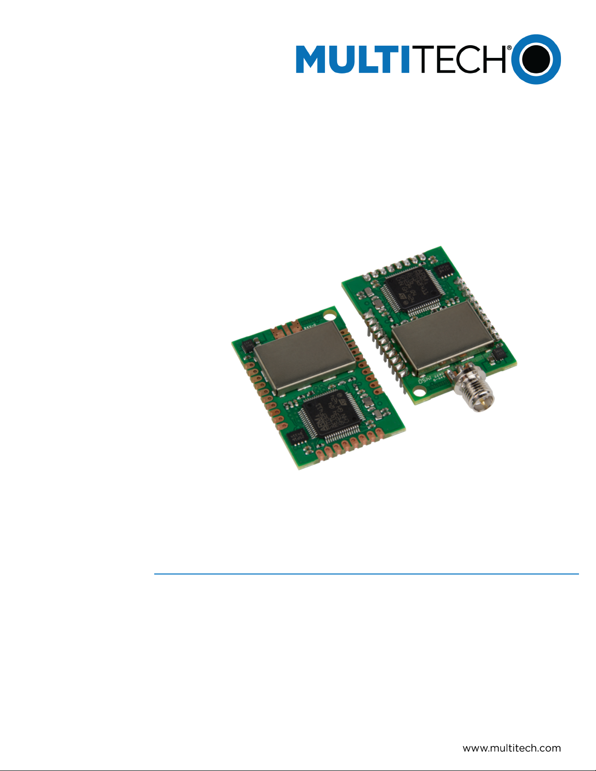
Models: MTDOT-915-xxx, MTDOT-868-xxx includes also the MTUDK2-ST-MDOT Developer Kit
Part Number: S000612, Version 1.5
Copyright
This publication may not be reproduced, in whole or in part, without the specific and express prior written permission signed by an executive officer of
Multi-Tech Systems, Inc. All rights reserved. Copyright © 2015 by Multi-Tech Systems, Inc.
Multi-Tech Systems, Inc. makes no representations or warranties, whether express, implied or by estoppels, with respect to the content, information,
material and recommendations herein and specifically disclaims any implied warranties of merchantability, fitness for any particular purpose and noninfringement.
Multi-Tech Systems, Inc. reserves the right to revise this publication and to make changes from time to time in the content hereof without obligation of
Multi-Tech Systems, Inc. to notify any person or organization of such revisions or changes.
Trademarks and Registered Trademarks
MultiTech, and the MultiTech logo, and MultiConnect are registered trademarks and mDot and Conduit are a trademark of Multi-Tech Systems, Inc. All
other products and technologies are the trademarks or registered trademarks of their respective holders.
Legal Notices
The MultiTech products are not designed, manufactured or intended for use, and should not be used, or sold or re-sold for use, in connection with
applications requiring fail-safe performance or in applications where the failure of the products would reasonably be expected to result in personal injury or
death, significant property damage, or serious physical or environmental damage. Examples of such use include life support machines or other life
preserving medical devices or systems, air traffic control or aircraft navigation or communications systems, control equipment for nuclear facilities, or
missile, nuclear, biological or chemical weapons or other military applications (“Restricted Applications”). Use of the products in such Restricted
Applications is at the user’s sole risk and liability.
MULTITECH DOES NOT WARRANT THAT THE TRANSMISSION OF DATA BY A PRODUCT OVER A CELLULAR COMMUNICATIONS NETWORK WILL BE
UNINTERRUPTED, TIMELY, SECURE OR ERROR FREE, NOR DOES MULTITECH WARRANT ANY CONNECTION OR ACCESSIBILITY TO ANY CELLULAR
COMMUNICATIONS NETWORK. MULTITECH WILL HAVE NO LIABILITY FOR ANY LOSSES, DAMAGES, OBLIGATIONS, PENALTIES, DEFICIENCIES, LIABILITIES,
COSTS OR EXPENSES (INCLUDING WITHOUT LIMITATION REASONABLE ATTORNEYS FEES) RELATED TO TEMPORARY INABILITY TO ACCESS A CELLULAR
COMMUNICATIONS NETWORK USING THE PRODUCTS.
The MultiTech products and the final application of the MultiTech products should be thoroughly tested to ensure the functionality of the MultiTech
products as used in the final application. The designer, manufacturer and reseller has the sole responsibility of ensuring that any end user product into
which the MultiTech product is integrated operates as intended and meets its requirements or the requirements of its direct or indirect customers.
MultiTech has no responsibility whatsoever for the integration, configuration, testing, validation, verification, installation, upgrade, support or maintenance
of such end user product, or for any liabilities, damages, costs or expenses associated therewith, except to the extent agreed upon in a signed written
document. To the extent MultiTech provides any comments or suggested changes related to the application of its products, such comments or suggested
changes is performed only as a courtesy and without any representation or warranty whatsoever.
Contacting MultiTech
Knowledge Base
The Knowledge Base provides immediate access to support information and resolutions for all MultiTech products. Visit http://www.multitech.com/kb.go.
Support Portal
To create an account and submit a support case directly to our technical support team, visit: https://support.multitech.com.
Support
Business Hours: M-F, 8am to 5pm CT
Country By Email By Phone
Europe, Middle East, Africa: support@multitech.co.uk +(44) 118 959 7774
U.S., Canada, all others: support@multitech.com (800) 972-2439 or (763) 717-5863
Warranty
To read the warranty statement for your product, visit www.multitech.com/warranty.go. For other warranty options, visit www.multitech.com/es.go.
World Headquarters
Multi-Tech Systems, Inc.
2205 Woodale Drive, Mounds View, MN 55112
Phone: (800) 328-9717 or (763) 785-3500
Fax (763) 785-9874
2 MultiConnect®mDotTMMTDOT Developer Guide
Page 3

CONTENTS
Contents
Chapter 1 Product Overview .................................................................................................................................... 6
Overview ....................................................................................................................................................................... 6
Getting Started.............................................................................................................................................................. 6
Documentation Overview ............................................................................................................................................. 7
Related Documentation .............................................................................................................................................. 7
mbed Documentation ................................................................................................................................................... 7
Programming the mDot Microcontroller .................................................................................................................... 7
General mBed Links .................................................................................................................................................... 8
mDot Platform ........................................................................................................................................................... 8
EUI and Networking ..................................................................................................................................................... 8
Product Build Options ................................................................................................................................................... 9
Chapter 2 Mechanical Drawings with Pinouts ........................................................................................................ 10
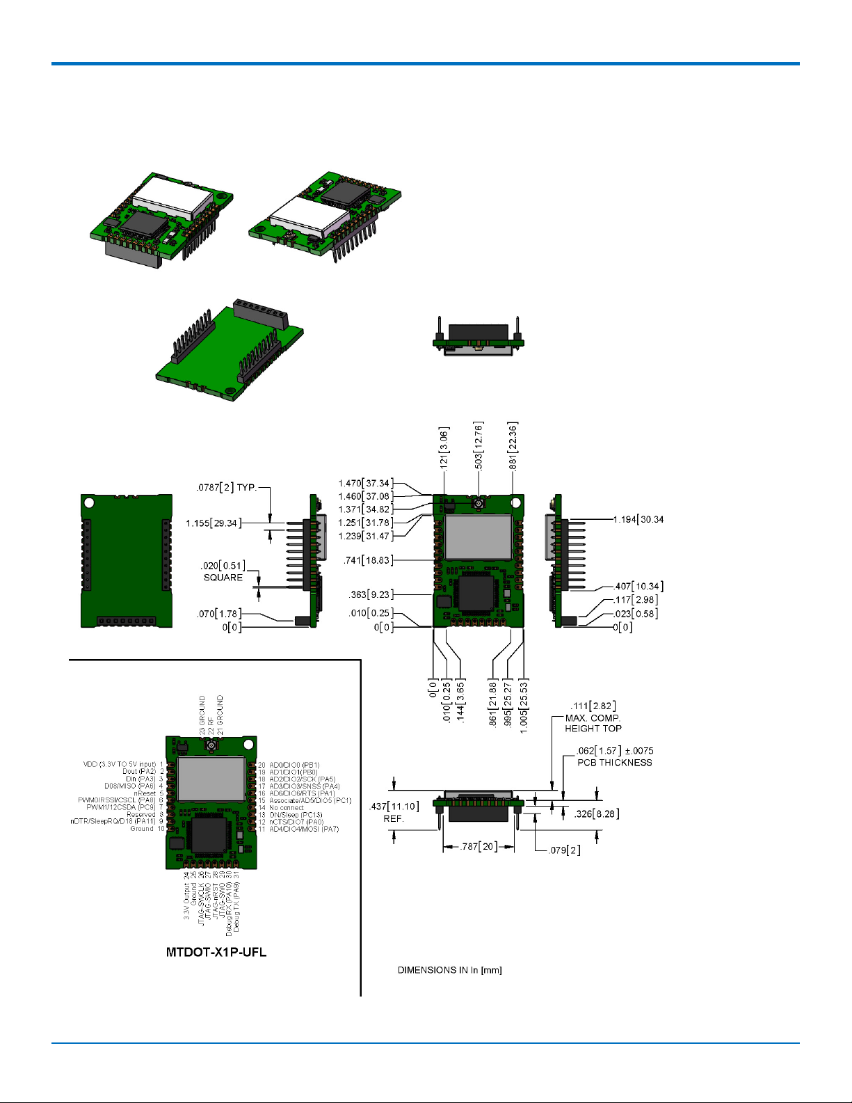
MTDOT-xxx-X1P-SMA.................................................................................................................................................. 10
MTDOT-xxx-X1P-U.FL .................................................................................................................................................. 11
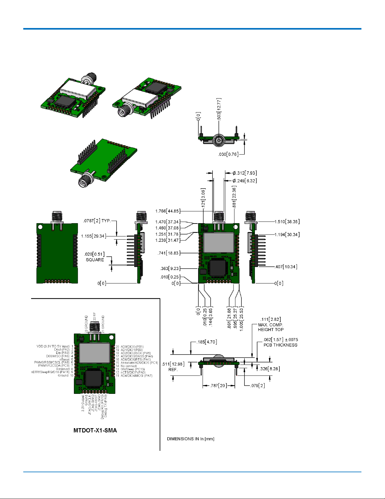
MTDOT-xxx-X1-SMA.................................................................................................................................................... 12
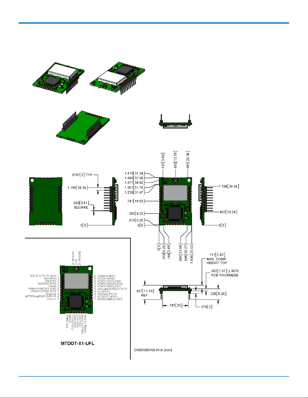
MTDOT-xxx-X1-UFL ..................................................................................................................................................... 13
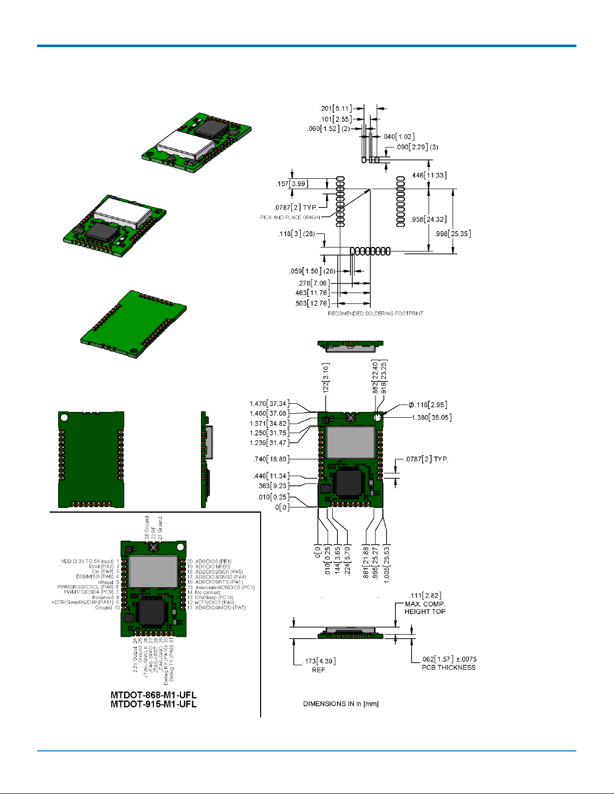
MTDOT-xxx-M1-UFL.................................................................................................................................................... 14
MTDOT-xxx-M1-TRC.................................................................................................................................................... 15
Chapter 3 Specifications and Pin Information ........................................................................................................ 16
MTDOT Specifications ................................................................................................................................................. 16
Power Draw................................................................................................................................................................. 19
Electrical Characteristics ............................................................................................................................................. 20
Pin Information .......................................................................................................................................................... 20
mDot Pinout Design Notes.......................................................................................................................................... 22
Serial Pinout Notes.................................................................................................................................................... 22
Serial Settings.............................................................................................................................................................. 22
LoRa ............................................................................................................................................................................ 22
Throughput Rates...................................................................................................................................................... 22
Range ........................................................................................................................................................................ 23
Chapter 4 Antennas ............................................................................................................................................... 24
Antenna System ......................................................................................................................................................... 24
Pulse Electronics Antenna........................................................................................................................................... 24
Antenna Specifications ............................................................................................................................................. 24
OEM Integration ......................................................................................................................................................... 24
FCC & IC Information to Consumers ......................................................................................................................... 24
FCC Grant Notes........................................................................................................................................................ 25
Host Labeling............................................................................................................................................................. 25
MultiConnect®mDotTMMTDOT Developer Guide 3
Page 4

CONTENTS
Chapter 5 Safety Information................................................................................................................................. 26
Handling Precautions .................................................................................................................................................. 26
Radio Frequency (RF) Safety ....................................................................................................................................... 26
Sécurité relative aux appareils à radiofréquence (RF).............................................................................................. 26
Interference with Pacemakers and Other Medical Devices ...................................................................................... 27
Potential interference............................................................................................................................................... 27
Precautions for pacemaker wearers ........................................................................................................................ 27
Device Maintenance ................................................................................................................................................... 27
User Responsibility...................................................................................................................................................... 27
Chapter 6 Regulatory Information ......................................................................................................................... 28
EMC, Safety, and R&TTE Directive Compliance ......................................................................................................... 28
47 CFR Part 15 Regulation Class B Devices ................................................................................................................. 28
FCC Interference Notice ............................................................................................................................................. 28
FCC Grant .................................................................................................................................................................... 29
FCC Part 15................................................................................................................................................................ 29
FCC Notice................................................................................................................................................................... 29
Industry Canada Class B Notice................................................................................................................................... 29
Industry Canada ......................................................................................................................................................... 30
Chapter 7 Environmental Notices........................................................................................................................... 31
Waste Electrical and Electronic Equipment Statement .............................................................................................. 31
WEEE Directive.......................................................................................................................................................... 31
Instructions for Disposal of WEEE by Users in the European Union ........................................................................ 31
REACH Statement ....................................................................................................................................................... 32
Registration of Substances........................................................................................................................................ 32
Substances of Very High Concern (SVHC) ................................................................................................................ 32
Restriction of the Use of Hazardous Substances (RoHS) ............................................................................................ 33
Information on HS/TS Substances According to Chinese Standards ......................................................................... 34
Information on HS/TS Substances According to Chinese Standards (in Chinese) ...................................................... 35
Chapter 8 Labels .................................................................................................................................................... 36
Approvals and Certification......................................................................................................................................... 36
Example Labels............................................................................................................................................................ 36
Chapter 9 Developer Kit Overview ......................................................................................................................... 37
Developer Board Overview ......................................................................................................................................... 37
Developer Board Features ........................................................................................................................................ 37
MTUDK2-ST-MDOT Developer Kit Contents .............................................................................................................. 37
MTUDK2-ST-CELL Developer Kit Contents ................................................................................................................. 37
Chapter 10 Board Components .............................................................................................................................. 39
Developer Board ........................................................................................................................................................ 39
Developer Board Connectors ...................................................................................................................................... 41
Board Components ..................................................................................................................................................... 41
4 MultiConnect®mDotTMMTDOT Developer Guide
Page 5

CONTENTS
LED Indicators ............................................................................................................................................................. 42
Chapter 11 Developer Board Installation ............................................................................................................... 43
Installing an mDot on the Developer Board ............................................................................................................... 43
Arduino Shield............................................................................................................................................................. 44
mDot Arduino Pins .................................................................................................................................................... 44
Installing an Arduino Shield with an mDot ............................................................................................................... 44
RSMA to U.FL Cables ................................................................................................................................................... 45
Connecting an Antenna through the Developer Board Connectors ........................................................................... 45
Chapter 12 Developer Board Schematics................................................................................................................ 46
Block Diagram ............................................................................................................................................................. 46
Schematics .................................................................................................................................................................. 47
Chapter 13 Design Considerations.......................................................................................................................... 52
Noise Suppression Design ........................................................................................................................................... 52
PC Board Layout Guideline ......................................................................................................................................... 52
User Accessible Areas ............................................................................................................................................... 52
Electromagnetic Interference .................................................................................................................................... 53
Electrostatic Discharge Control................................................................................................................................... 53
USB Design ................................................................................................................................................................. 54
Chapter 14 AT Commands...................................................................................................................................... 55
MultiTech AT Command Set ....................................................................................................................................... 55
General Commands................................................................................................................................................... 55
Network/Addressing Commands .............................................................................................................................. 55
Radio Configuration .................................................................................................................................................. 56
Send/Receive ............................................................................................................................................................ 57
Sleep/Serial Data Mode Options............................................................................................................................... 57
Index...................................................................................................................................................................... 59
MultiConnect®mDotTMMTDOT Developer Guide 5
Page 6
CHAPTER 1 PRODUCT OVERVIEW
Chapter 1 Product Overview
Overview
The MultiConnect mDot is a programmable, long-range RF module that provides encrypted data connectivity to
sensors, industrial equipment, and remote appliances. By using LoRa™Long Range Spread Spectrum technology, bidirectional data communication can be maintained for distances up to 5 miles/8 km line of sight, deep into
buildings, or within noisy environments*using the unlicensed ISM bands in North America, Europe and worldwide.
mDot simplifies local connectivity for Internet of Things (IoT) applications.
The mDot features an integrated ARM®Cortex®-M4 processor and mbedTMcompatible software library for
developers to control, monitor and bring edge intelligence to their Internet of Things (IoT) applications.
*
Actual distance depends on conditions, configuration, antennas, desired throughput, and usage frequency. In
dense urban environments, a typical range is 1-2 miles.
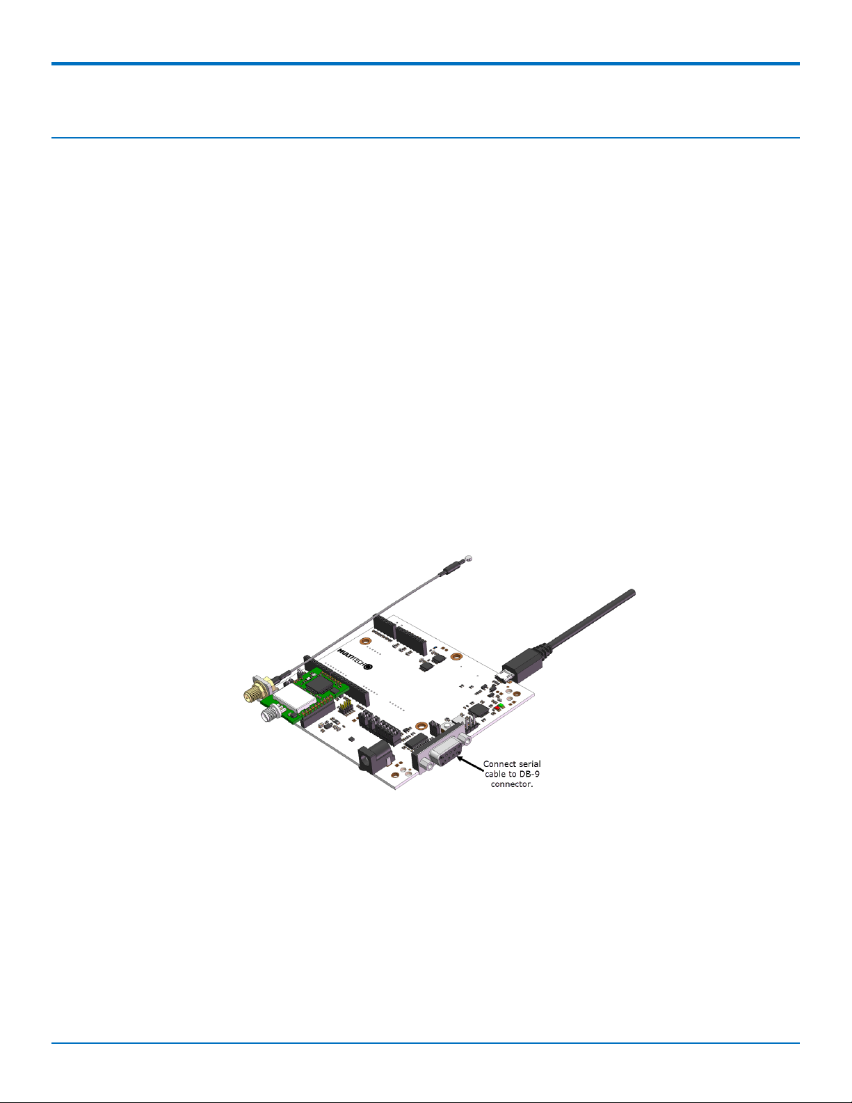
Getting Started
Getting started depends on what you want to do. By default, mDot ships with firmware that supports AT
Commands that use the serial I/O. Refer to Chapter 14, AT Commands.
To send commands to the mDot:
1. Mount the mDot on the developer board. For details, refer to Chapter 11, Developer Board Installation.
2. Connect a serial cable into the DB-9 connector.
3. Open communications software, such as HyperTerminal or TeraTerm.
4. Set the following:
■ Baud rate = 115,200
■ Data bits = 8
■ Parity = N
■ Stop bits = 1
■ Flow control = Off
6 MultiConnect®mDotTMMTDOT Developer Guide
Page 7

CHAPTER 1 PRODUCT OVERVIEW
Two serial interfaces are available through the USB interface, one is used to program the mDot and the other is for
debug messages. Refer to “mDot Pinout Design Notes” in Chapter 3, Specifications and Pin Information for
information on which pins are available out of the box.
To develop using mbed, the mDot mbed page includes libraries and test cases. Refer to “mBed Documentation” for
details and links.
For help setting up a MultiConnect®Conduit™to send data to and from an mDot, refer to “Related
Documentation.”
Documentation Overview
This manual is one part of mDot documentation. Refer to the Related Documentation and mbed sections for
additional information needed to program your mDot and integrate your application with the MultiConnect
Conduit gateway.
This document includes the following sections:
■ mDot device information: Mechanical drawings, specifications, safety and regulatory information, and other
device specific content. Chapters 1-8
■ Universal Developer Kit information: Using the MTUDK-ST-MDOT Developer Kit, including design
considerations, schematics, and installation and operation information. Chapters 9-13
■ AT commands: Includes MultiTech AT Commands. Chapter 14.
This manual is available at www.multitech.com/support.
Related Documentation
Application notes, LoRa information, and documentation for related products such as the MultiConnect Conduit
(MTCDT) gateway and the LoRa accessory card (MTAC-LORA) are available on the MultiTech developer site. This
site includes information on using the Conduit with mDots. Go to: www.multitech.net
For a datasheet and information on the STmicro ARM®Cortex®-M4 processor from go to:
http://www.st.com/web/en/catalog/mmc/FM141/SC1169/SS1577/LN1877/PF260049
mbed Documentation
ARM mbed is a free, open-source platform and operating system for embedded devices using the ARM Coretx-M
microcontrollers. The mbed website provides free software libraries, hardware designs, and online tools for rapid
prototyping of products. The platform includes a standards-based C/C++ SDK, a microcontroller HDK, and
supported development boards, an online compiler and online developer collaboration tools.
Note: To send and receive data, you need a LoRaWAN 1.0 gateway, such as MultTech's MultiConnect Conduit
(MTCDT) with an MTAC-LORA accessory card installed.
Programming the mDot Microcontroller
With the mDot and the MTUDK2-ST-xx developer board, use the ARM mbed ecosystem to program the
microcontroller. Compile in the cloud or locally, copy the resulting binary file to the mbed USB drive, and reset the
mDot.
Note: To program the mDot, you need an mDot model with programming header, model MTDOT-xx-X1P-SMA.
MultiConnect®mDotTMMTDOT Developer Guide 7
Page 8

CHAPTER 1 PRODUCT OVERVIEW
On the mDot mbed page, MultiTech supplies source code for non-RF portions of the mDot and MTAC-LORA cards.
To comply with FCC and ETSI certification, some portions of the software will be available only as binary libraries.
General mBed Links
■ Explore mbed: http://developer.mbed.org/explore
■ Getting Started with mbed: http://developer.mbed.org/getting-started
■ mbed Handbook: http://developer.mbed.org/handbook/Homepage
mDot Platform
The mDot mbed page includes the mDot library, firmware, and test cases
https://developer.mbed.org/platforms/MTS-mDot-F411
EUI and Networking
All mDots have a factory-programmed Extended Unique Identifier (EUI). This is marked as Node on the mDot label.
To connect an mDot to a network, you will need to program it with the network ID for the network you are
connecting to as well as the network key and application key. For information on setting up mDots as part of a
LoRa network, go to: www.multitech.net
8 MultiConnect®mDotTMMTDOT Developer Guide
Page 9
CHAPTER 1 PRODUCT OVERVIEW
Product Build Options
Product Description Quanity to Order
North America
MTDOT-915-X1-SMA 915 MHz XBee LoRa SMA 1 or 50
MTDOT-915-X1P-SMA 915 MHz XBee LoRa SMA with Programming Header 1
MTDOT-915-X1-UFL 915 MHz XBee LoRa U.FL 1 or 50
MTDOT-915-M1-UFL 915 MHz SMT LoRa U.FL 1 or 100
MTDOT-915-M1-TRC 915 MHz SMT LoRa RF Pad 1 or 100
EMEA
MTDOT-868-X1-SMA 868 MHz XBee LoRa SMA 1 or 50
MTDOT-868-X1P-SMA 868 MHz XBee LoRa SMA with Programming Header 1
MTDOT-868-X1-UFL 868 MHz XBee LoRa U.FL 1 or 50
MTDOT-868-M1-UFL 868 MHz SMT LoRa U.FL 1 or 100
MTDOT-868-M1-TRC 868 MHz SMT LoRa RF Pad 1 or 100
Developer Kits
MTUDK2-ST-MDOT mDot Developer Kit 1
Note:
■ The complete product code may end in .Rx. For example, MTDOT-915-M1-X1.Rx, where R is revision
and x is the revision number.
MultiConnect®mDotTMMTDOT Developer Guide 9
Page 10

CHAPTER 2 MECHANICAL DRAWINGS WITH PINOUTS
Chapter 2 Mechanical Drawings with Pinouts
MTDOT-xxx-X1P-SMA
10 MultiConnect®mDotTMMTDOT Developer Guide
Page 11
MTDOT-xxx-X1P-U.FL
CHAPTER 2 MECHANICAL DRAWINGS WITH PINOUTS
MultiConnect®mDotTMMTDOT Developer Guide 11
Page 12
CHAPTER 2 MECHANICAL DRAWINGS WITH PINOUTS
MTDOT-xxx-X1-SMA
12 MultiConnect®mDotTMMTDOT Developer Guide
Page 13
MTDOT-xxx-X1-UFL
CHAPTER 2 MECHANICAL DRAWINGS WITH PINOUTS
MultiConnect®mDotTMMTDOT Developer Guide 13
Page 14
CHAPTER 2 MECHANICAL DRAWINGS WITH PINOUTS
MTDOT-xxx-M1-UFL
14 MultiConnect®mDotTMMTDOT Developer Guide
Page 15
MTDOT-xxx-M1-TRC
CHAPTER 2 MECHANICAL DRAWINGS WITH PINOUTS
MultiConnect®mDotTMMTDOT Developer Guide 15
Page 16
CHAPTER 3 SPECIFICATIONS AND PIN INFORMATION
Chapter 3 Specifications and Pin Information
MTDOT Specifications
Category Description
General
Compatibility LoRaWAN 1.0 specifications
Interfaces Note that pin functions are multiplexed.
Up to 16 digital I/O
Up to 11 analog inputs
SPI
I2C
UART (RX, TX, RTS, CTS)
USB (OTG full speed)
CPU Performance
CPU STM32
Max Clock 100 MHz (configurable to control power use)
Flash Memory 512 KB (400 KB available)
RAM 128 KB
Radio Frequency
ISM Bands 863 MHz - 868 MHz, 902 MHz - 928 MHz
Physical Description
Weight
Dimensions Refer to Mechanical Drawings for Dimensions.
RF Connectors
-SMA Models SMA
-UFL Models U.FL
-Trace Models Trace Connection
Environment
Operating Temperature -40° C to +85° C
1
0.2 oz. (5g)
Storage Temperature -40° C to +85° C
Humidity 20%-90% RH, non-condensing
Power Requirements
Operating Voltage 3.3 V
16 MultiConnect®mDotTMMTDOT Developer Guide
Page 17
Category Description
Certifications and Compliance
EMC Compliance EN 300 220-2 V2.4.1:2012
EN 301 489-03 V1.6.1:2013
Radio Compliance FCC 15.247:2015
FCC 15.109:2015
FCC 15.107:2015
RSS-210:2010
ICES-003:2012
CISPR 22:2008
EN 300 220-2 V2.4.1:2012
Safety Compliance UL 60950-1 2nd ED
cUL 60950-1 2nd ED
CHAPTER 3 SPECIFICATIONS AND PIN INFORMATION
IEC 60950-1 2nd ED AM1 + AM2
1
Weight is for the MTDOT-xxx-X1P-SMA, which is the heaviest model.
Category Description
Transmission
2
North America EMEA
Max Transmitter 15 dBm 14 dBm
Power Output (TPO)
Maximum Receive -137 dBm -137 dBm
Sensitivity
Link Budget
3
147 dB Point-to-Point 147 dB Point-to-Point
Max Effective 22 dBm 10 dBm
Isotropic Radiated
Power (EiRP)
Receive Sensitivity
Spreading Factor North America Typical Sensitivity
4
EMEA Typical Sensitivity
6 -111 dBm -121 dBm
5
7 -116 dBm -124 dBm
8 -119 dBm -127 dBm
9 -122 dBm -130 dBm
10 -125 dBm -133 dBm
11 Not Applicable -135 dBm
12 Not Applicable -137 dBm
MultiConnect®mDotTMMTDOT Developer Guide 17
Page 18

CHAPTER 3 SPECIFICATIONS AND PIN INFORMATION
2
Using the Pulse Electronics W1063 antenna, described in the Chapter 4, Antennas.
3
Greater link budget is possible with higher gain antenna.
4
RFS_L500: RF sensitivity, Long-Range Mode, highest LNA gain, LNA boost, 500 kHz bandwidth using split Rx/Tx
path.
5
RFS_L125: RF sensitivity, Long-Range Mode, highest LNA gain, LNA boost, 125 kHz bandwidth using split Rx/Tx
path.
18 MultiConnect®mDotTMMTDOT Developer Guide
Page 19

CHAPTER 3 SPECIFICATIONS AND PIN INFORMATION
Power Draw
Note:
■ Sleep command is supported on firmware Version 0.1.2 and newer.
■ Transmit power measured with MTDOT-915-xx transmitting to a MultiConnect Conduit with an
MTAC-LORA-915 accessory card installed.
■ mDot was Revision B PCB with firmware Version 0.0.14.
■ Idle current measured with the mDot joined with Conduit, but idle without data transferring.
■ Transmit power measured while transferring data packets using spread factor 9. Packet size limited
to 53 bytes. The Conduit was set to receive packets from and send back to the mDot. A script was
run to send the packet 100 times with either 10 or 53 bytes of data, with an average measurement
taken during that time.
■ For Inrush charge took five separate measurements and recorded the highest observed value.
■ Power measurements are similar for 868 MHz models. Some 868 MHz sub-band frequencies do not
support maximum TXP power of 20.
Voltage Sleep Idle current Packet Size Average Average Average Total Total
Mode Average (Bytes) Current Current Current Inrush Inrush
(Available (Amps) (Amps) at (Amps) at (Amps) at Charge Charge
on Low Default Maximum Measured Duration
Version Transmit Transmit Transmit in during
0.1.2 or Power Power Power Millicoulo Powerup
newer) Setting Setting Setting mbs (mC) (InRush
(TXP 2) (TXP 11) (TXP 20) Duration)
3.3 Standby 0.032 10 0.026 0.028 0.031 1.14 661uS
Mode
30.9uA
5.0 Standby 0.032 10 0.026 0.028 0.032 1.79 1.24mS
Mode
33.5uA
0.032 53 0.026 0.029 0.041 1.14 661uS
0.032 53 0.025 0.028 0.042 1.79 1.24mS
MultiConnect®mDotTMMTDOT Developer Guide 19
Page 20

CHAPTER 3 SPECIFICATIONS AND PIN INFORMATION
Electrical Characteristics
Signal Description Min Max
Vin Low Input low level -- .99
Vin High Input high level 2.31 --
Vout Low Output low level -- .4
Vout High Output high level 2.9 --
VCC Standard operating voltage 3.3 5
ICC Operating current (mA) -- 135
@5V
Operating current (mA) -- 200
@3.3V
Pin Information
Using the mbed platform with the Cortex-M4 processor expands your pin functionality options. Refer to the
document, mDot Pin Function Mapping, which is available at www.multitech.net/developer/multiconnect-mdot
and https://developer.mbed.org/platforms/MTS-mdot-f411/ for details.
MT Pin Base Number (Where applicable) Description
1 VDD (3.3 to 5 V input)
2 PA2 PA_2/XBEE_Dout
3 PA3 PA_3/XBEE_Din
4 PA6 PA_6/XBEE_D08/SPI1_MISO
5 nReset
6 PA8 PA_8/XBEE_PWM0/XBEE_RSSI/I2C_S
CL
7 PA9 PA_9/XBEE_PWM1/I2C_SDA
8 Reserved
9 PA11 PA_11/XBEE_nDTR/XBEE_SleepRQ/X
BEE_D18
10 Ground
11 PA7 PA_7/XBEE_AD4/XBEE_DIO4/SPI1_M
OSI
12 PA0 PA_0/XBEE_nCTS/XBEE_DIO7/LED1
13 PC13 PC_13/XBEE_ON_Sleep
14 No connect
15 PC1 PC_1/XBEE_Associate/XBEE_AD5/XB
EE_DIO5
20 MultiConnect®mDotTMMTDOT Developer Guide
Page 21

CHAPTER 3 SPECIFICATIONS AND PIN INFORMATION
MT Pin Base Number (Where applicable) Description
16 PA1 PA_1/XBEE_AD6/XBEE_DIO6/XBEE_R
TS
17 PA4 PA_4/XBEE_AD3/XBEE_DIO3/SPI1_C
S
18 PA5 PA_5/XBEE_AD2/XBEE_DIO2/SPI1_S
CK
19 PB0 PB_0/XBEE_AD1/XBEE_DIO1
20 PB1 PB_1/XBEE_AD0/XBEE_DIO0
21 Ground
22 RF
23 Ground
24 VOUT (3.3V output)
25 Ground
26 PA14 PA_14/JTAG-SWCLK
27 PA13 PA_13/JTAG-SWIO
28 PB4 PB_4/JTAG-nRST
29 PB3 PB_3/JTAG-SWO
30 PA10 PA_10/Debug RX/
31 PA9 PA_9/Debug TX/USBTX
MultiConnect®mDotTMMTDOT Developer Guide 21
Page 22

CHAPTER 3 SPECIFICATIONS AND PIN INFORMATION
mDot Pinout Design Notes
Refer to the mechanical drawing for your model for pin locations.
■ All pins that go to connectors are directly connected to the processor.
■ Reset is the only pin with pull up.
■ I/O is 5V tolerant.
mDots allow you to program pins depending on your application:
■ Serial: Available out of the box. See Serial Pinout Notes for details.
■ Xbee: Comforms to the Xbee pinout.
■ mbed: Designed with the mbed STM32F411 RET 64-pin processor, this option provides the most flexibility.
For more information about processor capabilities, see the STM32F411 RET datasheet.
Note: To program the mDot, you need an mDot model with programming header., model MTDOT-xx-X1P-SMA
Serial Pinout Notes
Out of the box, these pins are available for serial applications. Refer to the mechanical drawing for your model for
pin locations.
■ 2 Dout/TX
■ 3 Din/RX
■ 9 DTR
■ 12 CTS
■ 13 On/Sleep
■ 16 RTS
Serial Settings
When creating a serial connection with an mDot on the developer board, connect a serial cable to the DB-9
connector, open communications software (such as HyperTerminal or TeraTerm), and use the following settings:
■ Baud rate = 115,200
■ Data bits = 8
■ Parity = N
■ Stop bits = 1
■ Flow control = Off
LoRa
Throughput Rates
Theoretical maximum speeds for LoRa mode with ACKs off are:
■ Using spreading factor 7 at 125kHz, the throughput rate is 5470 bps (5.47 kbps).
■ Using spreading factor 7 at 500kHz the receiving throughput rate is 21900 bps (21.9 kbps).
Note: Data rates in the LoRaWAN specification vary by geographic region.
22 MultiConnect®mDotTMMTDOT Developer Guide
Page 23

CHAPTER 3 SPECIFICATIONS AND PIN INFORMATION
Range
Variables effecting the mDot range include TX power, antenna gain, RX sensitivity, fade margin, earth's curvature.
Use the following formula to calculate the maximum range:
The following table provides example settings and the theoretical maximum range based on these settings.
Example 18dB Transmit Power for Units Example 14dB Transmit Power for
915 MHz Models 868MHz Models
Frequency 915 MHz 868
TX Power 18 dBm 14
TX Antenna Gain 3 dB 3
RX Sensitivity
RX Antenna Gain 3 dB 3
Fade Margin
1
2
-120 dBm -120
30 dB 30
Distance 8.14 Miles 5.41
Distance 13.08 Km 8.70
1
RX Sensitivity is set to a conservative -120dBm, but can vary from -117 to -137dBm.
2
Fade Margin is set at the worst case of 30dB. Fade margin is an allowance a system designer includes to account
for unknown variables. The higher the fade margin, the better the overall link quality will be. With a fade margin
set to zero, the link budget is still valid, but only in LOS conditions, which is not practical for most designs. The
amount of fade margin to include in a calculation depends on the environment in which you will deploy the
system. A fade margin of 12 dBm is good, but a better number would be 20 to 30 dBm.
MultiConnect®mDotTMMTDOT Developer Guide 23
Page 24

CHAPTER 4 ANTENNAS
Chapter 4 Antennas
Antenna System
The LoRa antenna performance depends on the implementation and antenna design. The integration of the
antenna system into the product is a critical part of the design process; therefore, it is essential to consider it early
so the performance is not compromised. If changes are made to the device's certified antenna system, then
recertification will be required.
This radio transmitter IC ID 125A-0054, MTDOT-915 has been approved by Industry Canada to operate with the
antenna types listed below with the maximum permissible gain indicated. Antenna types not included in this list,
having a gain greater than the maximum gain indicated for that type, are strictly prohibited for use with this
device.
Pulse Electronics Antenna
Manufacturer: Pulse Electronics
Description: 868-915 MHz RP-SMA Antenna, 8"
Model Number: W1063
MultiTech Part Number: 45009830L
MultiTech ordering information:
Ordering Part Number Quantity
AN868-915A-1HRA 1
AN868-915A-10HRA 10
AN868-915A-50HRA 50
Antenna Specifications
Category Description
Frequency Range 868-928 MHz
Impedance 50 Ohms
VSWR < 2.0
Gain 3.0 dBi
Radiation Omni
Polarization Vertical
OEM Integration
FCC & IC Information to Consumers
The user manual for the consumer must contain the statements required by the following FCC and IC regulations:
47 C.F.R. 15.19(a)(3), 15.21, 15.105 and RSS-Gen Issue 3, Dec 2010; 7.1.2 and 7.1.3
24 MultiConnect®mDotTMMTDOT Developer Guide
Page 25

CHAPTER 4 ANTENNAS
FCC Grant Notes
The OEM should follow all the grant notes listed below. Otherwise, further testing and device approvals may be
necessary.
FCC Definitions
Portable: (§2.1093) — A portable device is defined as a transmitting device designed to be used so that the
radiating structure(s) of the device is/are within 20 centimeters of the body of the user.
Mobile: (§2.1091) — A mobile device is defined as a transmitting device designed to be used in other than fixed
locations and to generally be used in such a way that a separation distance of at least 20 centimeters is normally
maintained between the transmitter’s radiating structure(s) and the body of the user or nearby persons.
Actual content pending Grant: This device is a mobile device with respect to RF exposure compliance. The
antenna(s) used for this transmitter must be installed to provide a separation distance of at least 20 cm from all
persons, and must not be collocated or operate in conjunction with any other antenna or transmitter except in
accordance with FCC multi-transmitter product guidelines. Installers and end-users must be provided with specific
information required to satisfy RF exposure compliance for installations and final host devices. (See note under
Grant Limitations.) Compliance of this device in all final host configurations is the responsibility of the Grantee.
Note: Host design configurations constituting a device for portable use (<20 cm from human body) require
separate FCC/IC approval.
Host Labeling
The following statements are required to be on the host label:
This device contains FCC ID: {Add the FCC ID of the specific device}
This device contains equipment certified under IC ID: {Add the IC ID of the specific device}
For additional labeling requirements, see the product's Labeling Requirements. For the FCC and IC IDs, see specific
certificate information in the Regulatory Statement chapter.
MultiConnect®mDotTMMTDOT Developer Guide 25
Page 26

CHAPTER 5 SAFETY INFORMATION
Chapter 5 Safety Information
Handling Precautions
To avoid damage due to the accumulation of static charge, use proper precautions when handling any cellular
device. Although input protection circuitry has been incorporated into the devices to minimize the effect of static
build-up, use proper precautions to avoid exposure to electronic discharge during handling and mounting the
device.
Radio Frequency (RF) Safety
Due to the possibility of radio frequency (RF) interference, it is important that you follow any special regulations
regarding the use of radio equipment. Follow the safety advice given below.
■ Operating your device close to other electronic equipment may cause interference if the equipment is
inadequately protected. Observe any warning signs and manufacturers’ recommendations.
■ Different industries and businesses restrict the use of cellular devices. Respect restrictions on the use of
radio equipment in fuel depots, chemical plants, or where blasting operations are in process. Follow
restrictions for any environment where you operate the device.
■ Do not place the antenna outdoors.
■ Switch OFF your wireless device when in an aircraft. Using portable electronic devices in an aircraft may
endanger aircraft operation, disrupt the cellular network, and is illegal. Failing to observe this restriction
may lead to suspension or denial of cellular services to the offender, legal action, or both.
■ Switch OFF your wireless device when around gasoline or diesel-fuel pumps and before filling your vehicle
with fuel.
■ Switch OFF your wireless device in hospitals and any other place where medical equipment may be in use.
Sécurité relative aux appareils à radiofréquence (RF)
À cause du risque d'interférences de radiofréquence (RF), il est important de respecter toutes les réglementations
spéciales relatives aux équipements radio. Suivez les conseils de sécurité ci-dessous.
■ Utiliser l'appareil à proximité d'autres équipements électroniques peut causer des interférences si les
équipements ne sont pas bien protégés. Respectez tous les panneaux d'avertissement et les
recommandations du fabricant.
■ Certains secteurs industriels et certaines entreprises limitent l'utilisation des appareils cellulaires. Respectez
ces restrictions relatives aux équipements radio dans les dépôts de carburant, dans les usines de produits
chimiques, ou dans les zones où des dynamitages sont en cours. Suivez les restrictions relatives à chaque
type d'environnement où vous utiliserez l'appareil.
■ Ne placez pas l'antenne en extérieur.
■ Éteignez votre appareil sans fil dans les avions. L'utilisation d'appareils électroniques portables en avion est
illégale: elle peut fortement perturber le fonctionnement de l'appareil et désactiver le réseau cellulaire. S'il
ne respecte pas cette consigne, le responsable peut voir son accès aux services cellulaires suspendu ou
interdit, peut être poursuivi en justice, ou les deux.
■ Éteignez votre appareil sans fil à proximité des pompes à essence ou de diesel avant de remplir le réservoir
de votre véhicule de carburant.
26 MultiConnect®mDotTMMTDOT Developer Guide
Page 27

CHAPTER 5 SAFETY INFORMATION
■ Éteignez votre appareil sans fil dans les hôpitaux ou dans toutes les zones où des appareils médicaux sont
susceptibles d'être utilisés.
Interference with Pacemakers and Other Medical Devices
Potential interference
Radiofrequency energy (RF) from cellular devices can interact with some electronic devices. This is electromagnetic
interference (EMI). The FDA helped develop a detailed test method to measure EMI of implanted cardiac
pacemakers and defibrillators from cellular devices. This test method is part of the Association for the
Advancement of Medical Instrumentation (AAMI) standard. This standard allows manufacturers to ensure that
cardiac pacemakers and defibrillators are safe from cellular device EMI.
The FDA continues to monitor cellular devices for interactions with other medical devices. If harmful interference
occurs, the FDA will assess the interference and work to resolve the problem.
Precautions for pacemaker wearers
If EMI occurs, it could affect a pacemaker in one of three ways:
■ Stop the pacemaker from delivering the stimulating pulses that regulate the heart's rhythm.
■ Cause the pacemaker to deliver the pulses irregularly.
■ Cause the pacemaker to ignore the heart's own rhythm and deliver pulses at a fixed rate.
Based on current research, cellular devices do not pose a significant health problem for most pacemaker wearers.
However, people with pacemakers may want to take simple precautions to be sure that their device doesn't cause
a problem.
■ Keep the device on the opposite the side of the body from the pacemaker to add extra distance
between the pacemaker and the device.
■ Avoid placing a turned-on device next to the pacemaker (for example, don’t carry the device in a shirt
or jacket pocket directly over the pacemaker).
Device Maintenance
When maintaining your device:
■ Do not attempt to disassemble the device. There are no user serviceable parts inside.
■ Do not expose your device to any extreme environment where the temperature or humidity is high.
■ Do not expose the device to water, rain, or spilled beverages. It is not waterproof.
■ Do not place the device alongside computer discs, credit or travel cards, or other magnetic media. The
information contained on discs or cards may be affected by the device.
■ Using accessories, such as antennas, that MultiTech has not authorized or that are not compliant with
MultiTech's accessory specifications may invalidate the warranty.
If the device is not working properly, contact MultiTech Technical Support.
User Responsibility
Respect all local regulations for operating your wireless device. Use the security features to block unauthorized use
and theft.
MultiConnect®mDotTMMTDOT Developer Guide 27
Page 28

CHAPTER 6 REGULATORY INFORMATION
Chapter 6 Regulatory Information
EMC, Safety, and R&TTE Directive Compliance
The CE mark is affixed to this product to confirm compliance with the following European Community Directives:
Council Directive 2004/108/EC of 15 December 2004 on the approximation of the laws of Member States
relating to electromagnetic compatibility;
and
Council Directive 2006/95/EC of 12 December 2006 on the harmonization of the laws of Member States
relating to electrical equipment designed for use within certain voltage limits;
and
Council Directive 2011/65/EU on the restriction of the use of certain hazardous substances in electrical
and electronic equipment;
and
Council Directive 1999/5/EC of 9 March 1999 on radio equipment and telecommunications terminal
equipment and the mutual recognition of their conformity.
47 CFR Part 15 Regulation Class B Devices
This equipment has been tested and found to comply with the limits for a Class B digital device, pursuant to part
15 of the FCC Rules. These limits are designed to provide reasonable protection against harmful interference in a
residential installation. This equipment generates, uses, and can radiate radio frequency energy and, if not installed
and used in accordance with the instructions, may cause harmful interference to radio communications. However,
there is no guarantee that interference will not occur in a particular installation. If this equipment does cause
harmful interference to radio or television reception, which can be determined by turning the equipment off and
on, the user is encouraged to try to correct the interference by one or more of the following measures:
■ Reorient or relocate the receiving antenna.
■ Increase the separation between the equipment and receiver.
■ Connect the equipment into an outlet on a circuit different from that to which the receiver is connected.
■ Consult the dealer or an experienced radio/TV technician for help.
Warning: Changes or modifications to this unit not expressly approved by the party responsible for compliance
could void the user’s authority to operate the equipment.
FCC Interference Notice
Per FCC 15.19(a)(3) and (a)(4) This device complies with part 15 of the FCC Rules. Operation is subject to the
following two conditions: (1) This device may not cause harmful interference, and (2) this device must accept any
interference received, including interference that may cause undesired operation.
28 MultiConnect®mDotTMMTDOT Developer Guide
Page 29

CHAPTER 6 REGULATORY INFORMATION
FCC Grant
FCC Part 15
FCC Identifier: AU792U13A16857
Equipment Class: Digital Transmission System
Notes: MTDOT-915
FCC Rule Parts: 15C
Approval: Single Modular
Frequency Range: 902.3-914.9
Output Watts: 0.0772
Output power is conducted. This transmitter is a hybrid per FCC 15.247(f) and FCC KDB 453039. The antenna(s)
used for this transmitter must be installed to provide a separation distance of at least 20 cm from all persons and
must not be collocated or operating in conjunction with any other antenna or transmitter within a host device,
except in accordance with FCC multi-transmitter product procedures. End-users and installers must be provided
with antenna installation instructions and transmitter operating conditions for satisfying RF exposure compliance.
FCC Notice
The MTDOT-x family of products are open development based products that contain a sub ghz radio technology.
MultiTech has certified for compliance with US and Foreign compliance bodies including FCC, R&TTE and others.
(e.g. FCC 15.247:2015 & IC RSS-210:2010)
MultiTech provides software code meant to operate the radio to a level that maintains compliance with the
operating modes under which these radio devices were certified. To ensure this level of compliance, the software
code is provided in binary form only. Users are prohibited from making any changes that affect the operation of
the radio performance. Accessing or controlling the radio through any means other than the provided binary
software will require the user to obtain their own intentional radiator license from the certification body governing
their locality, as all precertification provided with mDot will have been made invalid.
Industry Canada Class B Notice
This Class B digital apparatus meets all requirements of the Canadian Interference-Causing Equipment Regulations.
Cet appareil numérique de la classe B respecte toutes les exigences du Reglement Canadien sur le matériel
brouilleur.
This device complies with Industry Canada RSS Appliance radio exempt from licensing. The operation is permitted
for the following two conditions:
1. the device may not cause harmful interference, and
2. the user of the device must accept any interference suffered, even if the interference is likely to
jeopardize the operation.
Le présent appareil est conforme aux CNR d'Industrie Canada applicables aux appareils radio exempts de licence.
L'exploitation est autorisée aux deux conditions suivantes:
1. l'appareil ne doit pas produire de brouillage, et
MultiConnect®mDotTMMTDOT Developer Guide 29
Page 30

CHAPTER 6 REGULATORY INFORMATION
2. l'utilisateur de l'appareil doit accepter tout brouillage radioélectrique subi, même si le brouillage est
susceptible d'en compromettre le fonctionnement.
Industry Canada
Certification Number/No. de Certification
Type of Radio Equipment/Genre de Matériel Spread Spectrum/Digital Device (902-928MHz)/
Model/Modèle MTDOT-915
Specification/Ca Issue/Édit From To Emmission Minimu Maximum Power
hier des Charges ion Frequency/D Frequency Designation/Desig m
e Fréquences /Á nation D’émission Power
Fréquence
s
RSS247 1.0 902.3 MHz 914.9 MHz GXDXX 77.2 77.2 mW
Certification of equipment means only that the equipment has met the requirements of the above noted
specification. License applications, where applicable to use certified equipment, are acted on accordingly by the
Industry Canada issuing office and will depend on the existing radio environment, service and location of
operation. This certificate is issued on condition that the holder complies and will continue to comply with the
requirements and procedures issued by Industry Canada. The equipment for which this certificate is issued shall
not be manufactured, imported distributed, leased, offered for sale or sold unless the equipment complies with
the applicable technical specifications and procedures issued by Industry Canada.
125A-0054
Modular Approval/Approbation modulaire
mW
La certification du matériel signifie seulement que le matériel a satisfait aux exigences de la norme indiquée cidessus. Les demandes de licences nécessaires pour l’utilisation du matériel certifié sont traitées en conséquence
par le bureau de délivrance d’Industrie Canada et dépendent des conditions radio ambiantes, du service et de
l’emplacement d’exploitation. Le présent certificat est délivré à la condition que le titulaire satisfasse et continue
de satisfaire aux exigences et aux procédures d’Industrie Canada. Le matériel à l’égard duquel le présent certificat
est délivré ne doit pas être fabriqué, importé, distribué, loué, mis en vente ou vendu à moins d’être conforme aux
procédures et aux spécifications techniques applicable publiées par Industrie Canada.
30 MultiConnect®mDotTMMTDOT Developer Guide
Page 31

CHAPTER 7 ENVIRONMENTAL NOTICES
Chapter 7 Environmental Notices
Waste Electrical and Electronic Equipment Statement
Note: This statement may be used in documentation for your final product applications.
WEEE Directive
The WEEE Directive places an obligation on EU-based manufacturers, distributors, retailers, and importers to takeback electronics products at the end of their useful life. A sister directive, ROHS (Restriction of Hazardous
Substances) complements the WEEE Directive by banning the presence of specific hazardous substances in the
products at the design phase. The WEEE Directive covers all MultiTech products imported into the EU as of August
13, 2005. EU-based manufacturers, distributors, retailers and importers are obliged to finance the costs of recovery
from municipal collection points, reuse, and recycling of specified percentages per the WEEE requirements.
Instructions for Disposal of WEEE by Users in the European Union
The symbol shown below is on the product or on its packaging, which indicates that this product must not be
disposed of with other waste. Instead, it is the user's responsibility to dispose of their waste equipment by handing
it over to a designated collection point for the recycling of waste electrical and electronic equipment. The separate
collection and recycling of your waste equipment at the time of disposal will help to conserve natural resources
and ensure that it is recycled in a manner that protects human health and the environment. For more information
about where you can drop off your waste equipment for recycling, please contact your local city office, your
household waste disposal service or where you purchased the product.
July, 2005
MultiConnect®mDotTMMTDOT Developer Guide 31
Page 32

CHAPTER 7 ENVIRONMENTAL NOTICES
REACH Statement
Registration of Substances
After careful review of the legislation and specifically the definition of an “article” as defined in EC Regulation
1907/2006, Title II, Chapter 1, Article 7.1(a)(b), it is our current view Multi-Tech Systems, Inc. products would be
considered as “articles”. In light of the definition in § 7.1(b) which requires registration of an article only if it
contains a regulated substance that “is intended to be released under normal or reasonably foreseeable conditions
of use,” Our analysis is that Multi-Tech Systems, Inc. products constitute nonregisterable articles for their intended
and anticipated use.
Substances of Very High Concern (SVHC)
Per the candidate list of Substances of Very High Concern (SVHC) published October 28, 2008 we have reviewed
these substances and certify the Multi-Tech Systems, Inc. products are compliant per the EU “REACH”
requirements of less than 0.1% (w/w) for each substance. If new SVHC candidates are published by the European
Chemicals Agency, and relevant substances have been confirmed, that exceeds greater than 0.1% (w/w), MultiTech Systems, Inc. will provide updated compliance status.
Multi-Tech Systems, Inc. also declares it has been duly diligent in ensuring that the products supplied are compliant
through a formalized process which includes collection and validation of materials declarations and selective
materials analysis where appropriate. This data is controlled as part of a formal quality system and will be made
available upon request.
32 MultiConnect®mDotTMMTDOT Developer Guide
Page 33

CHAPTER 7 ENVIRONMENTAL NOTICES
Restriction of the Use of Hazardous Substances (RoHS)
Multi-Tech Systems, Inc.
Certificate of Compliance
2011/65/EU
Multi-Tech Systems, Inc. confirms that its embedded products comply with the chemical concentration limitations
set forth in the directive 2011/65/EU of the European Parliament (Restriction of the use of certain Hazardous
Substances in electrical and electronic equipment - RoHS).
These MultiTech products do not contain the following banned chemicals1:
■ Lead, [Pb] < 1000 PPM
■ Mercury, [Hg] < 1000 PPM
■ Hexavalent Chromium, [Cr+6] < 1000 PPM
■ Cadmium, [Cd] < 100 PPM
■ Polybrominated Biphenyl, [PBB] < 1000 PPM
■ Polybrominated Diphenyl Ether, [PBDE] < 1000 PPM
Environmental considerations:
■ Moisture Sensitivity Level (MSL) =1
■ Maximum Soldering temperature = 260C (in SMT reflow oven)
1
Lead usage in some components is exempted by the following RoHS annex, therefore higher lead concentration
would be found in some modules (>1000 PPM);
- Resistors containing lead in a glass or ceramic matrix compound.
MultiConnect®mDotTMMTDOT Developer Guide 33
Page 34

CHAPTER 7 ENVIRONMENTAL NOTICES
Information on HS/TS Substances According to Chinese Standards
In accordance with China's Administrative Measures on the Control of Pollution Caused by Electronic Information
Products (EIP) # 39, also known as China RoHS, the following information is provided regarding the names and
concentration levels of Toxic Substances (TS) or Hazardous Substances (HS) which may be contained in Multi-Tech
Systems Inc. products relative to the EIP standards set by China's Ministry of Information Industry (MII).
Hazardous/Toxic Substance/Elements
Name of the Component Lead Mercury Cadmium Hexavalent Polybromi Polybrominat
(PB) (Hg) (CD) Chromium nated ed Diphenyl
(CR6+) Biphenyl Ether (PBDE)
(PBB)
Printed Circuit Boards O O O O O O
Resistors X O O O O O
Capacitors X O O O O O
Ferrite Beads O O O O O O
Relays/Opticals O O O O O O
ICs O O O O O O
Diodes/ Transistors O O O O O O
Oscillators and Crystals X O O O O O
Regulator O O O O O O
Voltage Sensor O O O O O O
Transformer O O O O O O
Speaker O O O O O O
Connectors O O O O O O
LEDs O O O O O O
Screws, Nuts, and other X O O O O O
Hardware
AC-DC Power Supplies O O O O O O
Software /Documentation CDs O O O O O O
Booklets and Paperwork O O O O O O
Chassis O O O O O O
X Represents that the concentration of such hazardous/toxic substance in all the units of homogeneous
material of such component is higher than the SJ/Txxx-2006 Requirements for Concentration Limits.
O Represents that no such substances are used or that the concentration is within the aforementioned limits.
34 MultiConnect®mDotTMMTDOT Developer Guide
Page 35

CHAPTER 7 ENVIRONMENTAL NOTICES
Information on HS/TS Substances According to Chinese Standards (in Chinese)
依依照照中中国国标标准准的的有有毒毒有有害害物物质质信信息息
根据中华人民共和国信息产业部 (MII) 制定的电子信息产品 (EIP) 标准-中华人民共和国《电子信息产品污染
控制管理办法》(第 39 号),也称作中国 RoHS, 下表列出了 Multi-Tech Systems, Inc. 产品中可能含有的有毒
物质 (TS) 或有害物质 (HS) 的名称及含量水平方面的信息。
有有害害//有有毒毒物物质质//元元素素
成成分分名名称称
印刷电路板
电阻器
电容器
铁氧体磁环
继电器/光学部件
ICs O O O O O O
二极管/晶体管
振荡器和晶振
调节器
电压传感器
变压器
扬声器
连接器
LEDs O O O O O O
铅铅 (PB) 汞汞 (Hg) 镉镉 (CD) 六六价价铬铬 (CR6+)
O O O O O O
X O O O O O
X O O O O O
O O O O O O
O O O O O O
O O O O O O
X O O O O O
O O O O O O
O O O O O O
O O O O O O
O O O O O O
O O O O O O
多多溴溴联联苯苯 多多溴溴二二苯苯醚醚
(PBB) (PBDE)
螺丝、螺母以及其它五金件
交流-直流电源
软件/文档 CD
手册和纸页
底盘
X 表示所有使用类似材料的设备中有害/有毒物质的含量水平高于 SJ/Txxx-2006 限量要求。
O 表示不含该物质或者该物质的含量水平在上述限量要求之内。
MultiConnect®mDotTMMTDOT Developer Guide 35
X O O O O O
O O O O O O
O O O O O O
O O O O O O
O O O O O O
Page 36

CHAPTER 8 LABELS
Chapter 8 Labels
Approvals and Certification
In most cases, when integrated and used with an antenna system that was part of the MultiTech modem
certification, additional approvals or certifications are not required for the device you develop as long as the
following are met.
■ PTCRB Requirements: The antenna system cannot be altered.
■ Model Identification: The MultiTech model identification allows the carrier to verify the modem as one of
its approved models. This information is located on the modem's label below the bar code.
Example Labels
Note: Actual labels vary depending on the regulatory approval markings and content.
This device complies with part 15 of the FCC Rules. Operation is subject to the following two conditions: (1) This
device may not cause harmful interference, and (2) this device must accept any interference received, including
interference that may cause undesired operation.
The label shown is not than actual size.
1 - MultiTech Model Identification.
2 - MultiTech Ordering Part Number.
3 - Device Node Number.
Example North America Package Label Example EMEA Package Label
North America Device Label EMEA Device Label
36 MultiConnect®mDotTMMTDOT Developer Guide
Page 37

CHAPTER 9 DEVELOPER KIT OVERVIEW
Chapter 9 Developer Kit Overview
Developer Board Overview
MultiTech offers Developer Kits for prototyping and developing with the mDot:
■ MTUKD2-ST-CELL is a full developer board and kit compatible with several MultiTech devices.
■ MTUDK2-ST-MDOT is a scaled down version of the developer board and kit for the mDot.
Use either developer kit to streamline your development efforts and evaluate your products and applications.
Easily plug in your communications device and use the developer kit for testing, programming and evaluation.
Note: Developer information in this section applies to either developer kit when used with an mDot; however,
the illustrations show the MTUDK2-ST-MDOT model.
Developer Board Features
■ USB and serial interfaces
■ USB port for mbed development environment
■ RS-232 DB-9 connector for serial interface
■ Arduino shield socket
MTUDK2-ST-MDOT Developer Kit Contents
The MTUDK2-ST-MDOT Developer Kit includes the following:
Developer Board 1 - MTUDK 2.0 mDot Developer Board
Cables 1 - Micro USB Cable
1 - RSMA-U.FL Antenna Cables (attached to developer board)
Antennas 1 - 868-945 MHz Antenna
Customer Notices Quick Start
Additional One promotional screwdriver
MTUDK2-ST-CELL Developer Kit Contents
The MTUDK2-ST-CELL Developer Kit includes the following:
Developer Board 1 - MTUDK 2.0 Cell Developer Board
Power Supply 1 - 100-240V 9V-1.7A power supply with removable blades
1 - NAM blade/plug,
1 - EURO blade/plug
1 - UK blade/plug
1 - AU/NZ blade/plug
MultiConnect®mDotTMMTDOT Developer Guide 37
Page 38

CHAPTER 9 DEVELOPER KIT OVERVIEW
Cables 1 - Micro USB Cable
3 - SMA-U.FL Antenna Cables (attached to developer board)
Antennas 1 - 3.3V magnetic GPS Antenna
2 - 700-2600 MHz Antennas
Customer Notices Quick Start
Additional One promotional screwdriver
38 MultiConnect®mDotTMMTDOT Developer Guide
Page 39

Chapter 10 Board Components
Developer Board
CHAPTER 10 BOARD COMPONENTS
MultiConnect®mDotTMMTDOT Developer Guide 39
Page 40

CHAPTER 10 BOARD COMPONENTS
40 MultiConnect®mDotTMMTDOT Developer Guide
Page 41

Developer Board Connectors
CHAPTER 10 BOARD COMPONENTS
Board Components
Label Description
J4 RS232 DB-9 Serial Connector , used to access the mDot AT command interface.
J6 mbed USB Connector, attaches to the ST Micro controller. This provides access to two
interfaces, one used to program the mDot and the other for debug messages.
JP98 Serial Disconnect Header. Pins D0-D8 are connected to the Arduino headers and the DB9 serial
port. Remove these jumpers to disconnect from the RS232 transceiver chip.
JP197 J-Link Header, used for JTAG access to the mDot. This requires installing resistors R94-96 & 98
and removing R88-990 & 92. See Chapter 12 Developer Board Schematics.
S1 Reset Button.
MultiConnect®mDotTMMTDOT Developer Guide 41
Page 42

CHAPTER 10 BOARD COMPONENTS
Label Description
X6 Arduino Shield Connector.
X7 Arduino Shield Connector.
X8 Arduino Shield Connector.
X9 Arduino Shield Connector.
X10 MTDOT Connector.
X11 MTDOT Connector.
J12 MTDOT Programming Header.
LED Indicators
Label LED Location
STAT LED1 Same side as RS-232 DB-9 connector
COM LED2 Same side as RS-232 DB-9 connector
D7 LED3 Across the mDot connectors.
D6 LED7 Directly across from the mDot connectors.
D3 LED8 Directly across from the mDot connectors.
D0 LED9 Directly across from the mDot connectors.
D1 LED10 Directly across from the mDot connectors.
RST LED12 Directly across from the mDot connectors.
PWR LED13 Directly across from the mDot connectors.
D2 LED14 Directly across from the mDot connectors.
42 MultiConnect®mDotTMMTDOT Developer Guide
Page 43

CHAPTER 11 DEVELOPER BOARD INSTALLATION
Chapter 11 Developer Board Installation
Installing an mDot on the Developer Board
To install an mDot on the Developer Board:
1. Align the mDot with the developer board as shown.
2. Gently press the mDot into the connectors.
MultiConnect®mDotTMMTDOT Developer Guide 43
Page 44

CHAPTER 11 DEVELOPER BOARD INSTALLATION
Arduino Shield
mDot Arduino Pins
Installing an Arduino Shield with an mDot
Note: When using an Arduino Shield with an mDot, install the mDot on the developer board before installing
the Arduino shield.
To use an Arduino Shield with an mDot:
1. Disable the developer card’s serial port by removing jumper from JP95.
■ Jumper pins 1-2: Disable U5 on USB VCC high.
■ Jumper pins 2-3: U5 always disabled.
■ Default jumper position is on pins 1-2.
2. Align the Arduino Shield on the developer board as shown.
44 MultiConnect®mDotTMMTDOT Developer Guide
Page 45

CHAPTER 11 DEVELOPER BOARD INSTALLATION
RSMA to U.FL Cables
The developer kit includes one 4.5" RSMA to U.FL cables which is preinstalled on the developer board.
Connecting an Antenna through the Developer Board Connectors
Depending on the mDot model, either connect the antenna directly to the mDot or through the RSMA-to-U.FL
antenna cable on the developer board.
To connect an antenna to the device through the developer board :
1. Finger tighten the antenna to the SMA connector.
2. Attach the U.FL connector from the cable to the connector on the device.
MultiConnect®mDotTMMTDOT Developer Guide 45
Page 46

CHAPTER 12 DEVELOPER BOARD SCHEMATICS
Chapter 12 Developer Board Schematics
Block Diagram
46 MultiConnect®mDotTMMTDOT Developer Guide
Page 47

Schematics
CHAPTER 12 DEVELOPER BOARD SCHEMATICS
MultiConnect®mDotTMMTDOT Developer Guide 47
Page 48

CHAPTER 12 DEVELOPER BOARD SCHEMATICS
48 MultiConnect®mDotTMMTDOT Developer Guide
Page 49

CHAPTER 12 DEVELOPER BOARD SCHEMATICS
MultiConnect®mDotTMMTDOT Developer Guide 49
Page 50

CHAPTER 12 DEVELOPER BOARD SCHEMATICS
50 MultiConnect®mDotTMMTDOT Developer Guide
Page 51

CHAPTER 12 DEVELOPER BOARD SCHEMATICS
MultiConnect®mDotTMMTDOT Developer Guide 51
Page 52

CHAPTER 13 DESIGN CONSIDERATIONS
Chapter 13 Design Considerations
Noise Suppression Design
Adhere to engineering noise-suppression practices when designing a printed circuit board (PCB). Noise suppression
is essential to the proper operation and performance of the modem and surrounding equipment.
Any OEM board design must consider both on-board and off-board generated noise that can affect digital signal
processing. Both on-board and off-board generated noise that is coupled on-board can affect interface signal levels
and quality. Noise in frequency ranges that affect modem performance is of particular concern.
On-board generated electromagnetic interference (EMI) noise that can be radiated or conducted off-board is
equally important. This type of noise can affect the operation of surrounding equipment. Most local government
agencies have certification requirements that must be met for use in specific environments.
Proper PC board layout (component placement, signal routing, trace thickness and geometry, and so on)
component selection (composition, value, and tolerance), interface connections, and shielding are required for the
board design to achieve desired modem performance and to attain EMI certification.
Other aspects of proper noise-suppression engineering practices are beyond the scope of this guide. Consult noise
suppression techniques described in technical publications and journals, electronics and electrical engineering text
books, and component supplier application notes.
PC Board Layout Guideline
In a 4-layer design, provide adequate ground plane covering the entire board. In 4-layer designs, power and ground
are typically on the inner layers. Ensure that all power and ground traces are 0.05 inches wide.
The recommended hole size for the device pins is 0.036 in. +/-0.003 in. in diameter. Use spacers to hold the device
vertically in place during the wave solder process.
All creepages and clearances for the device meet requirements of safety standards listed in the technical
specifications. The requirements are based on a working voltage of 125V or 250V. When implementing the
recommended DAA* circuit interface in a third party design, strictly follow all creepage and clearance
requirements to meet safety standards. The third party safety design must be evaluated by the appropriate
national agency according to the required specification.
User Accessible Areas
Based on where the third party design is marketed, sold, or used, it may be necessary to provide an insulating
cover over all TNV exposed areas. Consult with the recognized safety agency to determine the requirements.
Note: Even if the recommended design considerations are followed, there are no guarantees that a particular
system complies with all the necessary regulatory requirements. Make sure a qualified and recognized agency
evaluates specific designs. .
*DAA stands for Data Access Arrangement. DAA is the device's telephone line interface.
52 MultiConnect®mDotTMMTDOT Developer Guide
Page 53

CHAPTER 13 DESIGN CONSIDERATIONS
Electromagnetic Interference
The following guidelines are offered specifically to help minimize EMI generation. Some of these guidelines are the
same as, or similar to, the general guidelines. To minimize the contribution of device-based design to EMI, you
must understand the major sources of EMI and how to reduce them to acceptable levels.
■ Keep traces carrying high frequency signals as short as possible.
■ Provide a good ground plane or grid. In some cases, a multilayer board may be required with full layers for
ground and power distribution.
■ Decouple power from ground with decoupling capacitors as close to the device's power pins as possible.
■ Eliminate ground loops, which are unexpected current return paths to the power source and ground.
■ Decouple the telephone line cables at the telephone line jacks. Typically, use a combination of series
inductors, common mode chokes, and shunt capacitors. Methods to decouple telephone lines are similar to
decoupling power lines; however, telephone line decoupling may be more difficult and deserves additional
attention. A commonly used design aid is to place footprints for these components and populate as
necessary during performance/EMI testing and certification.
■ Decouple the power cord at the power cord interface with decoupling capacitors. Methods to decouple
power lines are similar to decoupling telephone lines.
■ Locate high frequency circuits in a separate area to minimize capacitive coupling to other circuits.
■ Locate cables and connectors to avoid coupling from high frequency circuits.
■ Lay out the highest frequency signal traces next to the ground grid.
■ If using a multilayer board design, make no cuts in the ground or power planes and be sure the ground
plane covers all traces.
■ Minimize the number of through-hole connections on traces carrying high frequency signals.
■ Avoid right angle turns on high frequency traces. Forty-five degree corners are good; however, radius turns
are better.
■ On 2-layer boards with no ground grid, provide a shadow ground trace on the opposite side of the board to
traces carrying high frequency signals. This will be effective as a high frequency ground return if it is three
times the width of the signal traces.
■ Distribute high frequency signals continuously on a single trace rather than several traces radiating from
one point.
Electrostatic Discharge Control
Handle all electronic devices with precautions to avoid damage due to the static charge accumulation.
See the ANSI/ESD Association Standard (ANSI/ESD S20.20-1999) – a document “for the Development of an
Electrostatic Discharge Control for Protection of Electrical and Electronic Parts, Assemblies and Equipment.” This
document covers ESD Control Program Administrative Requirements, ESD Training, ESD Control Program Plan
Technical Requirements (grounding/bonding systems, personnel grooming, protected areas, packaging, marking,
equipment, and handling), and Sensitivity Testing.
MultiTech strives to follow these recommendations. Input protection circuitry is incorporated in MultiTech devices
to minimize the effect of static buildup. Take precautions to avoid exposure to electrostatic discharge during
handling.
MultiConnect®mDotTMMTDOT Developer Guide 53
Page 54

CHAPTER 13 DESIGN CONSIDERATIONS
MultiTech uses and recommends that others use anti-static boxes that create a faraday cage (packaging designed
to exclude electromagnetic fields). MultiTech recommends that you use our packaging when returning a product
and when you ship your products to your customers.
USB Design
MultiTech recommends that you review Intel's High Speed USB Platform Design Guidelines for information about
USB signal routing, impedance, and layer stacking. Also:
■ Shield USB cables with twisted pairs (especially those containing D+/D-).
■ Use a single 5V power supply for USB devices. See Power Draw for current (ampere) requirements.
■ Route D+/D- together in parallel with the trace spacing needed to achieve 90 ohms differential impedance
for the USB pair and to maintain a 20 mil space from the USB pair and all other signals.
■ If power is provided externally, use a common ground between the carrier board and the device.
54 MultiConnect®mDotTMMTDOT Developer Guide
Page 55

CHAPTER 14 AT COMMANDS
Chapter 14 AT Commands
MultiTech AT Command Set
These commands are available in firmware Version 0.1.3. Some commands are not available in older firmware
versions. For firmware upgrade instructions and to download the latest firmware go to
http://www.multitech.net/developer/software/mdot-software/mdot-firmware-upgrade/.
General Commands
Command Description Details
AT Attention Returns OK
ATI Request ID Shows firmware and library version information.
ATZ Reset CPU Reset the CPU.
ATE0/1 Enable/Disable echo mode ATE0: disable, ATE1: enable.
ATV0/1 Enable/Disable verbose mode ATV0: disable, ATV1: enable.
AT&F Reset factory defaults Reset current configuration to factory defaults.
AT&W Save configuration Save configuration to flash memory.
AT&V Display status/setting Displays current settings and status.
AT&S Display stats Displays statistics
AT&R Reset stats Resets statistics
AT+IPR Set serial baud rate Defaults to 115200.
AT+DIPR Set debug serial baud rate Defaults to 115200.
AT+SMODE Start up mode 0: AT command mode, 1: Serial data mode.
If this is set to 1(serial data mode), auto join needs to
be enabled so that a join is performed on power up or
reset.
To exit serial data mode (after +SMODE has been set to
1) reset or power cycle the mDot and input “+++”
immediately. There is a one second window to gather
“+++”. That puts the device in command mode but
leaves +SMODE=1 such that a subsequent reset starts it
in serial mode again.
AT+LOG Debug log level Enable or disable debug logging, 0: off, 1: Fatal - 6: Trace
Network/Addressing Commands
Command Description Details
AT+FREQ Frequency Band Read frequency band 868 or 915. Read only.
AT+FSB Frequency Sub-band Set the frequency sub-band for US 915. 0:ALL, 1-8.
MultiConnect®mDotTMMTDOT Developer Guide 55
Page 56

CHAPTER 14 AT COMMANDS
Command Description Details
AT+PN Public Network Enable/disable public network mode. 0: off, 1: on.
AT+DI Device ID Device EUI (unique, set at factory), 8 bytes. Read only.
AT+NA Network Address Network address (devAddr in LoraMac), 4 bytes.
AT+NSK Network Session Key Network session encryption key, 16 bytes.
AT+DSK Data Session Key Data session encryption key (App session keyin LoraMac),
16 bytes.
AT+NK Network Key Configured network key/passphrase (App Key in LoraMac)
## AT+NK=0,hex AT+NK=1,passphrase (Net key =
cmac(passphrase)). 16 bytes.
AT+NI Network ID Configured Network EUI/Name (App EUI in LoraMac).
AT+NI=0,hex AT+NI=1,network_name (Net ID =
crc64(network_name), 8 bytes.
AT+JOIN Join Network Join network (acquire network address and session keys).
AT+JR Join Retries Number of times to retry joining the network in an attempt
(0 - 255).
AT+JBO Join Byte Order Send EUIs in join request with configured byte ordering.
AT+NJM Network Join Mode 0: Manual configuration, 1: OTA Network Join, 2: Auto OTA
Network Join on start up. Default: 1. Note that 0 for manual
configuration is part of LoRaWAN compliance.
AT+NJS Network Join Status Displays last known state. 0: Not joined, 1: Joined.
AT+NLC Network Link Check Perform network link check, OK or ERROR.
AT+LCC Link Check Count Set number of packets between each link and check if ACKs
are disabled.
AT+LCT Link Check Threshold Set threshold for number of link check or ACK failures to
tolerate. 0: off, N: number of failures.
AT+ENC AES Encryption Enable/disable AES encryption. 0: off, 1: on.
AT+RSSI Signal Strength Displays last received packet's signal strength.
AT+SNR Signal To Noise Ratio Display signal to noise ratio received packets last, minimum,
maximum,average.
AT+DP Data Pending Indicator of data in queue on server.
AT+PING Send Ping Sends ping, displays RSSI and SNR from gateway on pong.
Radio Configuration
Command Description Details
AT+TXDR Set Tx data rate Set the Tx spread factor for all channels, 7-10.
AT+TXP Set Tx Power Set the Tx power for all channels.
AT+TXF Tx Frequency Set Tx frequency.
56 MultiConnect®mDotTMMTDOT Developer Guide
Page 57

CHAPTER 14 AT COMMANDS
Command Description Details
AT+TXCH Set Tx Channel List channels for current sub-band. 0 = 902.7, 1 = 902.9, etc.
AT+TOA Time On Air Get packet transmit time in milliseconds with current data
rate.
AT+TXI Set Tx inverted Set Tx signal inverted. Default: off.
AT+TXW Tx Wait Enable/disable waiting for rx windows to expire after send.
0: off, 1: on.
AT+RXDR Set Rx Data Rate Set the Rx spread factor for all channels, 7-10.
AT+RXF Rx Frequency Set the Rx frequency for +RECV,+RECVC.
AT+RXI Set Rx inverted Set Rx signal inverted. Default :on
AT+FEC Set Error Correction Configure Forward Error Correction. 1 to 4.
AT+CRC Set CRC Check On/Off Enable/disable CRC checking received packets. 0: off, 1: on.
AT+ADR Adaptive Data Rate Enable/disable Adaptive Data Rate. 0: off, 1: on.
Send/Receive
Command Description Details
AT+ACK Require Send ACK Enable to require send acknowledgment. 0: off, N: number
of retries until ACK received.
AT+SEND Send Once Sends supplied packet data one time and returns response.
AT+SENDB Send Binary Sends supplied binary (hex) packet data one time and
returns response.
AT+SENDH Send Once High BW Sends supplied packet data one time and returns response
using High Bandwidth channel. Max: 240 bytes.
AT+SENDI Send Interval Sends supplied packet data on interval (escape sequence:
+++).
AT+RECV Receive Once Display last packet received.
AT+RECVC Receive Continuous Continuously receive and display packets (escape sequence:
+++).
AT+TXN Tx Next Get time until next free channel in milliseconds
AT+TOA Time on Air Get time in ms of packet tx with current data rate
AT+RXO Rx Output Set the Rx output type. 0:hexadecimal, 1: raw.
Sleep/Serial Data Mode Options
Command Description Details
AT+SD Enter serial data mode Reads serial data and sends LoRa packets (escape sequence:
+++).
MultiConnect®mDotTMMTDOT Developer Guide 57
Page 58

CHAPTER 14 AT COMMANDS
Command Description Details
AT+SLEEP Sleep Mode Enter sleep mode, wake on INTERVAL or INTERRUPT. The
mDot will wake when the wake interval expires. Must issue
AT+SLEEP to re-enter sleep mode.
AT+WM Wake Mode Wake up mode; Interrupt uses DIO7 as wake up pin; 0:
INTERRUPT, 1: INTERVAL.
AT+WI Wake Interval Wake up interval (seconds).
AT+WD Wake Delay Maximum time to wait for data on serial port
(milliseconds).
AT+WTO Wake Timeout Continue reading serial data until timeout (milliseconds).
58 MultiConnect®mDotTMMTDOT Developer Guide
Page 59

INDEX
Index
A F
antenna .........................................................................24 FCC
connecting ...............................................................45 grant notes...............................................................24
Arduino Shield...............................................................44 FCC certification ............................................................29
AT commands FCC Notice
MultiTech.................................................................55 Class B .....................................................................28
flow control...................................................................22
B
baud rate.......................................................................22
block diagram................................................................46 ground plane.................................................................52
board components........................................................41
build options ...................................................................9
G
H
C
cable..............................................................................45 host labeling ..................................................................24
certification
FCC ...........................................................................29
Industry Canada .......................................................30
certifications .................................................................16
Chinese hazardous substances
Chinese version........................................................35
English version .........................................................34
Class B ..........................................................................28
Industry Canada .......................................................29
Conduit............................................................................7
connectors ....................................................................41
D
DAA ...............................................................................52
data bits ........................................................................22
dc characteristics ..........................................................20
device
maintenance ............................................................27
documentation................................................................7
E
handling precautions due to ESD..................................53
hazardous substances ...................................................33
I
identifier..........................................................................8
IMEI location .................................................................36
Industry Canada ............................................................30
Class B .....................................................................29
install mDot...................................................................43
interférence des radiofréquences................................. 26
K
KDB 447498 Section 8 ..................................................24
L
labeling
host ..........................................................................24
labels .............................................................................36
LED indicators................................................................42
LoRa
range ........................................................................22
electromagnetic interference .......................................53
electrostatic discharge ..................................................53
EMI ...........................................................................52 53
ESD ................................................................................53
EUI...................................................................................8
MultiConnect®mDotTMMTDOT Developer Guide 59
M
maintenance .................................................................27
mbed ..............................................................................7
mechanical drawings ...........................10 11 12 13 14 15
MTAC-LORA.....................................................................7
Page 60

INDEX
MTCDT.............................................................................7 S
MultiConnect ..................................................................7
N
networking ......................................................................8
noise suppression..........................................................52
P
packing list ....................................................................37
parity .............................................................................22
PC board layout.............................................................52
pin information .............................................................20
pinout notes..................................................................22
power draw...................................................................19
R
safety
RF interference ........................................................26
safety standards............................................................52
schematics.....................................................................47
serial settings ................................................................22
SMA to U.FL...................................................................45
specifications.................................................................16
static..............................................................................26
STmicro processor...........................................................7
stop bits.........................................................................22
sécurité
interférences RF.......................................................26
T
transmission..................................................................16
radio frequency interference ........................................26
range .............................................................................22
receive sensitivity..........................................................16
related products..............................................................7
RoHS..............................................................................33
RSMA to U.FL cable .......................................................45
U
U.FL ...............................................................................45
USB
design consideration................................................54
user responsibility.........................................................27
60 MultiConnect®mDotTMMTDOT Developer Guide
 Loading...