

Multitech MT100EOCG-G2-GP, MT100EOCG-EV3-N16, MT100EOCG-G2, MT100EOCG-EV3-GP N16, MT100EOCG-H5 Developer's Manual
...Page 1

MultiConnect® OCG-E
MT100EOCG-EV3 Developer Guide
Page 2

MULTICONNECT OCG-E
MultiConnect OCG-E
Model: MT100EOCG-EV3
Part Number: S000583 Version: 1.3
Copyright
This publication may not be reproduced, in whole or in part, without the specific and express prior written permission signed by an executive officer of
Multi-Tech Systems, Inc. All rights reserved. Copyright © 2014 2015 2016 2017 2018 by Multi-Tech Systems, Inc.
Multi-Tech Systems, Inc. makes no representations or warranties, whether express, implied or by estoppels, with respect to the content, information,
material and recommendations herein and specifically disclaims any implied warranties of merchantability, fitness for any particular purpose and noninfringement.
Multi-Tech Systems, Inc. reserves the right to revise this publication and to make changes from time to time in the content hereof without obligation of
Multi-Tech Systems, Inc. to notify any person or organization of such revisions or changes.
Legal Notices
The MultiTech products are not designed, manufactured or intended for use, and should not be used, or sold or re-sold for use, in connection with
applications requiring fail-safe performance or in applications where the failure of the products would reasonably be expected to result in personal injury or
death, significant property damage, or serious physical or environmental damage. Examples of such use include life support machines or other life
preserving medical devices or systems, air traffic control or aircraft navigation or communications systems, control equipment for nuclear facilities, or
missile, nuclear, biological or chemical weapons or other military applications (“Restricted Applications”). Use of the products in such Restricted
Applications is at the user’s sole risk and liability.
MULTITECH DOES NOT WARRANT THAT THE TRANSMISSION OF DATA BY A PRODUCT OVER A CELLULAR COMMUNICATIONS NETWORK WILL BE
UNINTERRUPTED, TIMELY, SECURE OR ERROR FREE, NOR DOES MULTITECH WARRANT ANY CONNECTION OR ACCESSIBILITY TO ANY CELLULAR
COMMUNICATIONS NETWORK. MULTITECH WILL HAVE NO LIABILITY FOR ANY LOSSES, DAMAGES, OBLIGATIONS, PENALTIES, DEFICIENCIES, LIABILITIES,
COSTS OR EXPENSES (INCLUDING WITHOUT LIMITATION REASONABLE ATTORNEYS FEES) RELATED TO TEMPORARY INABILITY TO ACCESS A CELLULAR
COMMUNICATIONS NETWORK USING THE PRODUCTS.
The MultiTech products and the final application of the MultiTech products should be thoroughly tested to ensure the functionality of the MultiTech
products as used in the final application. The designer, manufacturer and reseller has the sole responsibility of ensuring that any end user product into
which the MultiTech product is integrated operates as intended and meets its requirements or the requirements of its direct or indirect customers.
MultiTech has no responsibility whatsoever for the integration, configuration, testing, validation, verification, installation, upgrade, support or maintenance
of such end user product, or for any liabilities, damages, costs or expenses associated therewith, except to the extent agreed upon in a signed written
document. To the extent MultiTech provides any comments or suggested changes related to the application of its products, such comments or suggested
changes is performed only as a courtesy and without any representation or warranty whatsoever.
Contacting MultiTech
Knowledge Base
The Knowledge Base provides immediate access to support information and resolutions for all MultiTech products. Visit http://www.multitech.com/kb.go.
Support Portal
To create an account and submit a support case directly to our technical support team, visit: https://support.multitech.com.
Support
Business Hours: M-F, 8am to 5pm CT
Country By Email By Phone
Europe, Middle East, Africa: support@multitech.co.uk +(44) 118 959 7774
U.S., Canada, all others: support@multitech.com (800) 972-2439 or (763) 717-5863
Warranty
To read the warranty statement for your product, visit www.multitech.com/warranty.go. For other warranty options, visit www.multitech.com/es.go.
World Headquarters
Multi-Tech Systems, Inc.
2205 Woodale Drive, Mounds View, MN 55112
Phone: (800) 328-9717 or (763) 785-3500
Fax (763) 785-9874
2 MultiConnect® OCG-E MT100EOCG-EV3 Developer Guide
Page 3

CONTENTS
Contents
Chapter 1 – Developer’s Kit and Developer’s Board Overview ................................................................................. 5
Welcome ....................................................................................................................................................................... 5
Product Overview.......................................................................................................................................................... 5
Product Ordering Options ............................................................................................................................................. 7
Developer’s Kit Contents............................................................................................................................................... 7
Developer’s Board Components ................................................................................................................................... 8
Pin Descriptions of Board to Board Connector........................................................................................................... 9
Block Diagram ........................................................................................................................................................... 13
Schematic 1 ............................................................................................................................................................... 14
Schematic 2 ............................................................................................................................................................... 15
Schematic 3 ............................................................................................................................................................... 16
Schematic 4 ............................................................................................................................................................... 17
Schematic 5 ............................................................................................................................................................... 18
Schematic 6 ............................................................................................................................................................... 19
Schematic 7 ............................................................................................................................................................... 20
Technical Specifications ............................................................................................................................................. 20
MT100EOCG-DK LEDs Description .............................................................................................................................. 21
Logging into the MultiConnect OCG-E Gateway......................................................................................................... 21
Safety Notices and Warnings ...................................................................................................................................... 21
Radio Frequency (RF) Safety ..................................................................................................................................... 21
Vehicle Safety............................................................................................................................................................ 22
Device Maintenance ................................................................................................................................................. 22
Handling Precautions ................................................................................................................................................ 22
Securing Your Device ............................................................................................................................................... 23
Chapter 2 – Installing Gateways on the Developer Board....................................................................................... 24
Installing Gateways on the Developer Board ............................................................................................................. 24
Installing a MultiConnect OCG-E Gateway onto the Board ........................................................................................ 24
Installing a Universal Socket Communications Device onto the Board ...................................................................... 25
Installing a SIM Card onto the Board ......................................................................................................................... 25
Making Other Board Connections............................................................................................................................... 25
General Purpose Input Output (GPIO) Cable .............................................................................................................. 26
GPIO Connector Pin Out ............................................................................................................................................. 26
Notes......................................................................................................................................................................... 27
Debug Cable ................................................................................................................................................................ 29
MT100EOCG Electrical Characteristics........................................................................................................................ 29
Chapter 3 – Troubleshooting.................................................................................................................................. 31
Restoring the U-Boot Memory or the Bootstrap Memory ......................................................................................... 31
MultiConnect® OCG-E MT100EOCG-EV3 Developer Guide 3
Page 4

CONTENTS
Before You Begin ...................................................................................................................................................... 31
Restoring Memory Overview .................................................................................................................................... 31
Shorting the R108 Resistor ...................................................................................................................................... 31
Installing Atmel SAM-BA Utility ............................................................................................................................... 32
Chapter 4 – Design Considerations......................................................................................................................... 34
Noise Suppression Design ........................................................................................................................................... 34
PC Board Layout Guideline ......................................................................................................................................... 34
User Accessible Areas ............................................................................................................................................... 34
Mounting Hardware ................................................................................................................................................... 34
Electromagnetic Interference .................................................................................................................................... 35
Electrostatic Discharge Control................................................................................................................................... 35
Chapter 5 – OEM Integration ................................................................................................................................. 37
FCC Grant Notes.......................................................................................................................................................... 37
Grant Limitations ....................................................................................................................................................... 37
KDB 447498 Section 8 ................................................................................................................................................ 37
FCC Definitions ........................................................................................................................................................... 37
Host Labeling............................................................................................................................................................... 38
Chapter 6 – Cellular Information............................................................................................................................ 39
Antenna System Cellular Devices................................................................................................................................ 39
CDMA Antenna Requirements/Specifications ........................................................................................................... 39
GSM/EGSM Antenna Requirements/Specifications.................................................................................................... 39
SMA-to-UFL and RSMA-to-UFL Coaxial Cables ........................................................................................................... 40
Coaxial Cable Specifications ..................................................................................................................................... 40
Approved Antenna Cable Parts ................................................................................................................................ 40
Antennas Available from Multi-Tech ......................................................................................................................... 41
Activating Accounts for Cellular Devices .................................................................................................................... 42
Cellular Approvals and Labeling Requirements ......................................................................................................... 42
Modem Label Examples .............................................................................................................................................. 42
Chapter 7 – MT100EOCG-EV3 Model Overview...................................................................................................... 45
MT100EOCG-EV3 Product Overview .......................................................................................................................... 45
Related Documentation .............................................................................................................................................. 45
MT100EOCG-EV3 Specifications ................................................................................................................................. 45
Mechanical Drawing MT100EOCG-EV3-GP ................................................................................................................. 47
Power Measurements................................................................................................................................................. 48
Powering Down Your Device ...................................................................................................................................... 48
RF Performances ........................................................................................................................................................ 48
4 MultiConnect® OCG-E MT100EOCG-EV3 Developer Guide
Page 5

DEVELOPER’S KIT AND DEVELOPER’S BOARD OVERVIEW
Chapter 1 – Developer’s Kit and Developer’s Board
Overview
Welcome
Thank you for using the MultiConnect open communications gateway embedded (MultiConnect™ OCG-E)
developer’s kit. This guide describes how to use the kit to design, develop and test custom applications for your
business. This chapter describes the gateway product, the developer board, and other kit contents. It also includes
safety notices that you can include in your product’s documentation, if desired.
Product Overview
The MultiConnect™ OCG-E helps you quickly create custom applications. The gateway is made up of an open Linux
development environment and fully certified hardware. The gateway includes multiple interfaces (serial, USB,
Ethernet and SD card) and internal peripherals (including a cellular modem and a GPS receiver) in one, applicationready end user solution. This gateway is ideal for companies with hardware and software competencies and
provides maximum design flexibility.
Applications that require device networking capability can now reside directly on select Multi-Tech gateways. This
product brings together a cellular hardware development kit, Multi-Tech’s CoreCDP Linux distribution and a
complete Linux build environment, allowing you to quickly create custom applications. The MultiConnect OCG-E
gateway provides a flexible, quick and cost-effective way to bring your solution to market.
For detailed information about the CoreCDP Development Platform, please visit the Multi-Tech website at:
http://www.multitech.net/
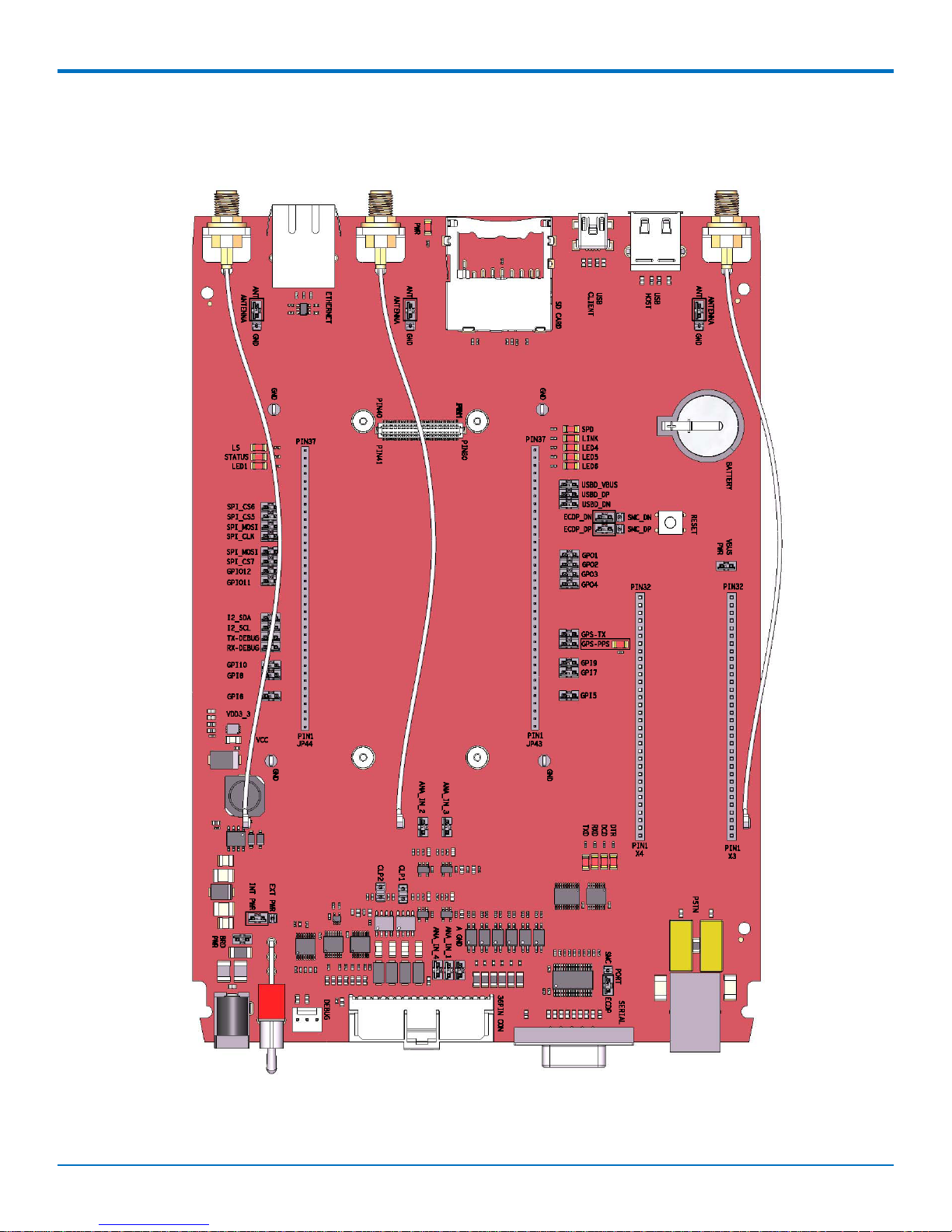
An illustration of the developer board follows.
MultiConnect® OCG-E MT100EOCG-EV3 Developer Guide 5
Page 6
DEVELOPER’S KIT AND DEVELOPER’S BOARD OVERVIEW
6 MultiConnect® OCG-E MT100EOCG-EV3 Developer Guide
Page 7
DEVELOPER’S KIT AND DEVELOPER’S BOARD OVERVIEW
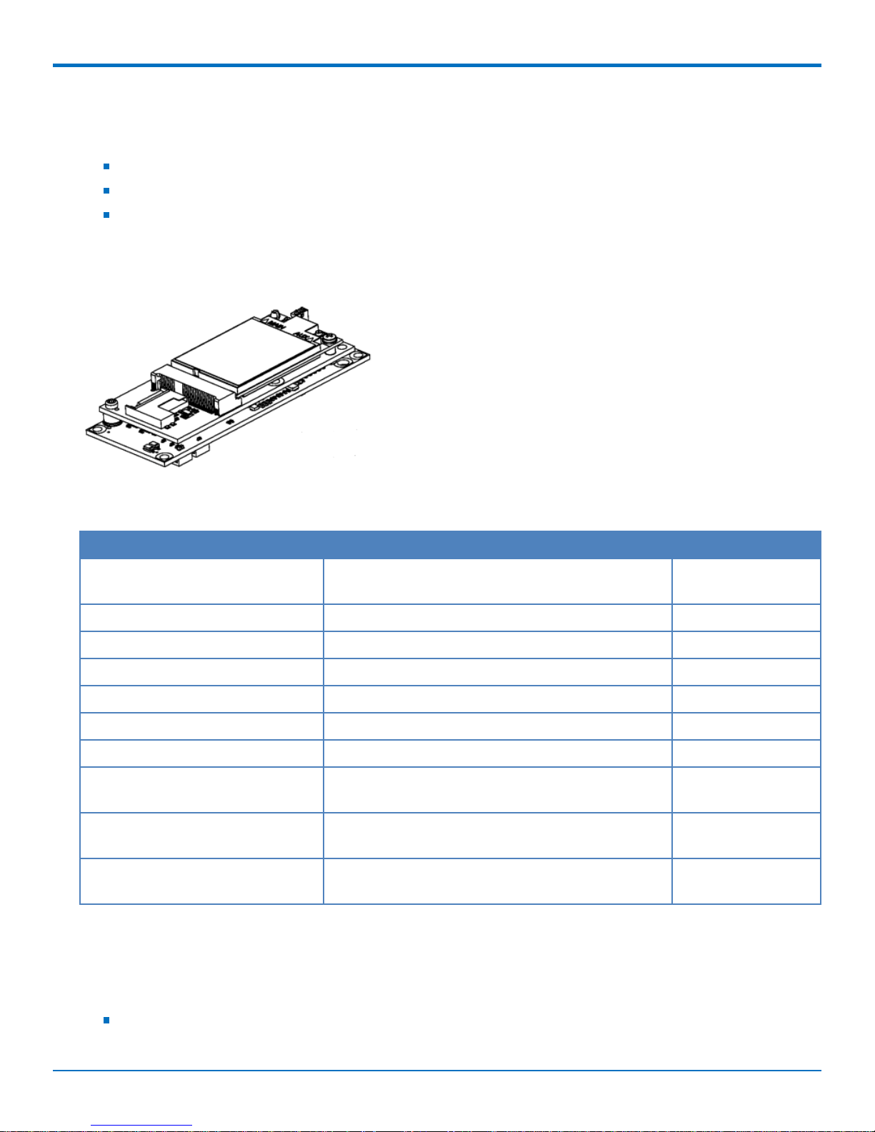
The developer’s board is available without a cellular modem. You can also develop your solution by choosing an
MT100EOCG model that uses the standard you desire:
GPRS, by selecting the MT100EOCG-G2 model
HSPA or HSDPA, by selecting the MT100EOCG-H5 model
EV-DO Rev A, by selecting the MT100EOCG-EV3 model
For complete ordering details, see the section “Product Ordering Options” in this manual. An illustration of an
MT100EOCG gateway follows. Your gateway may look slightly different, depending on the type of model you select
(-G2, -H5, -EV3 or gateway without cellular modem).
Product Ordering Options
Product Description Region
MT100EOCG-G2 2G, GPRS Embedded Open Communications
Gateway (OCG)
MT100EOCG-G2-GP 2G, GPRS Embedded OCG with GPS Global
MT100EOCG-H5 3G, HSPA Embedded OCG Global
MT100EOCG-H5-GP 3G, HSPA Embedded OCG with GPS Global
MT100EOCG-EV3-N3 3G, EV-DO Embedded OCG with GPS, Verizon US
MT100EOCG-EV3-N16 3G, EV-DO Embedded OCG, Aeris US
MT100EOCG-EV3-GP N16 3G, EV-DO Embedded OCG with GPS, Aeris US
MT100EOCG Open Communications Gateway without cellular
modem
MT100EOCG-GP Open Communications Gateway without cellular
modem, with GPS
MT100EOCG-DK Embedded OCG Developer Kit – Includes all cables
and Core CDP DVD
Global
Global
Global
Global
Developer’s Kit Contents
Use the MultiConnect OCG-E Developer’s Kit MT100EOCG-DK and the models described in this guide to develop
and evaluate your products and applications. This kit contains:
One MT100EOCG-DK developer board
MultiConnect® OCG-E MT100EOCG-EV3 Developer Guide 7
Page 8

DEVELOPER’S KIT AND DEVELOPER’S BOARD OVERVIEW
Universal power supply:
100-240V 9V-1.7A changeable blade power supply
Three removable blades (US, EURO and UK)
Cables
One DB9 serial cable
One 3-pin serial cable (debug)
One USB host cable
One USB device cable
One 36-pin GPIO cable
One RJ-45 Ethernet cable
One RJ-11 phone cable
Antennas
Two hepta-band cellular antenns
One GPS antenna
One Wi-Fi/Bluetooth antenna
Antenna cables
Three SMA-to-UFL antenna cables
One RSMA-to-MMCX antenna cable
One 2GB SD memory card
One CoreCDP DVD
Four screws for mounting gateway to developer’s board
One Multi-Tech screwdriver
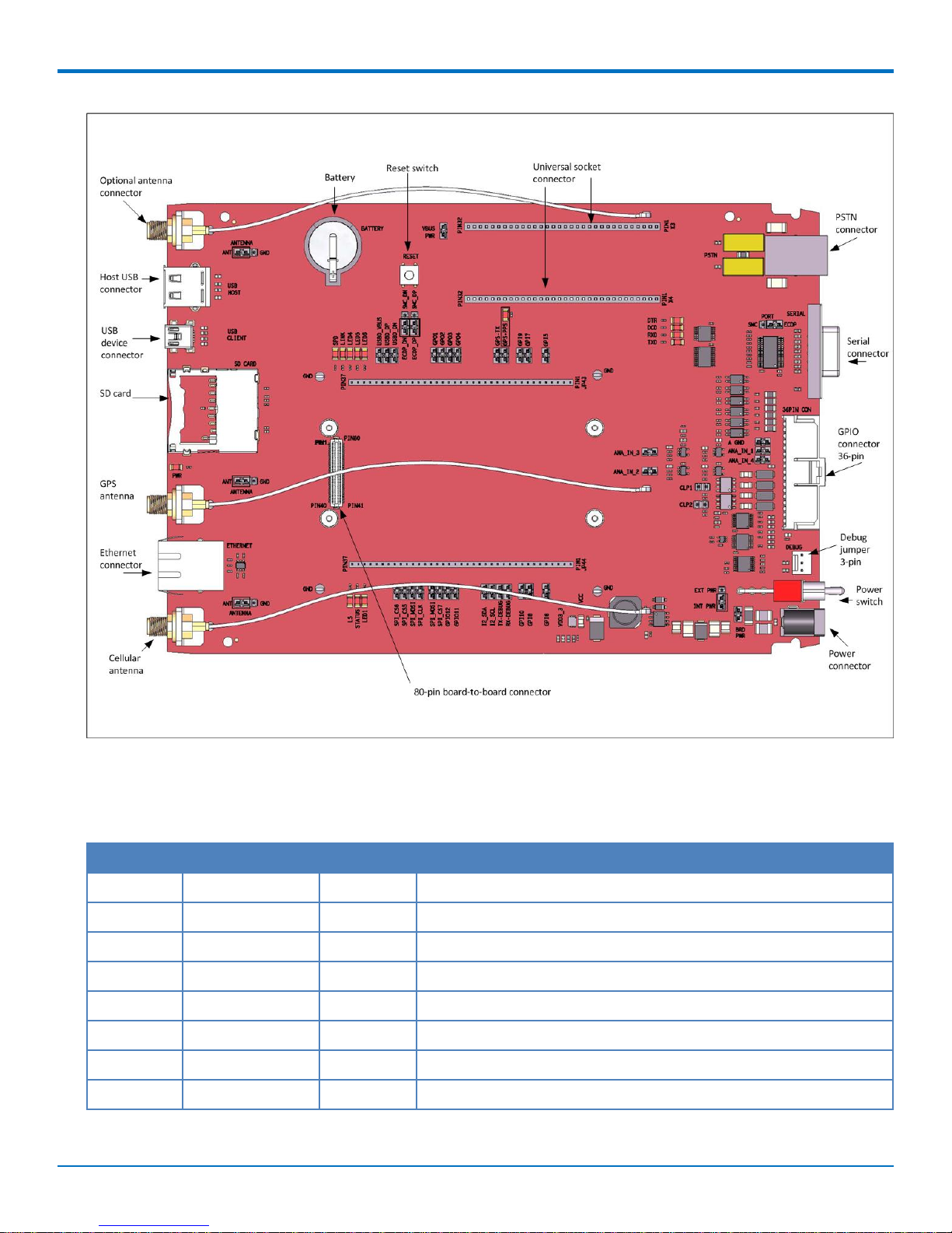
Developer’s Board Components
The developer board is an auxiliary board that helps you develop and debug products that use an embedded
MT100EOCG gateway. Using the developer board, you can connect the embedded MT100EOCG gateway to your
device.
The developer board provides multiple interfaces, such as USB, serial, Ethernet and SD card. The test points of key
signals are led out on the developer board. In addition, the board is designed with switches or pins of commonly
used signals such as the reset signal and the enable signal for converting the working state of the gateway. You can
use the board to test the performance of the gateway.
You can implement both the wired connection test and the wireless connection test (connect the gateway model
to the antennas). You can also test the signal points when you maintain and repair the gateway.
The board provides two, universal socket connectors that give you the option to develop and test your solutions
that might include Wi-Fi or other types of technologies.
8 MultiConnect® OCG-E MT100EOCG-EV3 Developer Guide
Page 9
DEVELOPER’S KIT AND DEVELOPER’S BOARD OVERVIEW
Pin Descriptions of Board to Board Connector
The MultiConnect OCG-E gateway connects to the developer board using an 80-pin board to board connector. This
section describes the connector’s pins.
Pin Signal Name In/Out Description
1 VCC I DC Input Power. 5V DC power.
2 VCC I DC Input Power. 5V DC power.
3 VCC I DC Input Power. 5V DC power.
4 GND Logic Ground.
5 SD_CLK O SDIO Clock.
6 SD_CMD O SDIO command.
7 SD_DAT0 I/O SDIO Data0.
8 GPI5 I General-Purpose Input.
MultiConnect® OCG-E MT100EOCG-EV3 Developer Guide 9
Page 10

DEVELOPER’S KIT AND DEVELOPER’S BOARD OVERVIEW
Pin Signal Name In/Out Description
9 ADC0 I Analog-to-Digital converter Input. (0 to 3v).
10 ADC2 I Analog-to-Digital converter Input. (0 to 3v).
11 GPI7 I General-Purpose Input.
12 GPI9 I General-Purpose Input.
13 TDO O JTAG Data Output.
14 NTRST I/O JTAG Reset (Active Low).
15 GPS-PPS O GPS PPS - Pulse Per Second.
16 GPS-TX O GPS - Transmit Data.
17 -DTR_1 I Data Terminal ready. The DTE uses the -DTR_1 line to signal to the
module that it is ready to accept communication. The signal is also
used to signal to the module to terminate communication (hangup).
18 -RXD_1 O Received Data. The gateway uses the RXD1 line to send data to
the DTE and to send gateway responses to the DTE. In command
mode, -RXD1 data presents the gateway responses to the DTE.
19 -TXD_1 I Transmitted Data. The DTE uses the -TXD1 line to send data to the
gateway for transmission or to transmit commands to the
gateway. The DTE holds this circuit in mark state when no data is
being transmitted or during intervals between characters.
20 -RTS_1 I "Request to Sent (Active Low). -RTS1 signal is used for hardware
flow control. -RTS1 input ON (low) indicates that the DTE is ready
to send data to the device. In the command state, the device
ignores -RTS1.
21 -DCD_1 O Data Carrier Detect (Active Low). DCD is controlled by processor.
You can program how DCD is set.
22 -CTS_1 O Clear to Send (Active Low). -CTS_1 is controlled by the gateway to
indicate whether or not the gateway is ready to receive data from
the DTE on the -TXD_1 input signal.
23 GPO4 O General-Purpose Output.
24 GPO3 O General-Purpose Output.
25 GPO2 O General-Purpose Output.
26 GPO1 O General-Purpose Output.
27 27 GND Logic Ground.
28 -RESET I Device Reset (with pull-up). The active low -RESET input resets the
device logic. -RESET is tied to VCC through a time-constant circuit
for proper reset of the device if -RESET is not being externally
driven.
29 BATT-IN I Battery Backup Input 3V.
30 USBH_DP I/O USB Host Data Positive. Positive pin of USB data pair.
10 MultiConnect® OCG-E MT100EOCG-EV3 Developer Guide
Page 11

DEVELOPER’S KIT AND DEVELOPER’S BOARD OVERVIEW
Pin Signal Name In/Out Description
31 USBH_DN I/O USB Host Data Negative. Negative pin of USB data pair.
32 GND Logic Ground.
33 USBD_DN I/O USB Device Data Negative. Negative pin of USB data pair.
34 USBD_DP I/O USB Device Data Positive. Positive pin of USB data pair
35 USBD_VBUS I USB Device Voltage Sense. Senses the voltage level of the USB to
determine if the bus is available.
36 -LED_6 O General Purpose LED6 output (signal strength).
37 -LED_5 O General Purpose LED5 output (signal strength).
38 -LED_4 O General Purpose LED4 output (signal strength).
39 -LED_7 O Ethernet link.
40 -LED_8 O Ethernet speed.
41 EVDDA O 3.3V analog supply for Ethernet transformer.
42 ERX- I Receive Input Negative. Differential receive input pin for Ethernet.
43 ERX+ I Receive Input Positive. Differential receive input pin for Ethernet.
44 ETX- O Transmit Output (negative). Differential transmit output for
Ethernet.
45 ETX+ O Transmit Output (positive). Differential transmit output for
Ethernet.
46 GND Logic Ground.
47 N_SD_PROTECT I SD Card Detection input.
48 TMS I JTAG Test Mode Select.
49 SPI_CS6 O SPI Chip Select 6.
50 SPI_CS5 O SPI Chip Select 5.
51 SPI_MOSI O SPI Master-Out.
52 SPI_CLK O SPI Clock.
53 GND Logic Ground.
54 SPI_MISO I SPI Master-In.
55 SPI_CS7 O SPI Chip Select 7.
56 N_SD_DETECT I SD Card Detection input.
57 GPIO12 I/O General-Purpose Input/Output. User-configurable input or output
58 GPIO11 I/O General-Purpose Input/Output. User-configurable input or output
59 RTCK O JTAG Returned JTAG Clock.
60 -LED_3 O General Purpose LED3 output (Link staus output).
MultiConnect® OCG-E MT100EOCG-EV3 Developer Guide 11
pin.
pin.
Page 12

DEVELOPER’S KIT AND DEVELOPER’S BOARD OVERVIEW
Pin Signal Name In/Out Description
61 -LED_2 O General Purpose LED2 output. (status).
62 -LED_1 O General Purpose LED1 output.
63 SDA I/O I2C Data.
64 SCL O I2C Clock.
65 -TXD-Debug I Transmitted Data. The DTE uses the -TXD3 line to send data to the
gateway for transmission of Debug information.
66 -RXD-Debug O Received Data. The gateway uses the RXD-debug line to send data
to a DTE for debug purposes.
67 TCK I I JTAG Clock.
68 TDI I JTAG Data Input.
69 GPI10 I General-Purpose Input.
70 GPI8 I General-Purpose Input.
71 ADC3 I Analog-to-Digital converter Input (0 to 3v).
72 ADC1 I Analog-to-Digital converter Input (0 to 3v).
73 GPI6 I General-Purpose Input.
74 SD_DAT3 I/O SDIO Data3.
75 SD_DAT2 I/O SDIO Data2.
76 I/O SDIO Data1.
77 SD_DAT1 I/O GND Logic Ground.
78 VCC I DC Input Power. 5V DC power.
79 VCC I DC Input Power. 5V DC power.
80 VCC I DC Input Power. 5V DC power.
12 MultiConnect® OCG-E MT100EOCG-EV3 Developer Guide
Page 13

Block Diagram
DEVELOPER’S KIT AND DEVELOPER’S BOARD OVERVIEW
MultiConnect® OCG-E MT100EOCG-EV3 Developer Guide 13
Page 14
DEVELOPER’S KIT AND DEVELOPER’S BOARD OVERVIEW
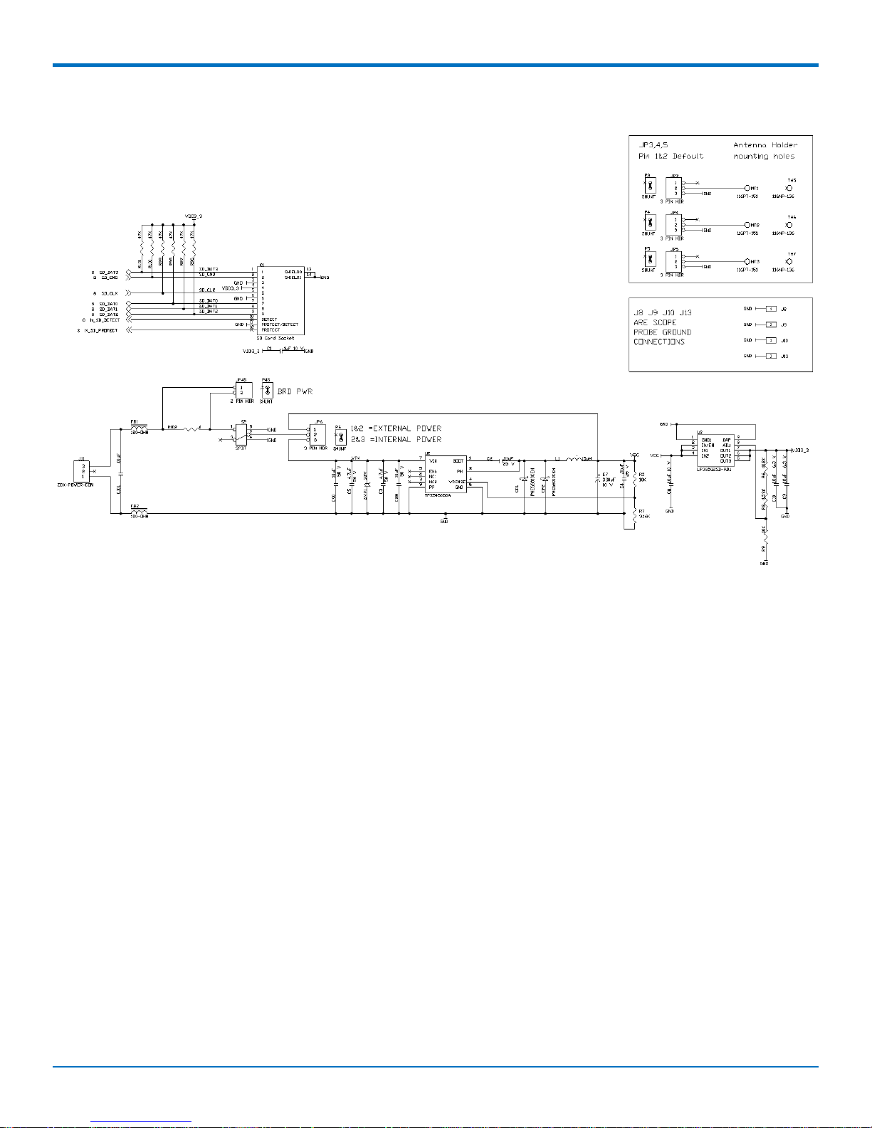
Schematic 1
14 MultiConnect® OCG-E MT100EOCG-EV3 Developer Guide
Page 15
Schematic 2
DEVELOPER’S KIT AND DEVELOPER’S BOARD OVERVIEW
MultiConnect® OCG-E MT100EOCG-EV3 Developer Guide 15
Page 16

DEVELOPER’S KIT AND DEVELOPER’S BOARD OVERVIEW
Schematic 3
16 MultiConnect® OCG-E MT100EOCG-EV3 Developer Guide
Page 17

Schematic 4
DEVELOPER’S KIT AND DEVELOPER’S BOARD OVERVIEW
MultiConnect® OCG-E MT100EOCG-EV3 Developer Guide 17
Page 18

DEVELOPER’S KIT AND DEVELOPER’S BOARD OVERVIEW
Schematic 5
18 MultiConnect® OCG-E MT100EOCG-EV3 Developer Guide
Page 19

Schematic 6
DEVELOPER’S KIT AND DEVELOPER’S BOARD OVERVIEW
MultiConnect® OCG-E MT100EOCG-EV3 Developer Guide 19
Page 20

DEVELOPER’S KIT AND DEVELOPER’S BOARD OVERVIEW
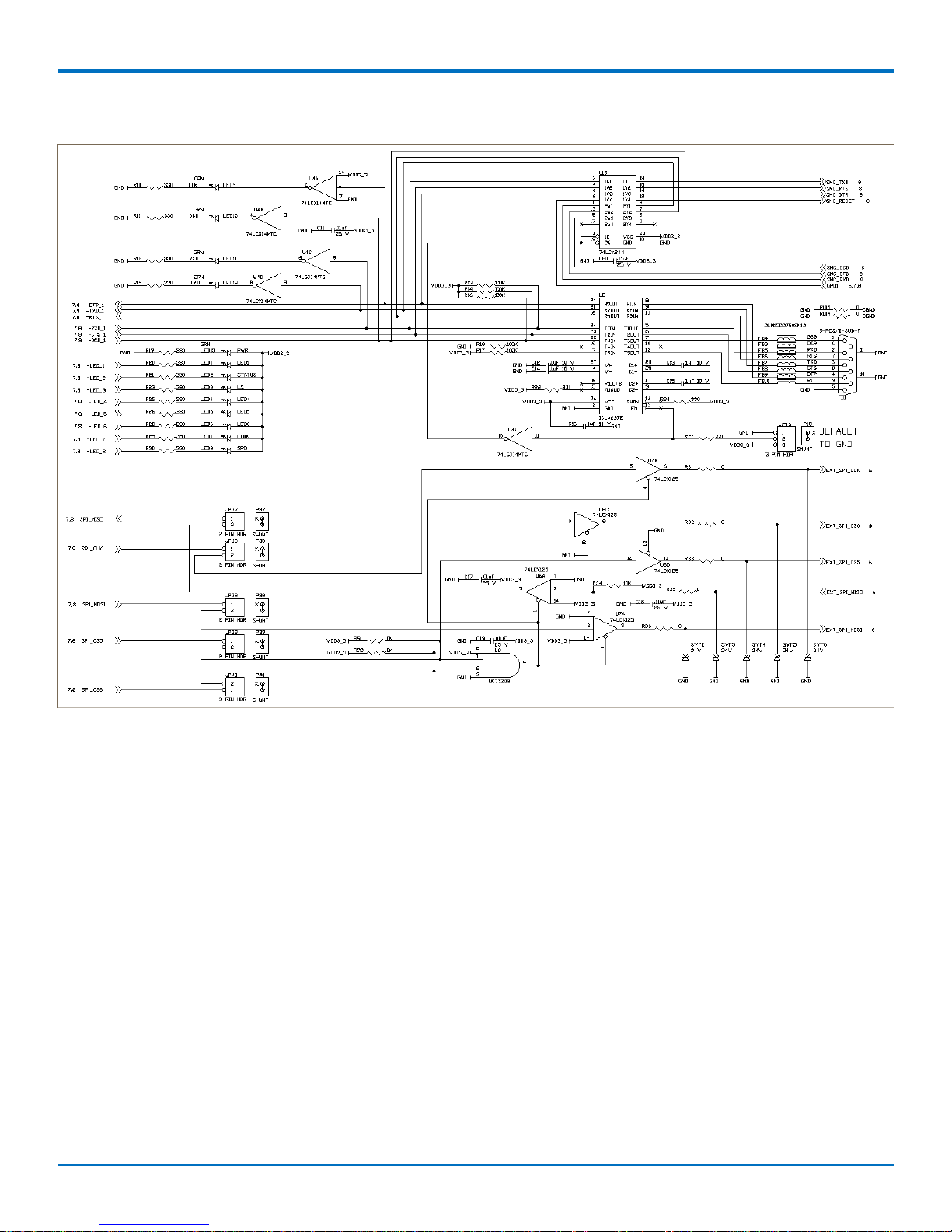
Schematic 7
Technical Specifications
All models of the MultiConnect OCG-E gateway share the following specifications. Specifications that are unique to
a particular model are documented in the chapter dedicated to the model.
Category Description
Operating Voltage 5VDC +/- 10%
Dimensions 3.650" x 1.375" (92 mm x 34.925 mm)
Storage Environment -40° to +85° C
Humidity 20% to 90% non-condensing
Warranty 2 years
20 MultiConnect® OCG-E MT100EOCG-EV3 Developer Guide
Page 21

DEVELOPER’S KIT AND DEVELOPER’S BOARD OVERVIEW
MT100EOCG-DK LEDs Description
LED 1 General Purpose LED1 output.
LED 2 General Purpose LED2 output (status).
LED 3 General Purpose LED3 output (link status).
LED 4 General Purpose LED4 output.
LED 5 General Purpose LED5 output.
LED 6 General Purpose LED6 output.
LED 7 Ethernet link.
LED 8 Ethernet speed.
LED 9 DTR.
LED 10 DCD.
LED 11 RXD.
LED 12 TXD.
LED 13 POWER.
Logging into the MultiConnect OCG-E Gateway
To log into the MultiConnect OCG-E gateway and open the modem port, use SSH or the debug serial port.
1. To use SSH to log into the gateway:
The default IP address is 192.168.2.1.
The default username and password are: root and root.
2. To use the debug serial port:
The debug port serial settings are 115200 baud, 8N1, with no flow control.
The default username and password are: root and root.
Safety Notices and Warnings
This section describes safety statements that OEMs can use in their product documentation.
Radio Frequency (RF) Safety
Due to the possibility of radio frequency (RF) interference, it is important that you follow any special regulations
regarding the use of radio equipment. Follow the safety advice given below.
Operating your device close to other electronic equipment may cause interference if the equipment is
inadequately protected. Observe any warning signs and manufacturers’ recommendations.
Different industries and businesses restrict the use of cellular devices. Respect restrictions on the use of
radio equipment in fuel depots, chemical plants, or where blasting operations are in process. Follow
restrictions for any environment where you operate the device.
Do not place the antenna outdoors.
MultiConnect® OCG-E MT100EOCG-EV3 Developer Guide 21
Page 22

DEVELOPER’S KIT AND DEVELOPER’S BOARD OVERVIEW
Switch OFF your wireless device when in an aircraft. Using portable electronic devices in an aircraft may
endanger aircraft operation, disrupt the cellular network, and is illegal. Failing to observe this restriction
may lead to suspension or denial of cellular services to the offender, legal action, or both.
Switch OFF your wireless device when around gasoline or diesel-fuel pumps and before filling your vehicle
with fuel.
Switch OFF your wireless device in hospitals and any other place where medical equipment may be in use.
Vehicle Safety
When using your device in a vehicle:
Do not use this device while driving.
Respect national regulations on the use of cellular devices in vehicles.
If incorrectly installed in a vehicle, operating the wireless device could interfere with the vehicle’ s
electronics. To avoid such problems, use qualified personnel to install the device. The installer should verify
the vehicle electronics are protected from interference.
Using an alert device to operate a vehicle’s lights or horn is not permitted on public roads.
UL evaluated this device for use in ordinary locations only. UL did NOT evaluate this device for installation in
a vehicle or other outdoor locations. UL Certification does not apply or extend to use in vehicles or outdoor
applications.
Device Maintenance
When maintaining your device:
Do not attempt to disassemble the device. There are no user serviceable parts inside.
Do not misuse the device. Follow instructions on proper operation and only use as intended. Misuse could
make the device inoperable, damage the device and/or other equipment, or harm users.
Do not apply excessive pressure or place unnecessary weight on the device. This could result in damage to
the device or harm to users .
Do not use this device in explosive or hazardous environments unless the model is specifically approved for
such use. The device may cause sparks. Sparks in explosive areas could cause explosion or fire and may
result in property damage, severe injury, and/or death.
Do not expose your device to any extreme environment where the temperature or humidity is high. Such
exposure could result in damage to the device or fire.
Do not expose the device to water, rain, or spilled beverages. It is not waterproof. Exposure to liquids could
result in damage to the device.
Do not place the device alongside computer discs, credit or travel cards, or other magnetic media. The
information contained on discs or cards may be affected by the device.
Using accessories, such as antennas, that MultiTech has not authorized or that are not compliant with
MultiTech's accessory specifications may invalidate the warranty.
If the device is not working properly, contact MultiTech Technical Support.
Handling Precautions
To avoid damage due to the accumulation of static charge, use proper precautions when handling any cellular
device. Although input protection circuitry has been incorporated into the devices to minimize the effect of static
22 MultiConnect® OCG-E MT100EOCG-EV3 Developer Guide
Page 23

DEVELOPER’S KIT AND DEVELOPER’S BOARD OVERVIEW
build-up, use proper precautions to avoid exposure to electronic discharge during handling and mounting the
device.
Securing Your Device
Respect all local regulations. Become familiar with and use the security features to block unauthorized use and
theft.
MultiConnect® OCG-E MT100EOCG-EV3 Developer Guide 23
Page 24

INSTALLING GATEWAYS ON THE DEVELOPER BOARD
Chapter 2 – Installing Gateways on the Developer
Board
Installing Gateways on the Developer Board
These topics describe how to install gateways on the developer board. You can install a Multi-Connect OCG-E
gateway or, optionally, a universal socket communications device.
Installing a MultiConnect OCG-E Gateway onto the Board
To install a MultiConnect OCG-E gateway:
1. Align the 80-pin connector on the bottom of the gateway with the 80-pin connector on the developer
board.
2. Press the 80-pin connector of the gateway firmly into the 80-pin connector on the developer board.
Ensure that the mounting holes on the ends of the gateway align with the four standoffs on the
developer board.
24 MultiConnect® OCG-E MT100EOCG-EV3 Developer Guide
Page 25

INSTALLING GATEWAYS ON THE DEVELOPER BOARD
3. If you are installing a MultiConnect OCG-E gateway with a cellular wireless network, connect the cellular
antenna lead to the antenna connector on the MultiConnect OCG-E gateway.
4. If you are installing a MultiConnect OCG-E gateway with a GPS receiver, first connect the cellular antenna
lead to the cellular antenna connector on the gateway, then connect the GPS antenna lead to the GPS
antenna connector on the gateway.
Installing a Universal Socket Communications Device onto the Board
To install a SMI/SMC modem:
1. Align the pin of the universal socket communications device with pin 1 of the universal socket connector
on the board and press firmly. For details about the location of pin 1, see the illustration on page 20.
2. Use the optional antenna lead to connect to the antenna connector on the modem.
Installing a SIM Card onto the Board
To install a SIM card, if your model supports the use of a card:
1. Install the SIM card into the SIM card holder on the board.
Making Other Board Connections
1. If your application needs a power supply, connect the power supply lead to the power connector on the
developer board.
2. If you need to connect the debug cable for your application, connect the 3-pin connector of the debug
cable to the debug jumper next to the power switch.
3. If you need the GPIO cable in your application, connect the J1 connector on the GPIO cable to the 36-pin
connector on the developer board.
MultiConnect® OCG-E MT100EOCG-EV3 Developer Guide 25
Page 26

INSTALLING GATEWAYS ON THE DEVELOPER BOARD
General Purpose Input Output (GPIO) Cable
GPIO Connector Pin Out
Pin Number Name Input/Output Description
1 EXT_IN_0 I General-Purpose Input.
2 EXT_IN_1 I General-Purpose Input.
3 EXT_IN_2 I General-Purpose Input.
4 EXT_IN_3 I General-Purpose Input.
5 EXT_IN_4 I General-Purpose Input.
6 EXT_IN_5 I General-Purpose Input.
7 GPIO11 I/O General-Purpose Input/Output. User-configurable
8 GPIO12 I/O General-Purpose Input/Output. User-configurable
26 MultiConnect® OCG-E MT100EOCG-EV3 Developer Guide
input or output pin.
input or output pin.
Page 27

INSTALLING GATEWAYS ON THE DEVELOPER BOARD
Pin Number Name Input/Output Description
9 EXT_IN_GND GND Logic Ground from external.
10 A_GND_OUT GND Logic Ground from analog side of ADC.
11 ANA_IN_1 I Analog-to-Digital converter Input (0 to 3v).
12 ANA_IN_2 I Analog-to-Digital converter Input (0 to 3v).
13 ANA_IN_3 I Analog-to-Digital converter Input (0 to 3v).
14 ANA_IN_4 I Analog-to-Digital converter Input (0 to 3v).
15 EXT_OUT_GND GND Logic Ground to external.
16 EXT_OUT_GND GND Logic Ground to external.
17 EXT_OUT_0 O General-Purpose Output.
18 EXT_OUT_1 O General-Purpose Output.
19 EXT_OUT_2 O General-Purpose Output.
20 EXT_OUT_3 O General-Purpose Output.
21 NC No Connect.
22 NC No Connect.
23 NC No Connect.
24 SPI_CS7 O SPI Chip Select 7.
25 EXT_SPI_CLK O SPI Clock.
26 EXT_SPI_MISO I SPI Master-In.
27 EXT_SPI_MOSI O SPI Master-Out.
28 EXT_SPI_CS5 O SPI Chip Select 5.
29 EXT_SPI_CS6 O SPI Chip Select 6.
30 EXT_DB_RX O Received Data. The gateway uses the RXD=debug
line to send data to a DTE for debug purposes.
31 EXT_DB_TX I Transmitted Data. The DTE uses the -TXD3 line to
send data to the model for transmission of Debug
information.
32 GPS-PPS O GPS PPS - Pulse Per Second.
33 I2_SCL I/O I2C Clock.
34 I2_SDA I/O I2C Data.
35 GPS-TX O GPS PPS - Transmit Data.
36 GND GND Logic Ground.
Notes
The GPI and GPO pins use 74LV logic family for input and the 74LVC logic family for output.
GPI input range:
MultiConnect® OCG-E MT100EOCG-EV3 Developer Guide 27
Page 28

INSTALLING GATEWAYS ON THE DEVELOPER BOARD
> 2.3 V for a high
< 1V for a low
GPI pins are 5 V tolerant. GPI pins have a 10K pull-downs to ground. This increases the input current to 330 uA
from the standard 1uA.
GPO pins output range:
> 2.58 V@4ma is a high
<= .36 V @4ma is a low
Maximum current on a GPO pin is +25 mA not to exceed 70ma total for all 4 GPO.
GPIO11 / GPIO 12 and SPI/I2C pins:
These are directly connected to the processor.
If the pin is programmed as an output, the high is 2.9V minimum and low is 0.4V maximum with a maximum
current draw of 8 mA. If the pin is programmed as an input, a high must be greater than 2.3V and a low
must be less than 1V.
These pins also have an optional pull-up resistor with a range of 40k ohm to 190k ohm, with a typical value
of 75k ohm.
Otherwise the input leakage is 1 uA.
Additional hardware is needed to drive the I2E and SPI signals if any additional wire is added to the signals.
For the I2C there are bus repeaters available that would be suitable, for example, Texas Instruments
LEVEL-TRANSLATING I2C BUS REPEATER PCA9517.
For the SPI signal, any logic level buffer that works at 3.3V would work.
LED Signals
GPO1-GPO4,LED1, and LED4-LED6 are sourced from the same IC.
Each pin can source 25 mA, but all pins, 4 GPO and 4 LED, can only source 70 mA total. This means the
cumulative output current of those pins is limited by the maximum output current rating of the IC.
GPO1-4 each can drive +25 mA, but total for all four is 70 mA (25 mA * 4 = 100 mA, but it cannot drive
that much all at the same time). It also means that if the IC dies, then all of those outputs die.
LED2 is directly connected to the processor GPIO pin PA30 and has the same characteristics as GPIO11
and GPIO12. The default operation of LED2 in CoreCDP is as a Linux Status indicator.
LED3 is sourced by a LVC open drain buffer and has a max current draw of 32 mA. LED3 is directly
connected to the Link Status pin of the device and is therefore dedicated.
LED7 and LED8 are driven directly by the Ethernet PHY chip and can drive about 4 mA. They are usually
used for Ethernet speed, link, and activity indicators.
28 MultiConnect® OCG-E MT100EOCG-EV3 Developer Guide
Page 29

INSTALLING GATEWAYS ON THE DEVELOPER BOARD
Debug Cable
MT100EOCG Electrical Characteristics
Operating Conditions Units Volts
Parameter Minimum Maximum
Supply Range - Vcc 4.5 5.5
Absolute Maximum Rating Units Volts
Parameter Minimum Maximum
Voltage at any signal pin -0.3 3.6
Reset -0.3 5.5
SPI -0.3 3.6
ADC Operating Range Units Volts
ADC input operating range 0 3
DC Electrical Characteristics GPIO1-4/GP15-10/LED1,4,5,6 Units - Volts
Parameter Minimum Maximum
Digital signal output low level 0.36
Digital signal output high level 2.58
Digital signal input low level 0.8
Digital signal input high level 2.3
DC Electrical Characteristics SPI/SD Flash Card Interface/JTAG/GPS-TX/Serial Ports/I2C/-LED2/GPIO11,12 SD
Flash Card Status - Units - Volts
Parameter Minimum Maximum
Digital signal output low level 0.4
Digital signal output high level 2.9
Digital signal input low level 0.8
Digital signal input high level 2.3
DC Electrical Characteristics GPS-PPS/-LED7,8 Unit - Volts
MultiConnect® OCG-E MT100EOCG-EV3 Developer Guide 29
Page 30

INSTALLING GATEWAYS ON THE DEVELOPER BOARD
Parameter Minimum Maximum
Digital signal output low level 0.4
Digital signal output high level 2.4
DC Electrical Characteristics-LED3 Unit - Volts
Output is open drain with 10k pullup
DC Electrical Characteristics Reset Unit - Volts
Parameter Minimum Maximum
Reset (low active) input low 0.8
Reset (low active) input high 2.3
DC Electrical Characteristics USB Device Port
Standard USB 2.0 Full Speed Device Port
Pin 35 USBD VBUS 5V input for detection of USB bus availability
DC Electrical Characteristics USB Host Port
Standard USB 2.0 Full Speed Host Port
Digital Input Capacitance
30 MultiConnect® OCG-E MT100EOCG-EV3 Developer Guide
Page 31

TROUBLESHOOTING
Chapter 3 – Troubleshooting
Restoring the U-Boot Memory or the Bootstrap Memory
If the U-boot memory or the bootstrap memory becomes corrupted, you can restore either of them.
Before You Begin
You need to short out a resistor to run internal boot code instead of code in bootstrap or u-boot memory. To do
this, find some tweezers that fit around the resistor. You also need to download a utility to help you restore
memory. To do so:
1. Download Atmel SAM-BA utility from the following location: http://www.atmel.com/tools/ATMELSAM-
BAIN-SYSTEMPROGRAMMER.aspx
2. Unzip the utility package onto your Linux development system.
Restoring Memory Overview
1. Power down.
2. Short out the R108 resistor by squeezing it with tweezers.
3. Restore power.
4. Remove tweezers from the resistor.
5. Restore the bootstrap memory or the u-boot memory. The following sections describe these steps in
greater detail.
Shorting the R108 Resistor
To access the internal boot code directly, first short the R108 resistor so the boot code and u-memory code do not
run.
1. Power off the device.
2. Locate the R108 resistor on the board. The following figure shows the location of the resistor.
3. Place tweezers around the R108 resistor and squeeze the resistor, to short it out.
4. Power on the device.
5. Remove tweezers.
MultiConnect® OCG-E MT100EOCG-EV3 Developer Guide 31
Page 32

TROUBLESHOOTING
Installing Atmel SAM-BA Utility
This topic describes how to restore memory by using the Atmel SAM-BA utility, connecting with the hardware,
mounting the serial driver and restoring the bootstrap memory or u-boot memory.
1. If you have not already done so, download the Atmel SAM-BA utility and unzip the utility package onto
your Linux development system: http://www.atmel.com/tools/ATMELSAM-BAINSYSTEMPROGRAMMER.aspx
2. Connect the USB cable between Linux system and the MTEOCG hardware.
3. Mount the USB CDC serial driver as described in the topic for the Ubuntu operating system you are using.
Mounting USB CDC serial driver for Ubuntu version 9.10 and older
1. Log in with administrator rights.
2. If the usbserial and cdc_acm module is already running, unload it by using the following command:
# rmmod cdc_acm
# rmmod usbserial
3. To load the usbserial kernel module, type:
1 #modprobe usbserial vendor=0x03eb product=0x6124
4. To verify that the USB connection is established, type:
#lsusb -d 03eb:6124
5. To determine which USB connection is established, type:
#dmesg
...
kernel: usb 4-2: new full speed USB device using uhci_hcd and address 5
kernel: usb 42: configuration #1 chosen from 1 choice kernel: usbserial_generic 42:1.0: generic converter detected
kernel: usbserial_generic: probe of 4-2:1.0 failed with error -5
kernel: usbserial_generic 4-2:1.1: generic converter detected
kernel: usb 4-2: generic converter now attached to ttyUSBx
6. To connect to your board, use /dev/ttyUSBx .
Mounting USB CDC serial driver for Ubuntu 10.04 and newer with updated kernel
1. If you are using a 64-bit system, type the following to ensure 32-bit libraries are installed:
sudo apt-get install ia32-libs
2. To ensure that the abstract control model (ACM) device was detected and to check the port name:
#dmesg
...
kernel: usb 41: new full speed USB device using ohci_hcd and address 2
kernel: usb 4-1: configuration #1 chosen from 1 choice
kernel: cdc_acm 41:1.0: This device cannot do calls on its own. It is not a modem.
kernel: cdc_acm 4-1:1.0: ttyACM0: USB ACM device
kernel: usbcore: registered new interface driver cdc_acm
32 MultiConnect® OCG-E MT100EOCG-EV3 Developer Guide
Page 33

TROUBLESHOOTING
kernel: cdc_acm: v0.26:USB Abstract Control Model driver for USB modems
and ISDN adapters
3. To connect to your board, use /dev/ttyACMX.
Using the Atmel SAM-BA utility to restore memory
1. To run the utility, type: # ./sam-ba
2. Select your board at91sam9g20-ek and click Connect.
3. Select NandFlash.
4. Select the Enable NandFlash script and execute it.
5. Make sure the script executed successfully, otherwise the steps that follow do not work.
Restoring U-Boot Memory
To restore the u-boot memory:
1. Set the address to 0×20000.
2. Open and select Send File Name. Open the uboot bin file.
3. Click Send File.
4. Make sure the uboot bin file is programmed successfully. To check, click Compare Sent File with Memory
and ensure the file and memory match.
Restoring Bootstrap Memory
To restore the bootstrap memory:
1. Select the Send Boot File script and execute.
2. Select the bootstrap file to program.
3. Make sure bootstrap is programmed successfully.
MultiConnect® OCG-E MT100EOCG-EV3 Developer Guide 33
Page 34

DESIGN CONSIDERATIONS
Chapter 4 – Design Considerations
Noise Suppression Design
Adhere to engineering noise-suppression practices when designing a printed circuit board (PCB). Noise suppression
is essential to the proper operation and performance of the modem and surrounding equipment.
Any OEM board design must consider both on-board and off-board generated noise that can affect digital signal
processing. Both on-board and off-board generated noise that is coupled on-board can affect interface signal levels
and quality. Noise in frequency ranges that affect modem performance is of particular concern.
On-board generated electromagnetic interference (EMI) noise that can be radiated or conducted off-board is
equally important. This type of noise can affect the operation of surrounding equipment. Most local government
agencies have certification requirements that must be met for use in specific environments.
Proper PC board layout (component placement, signal routing, trace thickness and geometry, and so on)
component selection (composition, value, and tolerance), interface connections, and shielding are required for the
board design to achieve desired modem performance and to attain EMI certification.
Other aspects of proper noise-suppression engineering practices are beyond the scope of this guide. Consult noise
suppression techniques described in technical publications and journals, electronics and electrical engineering text
books, and component supplier application notes.
PC Board Layout Guideline
In a 4-layer design, provide adequate ground plane covering the entire board. In 4-layer designs, power and ground
are typically on the inner layers. Ensure that all power and ground traces are 0.05 inches wide.
The recommended hole size for the device pins is 0.036 in. +/-0.003 in. in diameter. Use spacers to hold the device
vertically in place during the wave solder process.
All creepages and clearances for the device meet requirements of safety standards listed in the technical
specifications. The requirements are based on a working voltage of 125V or 250V. When implementing the
recommended DAA* circuit interface in a third party design, strictly follow all creepage and clearance
requirements to meet safety standards. The third party safety design must be evaluated by the appropriate
national agency according to the required specification.
User Accessible Areas
Based on where the third party design is marketed, sold, or used, it may be necessary to provide an insulating
cover over all TNV exposed areas. Consult with the recognized safety agency to determine the requirements.
Note: Even if the recommended design considerations are followed, there are no guarantees that a particular
system complies with all the necessary regulatory requirements. Make sure a qualified and recognized agency
evaluates specific designs. .
*DAA stands for Data Access Arrangement. DAA is the device's telephone line interface.
Mounting Hardware
When mounting modems to the board, use #4 or M2/M3 hardware.
34 MultiConnect® OCG-E MT100EOCG-EV3 Developer Guide
Page 35

DESIGN CONSIDERATIONS
Electromagnetic Interference
The following guidelines are offered specifically to help minimize EMI generation. Some of these guidelines are the
same as, or similar to, the general guidelines. To minimize the contribution of device-based design to EMI, you
must understand the major sources of EMI and how to reduce them to acceptable levels.
Keep traces carrying high frequency signals as short as possible.
Provide a good ground plane or grid. In some cases, a multilayer board may be required with full layers for
ground and power distribution.
Decouple power from ground with decoupling capacitors as close to the device's power pins as possible.
Eliminate ground loops, which are unexpected current return paths to the power source and ground.
Decouple the telephone line cables at the telephone line jacks. Typically, use a combination of series
inductors, common mode chokes, and shunt capacitors. Methods to decouple telephone lines are similar to
decoupling power lines; however, telephone line decoupling may be more difficult and deserves additional
attention. A commonly used design aid is to place footprints for these components and populate as
necessary during performance/EMI testing and certification.
Decouple the power cord at the power cord interface with decoupling capacitors. Methods to decouple
power lines are similar to decoupling telephone lines.
Locate high frequency circuits in a separate area to minimize capacitive coupling to other circuits.
Locate cables and connectors to avoid coupling from high frequency circuits.
Lay out the highest frequency signal traces next to the ground grid.
If using a multilayer board design, make no cuts in the ground or power planes and be sure the ground
plane covers all traces.
Minimize the number of through-hole connections on traces carrying high frequency signals.
Avoid right angle turns on high frequency traces. Forty-five degree corners are good; however, radius turns
are better.
On 2-layer boards with no ground grid, provide a shadow ground trace on the opposite side of the board to
traces carrying high frequency signals. This will be effective as a high frequency ground return if it is three
times the width of the signal traces.
Distribute high frequency signals continuously on a single trace rather than several traces radiating from
one point.
Electrostatic Discharge Control
Handle all electronic devices with precautions to avoid damage due to the static charge accumulation.
See the ANSI/ESD Association Standard (ANSI/ESD S20.20-1999) – a document “for the Development of an
Electrostatic Discharge Control for Protection of Electrical and Electronic Parts, Assemblies and Equipment.” This
document covers ESD Control Program Administrative Requirements, ESD Training, ESD Control Program Plan
Technical Requirements (grounding/bonding systems, personnel grooming, protected areas, packaging, marking,
equipment, and handling), and Sensitivity Testing.
MultiTech strives to follow these recommendations. Input protection circuitry is incorporated in MultiTech devices
to minimize the effect of static buildup. Take precautions to avoid exposure to electrostatic discharge during
handling.
MultiConnect® OCG-E MT100EOCG-EV3 Developer Guide 35
Page 36

DESIGN CONSIDERATIONS
MultiTech uses and recommends that others use anti-static boxes that create a faraday cage (packaging designed
to exclude electromagnetic fields). MultiTech recommends that you use our packaging when returning a product
and when you ship your products to your customers.
36 MultiConnect® OCG-E MT100EOCG-EV3 Developer Guide
Page 37

OEM INTEGRATION
Chapter 5 – OEM Integration
FCC Grant Notes
The OEM should follow all the grant notes listed below. Otherwise, further testing and device approvals may be
necessary.
The antenna gain, including cable loss, for the radio you are incorporating into your product design must not
exceed the requirements at 850 MHz and 1900 MHz as specified by the FCC grant for mobile operations and fixed
mounted operations as defined in 2.1091 and 1.1307 of the FCC rules for satisfying RF exposure compliance. Power
output listed is conducted.
This device is a mobile device with respect to RF exposure compliance. The antenna(s) used for this transmitter
must be installed to provide a separation distance of at least 20 cm from all persons, and must not be collocated or
operate in conjunction with any other antenna or transmitter except in accordance with FCC multi-transmitter
product guidelines. Installers and end-users must be provided with specific information required to satisfy RF
exposure compliance for installations and final host devices. (See note under Grant Limitations.) Compliance of this
device in all final host configurations is the responsibility of the Grantee.
Grant Limitations
This device has been granted modular approval for mobile applications. Portable applications may require further
RF exposure (SAR) evaluations. Examples of mobile devices include wireless routers, desktop computers, utility
meters, etc. Examples of portable applications include devices such as a laptop, USB dongle, mobile phone, tablet
PC, and any device that can be worn on the body during use.
Your final product with this embedded device may need to pass FCC Part 15B.
This device has not been evaluated or approved for simultaneous transmission. Any simultaneous transmission
conditions should be evaluated per the current FCC KDB 447498 requirements. Simultaneous transmission
requirements for mobile devices are contained in Section 8.
KDB 447498 Section 8
Transmitters and modules certified for mobile or portable exposure conditions and categorically excluded by §
2.1091(c) can be incorporated in mobile host devices without further testing or certification when:
The closest separation among all simultaneous transmitting antennas is ≥ 20 cm;
or
The antenna separation distance and MPE compliance boundary requirements that enable all simultaneous
transmitting antennas incorporated within the host to comply with MPE limits are specified in the application
filing of at least one of the certified transmitters incorporated in the host device. In addition, when
transmitters certified for portable use are incorporated in a mobile host device the antenna(s) must be ≥ 5 cm
from all other simultaneous transmitting antennas. All antennas in the final product must be at least 20 cm
from users and nearby persons.
If the host device requires further authorization, consult an accredited FCC laboratory for guidance.
FCC Definitions
Portable: (§2.1093) — A portable device is defined as a transmitting device designed to be used so that the
radiating structure(s) of the device is/are within 20 centimeters of the body of the user.
MultiConnect® OCG-E MT100EOCG-EV3 Developer Guide 37
Page 38

OEM INTEGRATION
Mobile: (§2.1091) — A mobile device is defined as a transmitting device designed to be used in other than fixed
locations and to generally be used in such a way that a separation distance of at least 20 centimeters is normally
maintained between the transmitter’s radiating structure(s) and the body of the user or nearby persons.
Host Labeling
The following statements are required to be on the host label:
This device contains FCC ID: {Add the FCC ID of the specific device}
This device contains equipment certified under IC ID: {Add the IC ID of the specific device}
For labeling examples, see Cellular Approvals and Labeling Requirements.
38 MultiConnect® OCG-E MT100EOCG-EV3 Developer Guide
Page 39

CELLULAR INFORMATION
Chapter 6 – Cellular Information
Antenna System Cellular Devices
The cellular/wireless performance depends on the implementation and antenna design. The integration of the
antenna system into the product is a critical part of the design process; therefore, it is essential to consider it early
so the performance is not compromised. If changes are made to the device's certified antenna system, then
recertification will be required by specific network carriers.
The antenna system is defined as the UFL connection point from the device to the specified cable specifications
and specified antenna specifications.
CDMA Antenna Requirements/Specifications
Category Description
Frequency range 824 – 894 MHz / 1850 – 1990 MHz
Impedance 50 Ohms
VSWR VSWR shall not exceed 2.0:1 at any point across the
bands of operation
Typical radiated gain (to meet PTCRB) 0 dBi on azimuth plane / 2 dBi on azimuth plane
Maximum radiated gain allowed by FCC 10 dBi on azimuth plane /8.9 dBi on azimuth plane
Radiation Omni-directional .
Polarization Vertical
TRP/TIS The total radiated power (TRP) at the antenna shall be
no less than +21/20 dBm for PCS/CELL channels
respectively, and the total isotropic sensitivity (TIS) at
the antenna shall be no less than -104/104 dBm for
PCS/CELL channels respectively
GSM/EGSM Antenna Requirements/Specifications
Category Description
Frequency Range 824—960 MHz / 1710—1990 MHz
Impedance 50 Ohms
VSWR VSWR should not exceed 2.0:1 at any point across the bands of operation
Typical radiated gain (to
meet PTCRB)
Maximum radiated gain
allowed by FCC
Radiation Omni-directional
Polarization Vertical
MultiConnect® OCG-E MT100EOCG-EV3 Developer Guide 39
0 dBi on azimuth plane / 2 dBi on azimuth plane
6.9 dBi on azimuth plane /3.1 dBi on azimuth planes
Page 40

CELLULAR INFORMATION
Category Description
TRP/TIS Including cable loss the total radiate power (TRP) at the antenna can be no less than
+22/24.5 dBm for 850/1900 MHz respectively, and the total isotropic sensitivity (TIS)
at the antenna can be no less than -99/101.5 dBm for 850/1900 MHz respectively.
SMA-to-UFL and RSMA-to-UFL Coaxial Cables
Your product includes the following cables:
Two SMA-to-UFL cables.
One RSMA-to-UFL cable for use with products that include a GPS receiver.
RSMA-to-MMCX for socket modem, if needed.
Note:
RSMA cables are not supported for CDMA products.
Coaxial Cable Specifications
Cable Type Coaxial Cable
Attenuation <1.0db
Connector Impedance 50 ohm
Maximum Cable Length 16" (40 cm)
The SMA bulkhead can also be an RSMA bulkhead if RSMA cables are supported by your product.
Optional antenna cables can be ordered from Multi-Tech Systems, Inc.
Part Number Description
CASMA-UFL-1 SMA-to-UFL Coax Cable (Single Pack)
CASMA-UFL-10 SMA-to-UFL Coax Cable (Ten Pack)
CARSMA-UFL-1 RSMA-to-UFL Coax Cable (Single Pack)
CARSMA-UFL-10 RSMA-to-UFL Coax Cable (Ten Pack)
Approved Antenna Cable Parts
GC Protronics: 20930C
Samtec: ASP-116785-01
The coaxial cable is an RG-178/U
40 MultiConnect® OCG-E MT100EOCG-EV3 Developer Guide
Page 41

CELLULAR INFORMATION
Antennas Available from Multi-Tech
Part Number Description Quantity
Quad Band
ANQB-1HRA Hinged Right Angle 800/900/1800/1900 MHz Cellular Antenna, 7.5" 1
ANQB-10HRA Hinged Right Angle 800/900/1800/1900 MHz Cellular Antenna, 7.5" 10
ANQB-50HRA Hinged Right Angle 800/900/1800/1900 MHz Cellular Antenna, 7.5" 50
Penta Band
ANPB-1HRA Hinged Right Angle Penta Band Antenna 1
ANPB-10HRA Hinged Right Angle Penta Band Antenna 10
Dual Band
ANF1-1HRA Hinged Right Angle 900/1800 MHz Cellular Antenna, 4" 1
ANF1-10HRA Hinged Right Angle 900/1800 MHz Cellular Antenna, 4" 10
ANF1-50HRA Hinged Right Angle 900/1800 MHz Cellular Antenna, 4" 50
ANF2-1HRA Hinged Right Angle 900/1800 MHz Cellular Antenna, 4" 1
ANF2-10HRA Hinged Right Angle 900/1800 MHz Cellular Antenna, 4" 10
ANF2-50HRA Hinged Right Angle 900/1800 MHz Cellular Antenna, 4" 50
Bluetooth and Wi-Fi
ANBT-1 Hinged 2.4 MHz Bluetooth/Wi-Fi Antenna, 4" 1
ANBT-10 Hinged 2.4 MHz Bluetooth/Wi-Fi Antenna, 4" 10
Mag Mount Dual Band
ANF1-1MMHW Mag Mount 900/1800 MHz 1/2 Wave Cellular Antenna, 12.5" 1
ANF1-10MMHW Mag Mount 900/1800 MHz 1/2 Wave Cellular Antenna, 12.5" 10
ANF1-50MMHW Mag Mount 900/1800 MHz 1/2 Wave Cellular Antenna, 12.5" 50
ANF1-1MMQW Mag Mount 900/1800 MHz 1/4 Wave Cellular Antenna, 4" 10
ANF1-10MMQW Mag Mount 900/1800 MHz 1/4 Wave Cellular Antenna, 4" 10
ANF1-50MMQW Mag Mount 900/1800 MHz 1/4 Wave Cellular Antenna, 4" 50
ANCF2-1MMHW Mag Mount 850/1900 MHz 1/2 Wave Cellular Antenna, 12.5" 1
ANCF2-10MMHW Mag Mount 850/1900 MHz 1/2 Wave Cellular Antenna, 12.5" 10
ANCF2-50MMHW Mag Mount 850/1900 MHz 1/2 Wave Cellular Antenna, 12.5" 50
ANCF2-1MMQW Mag Mount 850/1900 MHz 1/4 Wave Cellular Antenna, 4" 1
ANCF2-10MMQW Mag Mount 850/1900 MHz 1/4 Wave Cellular Antenna, 4" 10
ANCF2-50MMQW Mag Mount 850/1900 MHz 1/4 Wave Cellular Antenna, 4" 50
ANGPS-1MM Mag Mount GPS Antenna, 5 Meter Cable 1
MultiConnect® OCG-E MT100EOCG-EV3 Developer Guide 41
GPS
Page 42

CELLULAR INFORMATION
Part Number Description Quantity
ANGPS-10MM Mag Mount GPS Antenna, 5 Meter Cable 10
Activating Accounts for Cellular Devices
Some Multi-Tech products have been pre-configured to operate on a specific cellular network. However, before
you can begin to use the modem, you must set up a cellular data account with your cellular network provider.
Refer to Multi-Tech’s Cellular Activation Web site http://www.multitech.com/activation.go for information on
activating your cellular modem.
The cellular carrier asks you for device identification information:
For CDMA: The modem's MEID is printed on the label.
For EV-DO, the modem’s MEID is printed in hexadecimal format on the label.
For GPRS/HSPA+: The modem's 15-character IMEI (International Mobile Equipment Identity) number is
printed on the modem's label.
Refer to the device labels for the location of the device identification.
IMPORTANT: When the cellular carrier asks you to provide the modem's model identification, give them the MultiTech model identification, not the host device model number. The Multi-Tech model identification allows the
carrier to verify the modem as one of its approved models. This information is located on the modem's label.
Cellular Approvals and Labeling Requirements
Approvals and Certification
The Multi-Tech SocketModem used in the product is an industry or Carrier Approved modem. In most cases, when
integrated and used with an antenna system that was part of the Multi-Tech modem certification, no additional
approvals or certifications are required (however, EV-DO has a few exceptions) for the device you develop as long
as the following are met:
The antenna system cannot be altered.
Model Identification The Multi-Tech model identification allows the carrier to verify the modem as one of its
approved models. This information is located on the modem's label.
Modem Label Examples
Example CDMA Label on End Product
42 MultiConnect® OCG-E MT100EOCG-EV3 Developer Guide
Page 43

CELLULAR INFORMATION
1 Multi-Tech model identification
2 Multi-Tech ordering part number
3 MEID: mobile equipment identifier in Hexadecimal format
Example GPRS Label on End Product
MultiConnect® OCG-E MT100EOCG-EV3 Developer Guide 43
Page 44

CELLULAR INFORMATION
1 Host device model identification
2 Multi-Tech OCG-E model identification
3 IMEI: international mobile equipment identity
Providing Other Information to the Cellular Carrier
A cellular carrier may also ask for the following information:
For CDMA OCG-E gateways: The gateway's MEID (Mobile Equipment Identifier) written in hexadecimal
format is printed under the barcode on the modem.
For GSM OCG-E gateways: The gateway's 15-character IMEI (International Mobile Equipment Identity)
number is printed on the gateway's label.
44 MultiConnect® OCG-E MT100EOCG-EV3 Developer Guide
Page 45

MT100EOCG-EV3 MODEL OVERVIEW
Chapter 7 – MT100EOCG-EV3 Model Overview
MT100EOCG-EV3 Product Overview
The MT100EOCG-EV3 model is a 3G model supporting CDMA EV-DO Rev A and below. Based on industry-standard
open interfaces, the MT100EOCG-EV3 model is equipped with dual-band 800/1900 MHz bands with receive
diversity support on both bands. Use this model to design and develop solutions for CDMA networks.
Related Documentation
Use the EV-DO AT Commands to configure the MT100EOCG-EV3 model. These commands are documented in the
EV-DO and CDMA AT Commands Reference Guide part number S000546x. You can download this manual from the
Multi-Tech website. http://www.multitech.com/en_US/DOCUMENTS/Collateral/Manuals/
MT100EOCG-EV3 Specifications
Category Description
General
Performance 3G EV-DO
Frequency Bands Dual band 800/1900 MHz
Speed
Data Speed 3.1 Mbps downlink, 1.8 Mbps uplink
Interface
USB USB 2.0 high speed compliant
Physical Description
Weight 1.536 oz
43.5 g
Dimensions 3.15 in x 1.375 in
80.010 mm x 34.93 mm
Connectors
Antenna All models have surface mount UFL antenna connectors.
Environment
Operating
Temperature
Storage
Temperature
MultiConnect® OCG-E MT100EOCG-EV3 Developer Guide 45
-40° C to +85° C
-40° C to +85° C
Page 46

MT100EOCG-EV3 MODEL OVERVIEW
Category Description
Humidity
20% to 90% non-condensing
Power Requirements
Operating Voltage Supply range: 4.75 V to 5.25 V
1.1A nominal current
Device may be damaged if voltage exceeds 5.5 V
Input Power USB bus powered
SMS
Point-to-Point messaging
Mobile-Terminated SMS
Mobile-Originated SMS
Certifications, Compliance, Warranty
EMC Compliance FCC Part 15 Class B
Radio Compliance FCC Part 22
FCC Part 24
Safety Compliance UL 60950-1 2nd edition
cUL 60950-1 2nd edition
IEC 60950-1 2nd edition
Network
Verizon
Compliance
Sprint (pending)
Aeris (pending)
Warranty 2 years
46 MultiConnect® OCG-E MT100EOCG-EV3 Developer Guide
Page 47

Mechanical Drawing MT100EOCG-EV3-GP
MT100EOCG-EV3 MODEL OVERVIEW
MultiConnect® OCG-E MT100EOCG-EV3 Developer Guide 47
Page 48

MT100EOCG-EV3 MODEL OVERVIEW
Power Measurements
Cellular call box
connection no data
(amps)
5 volts
US Cellular 800Mhz 0.319 0.817 0.868 2.60
US PCS 1900MHz 0.326 0.843 0.896 2.60
Note: Multi-Tech Systems, Inc. recommends that you incorporate a 10% buffer into the power source when
determining product load.
Peak Tx: The peak current during a CDMA connection transmitting data at max power.
Maximum Power: The continuous current during maximum data rate with the radio transmitter at maximum
power.
Inrush Charge: The total inrush charge at power on.
Measured current
(amps) at maximum
power
Peak TX (amps) Total inrush charge
measured in
MilliCoulombs (mC)
Powering Down Your Device
CAUTION: Failing to properly power down the device before removing power may corrupt your device's file
system.
To properly power down your device, use the following sequence or pull 3G_ONOFF signal low:
1. Issue the AT#SHDN command.
2. Wait 30 seconds.
3. Power off or disconnect power.
Note: If you send AT#SHDN and do not remove power AND the 3G_ONOFF line is high, the control chip on the
device turns the radio back on after 60 seconds.
RF Performances
All values indicated are conducted.
Receiver Features
Category Description
CDMA 1xRTT US Cellular 800 (Verizon)
sensitivity
CDMA 1xRTT US PCS 1900 (Sprint) sensitivity < -107 dBm
EV-DO 1x Rev 0 US Cellular 800 (Verizon)
sensitivity
EV-DO 1x Rev 0 US PCS 1900 (Sprint)
sensitivity
< -108 dBm
< -111 dBm
< -109 dBm
Transmitter Features
48 MultiConnect® OCG-E MT100EOCG-EV3 Developer Guide
Page 49

Category Description
MT100EOCG-EV3 MODEL OVERVIEW
Maximum output power (CDMA 1x RTT & EV-DO 1x
Rev 0/Rev A)
+24 dBm ± 1 dBm
MultiConnect® OCG-E MT100EOCG-EV3 Developer Guide 49
 Loading...