

Page 1

Product Specification
Product Name: M904S
Version: 1.04
Doc No:
Date: Nov 25th, 2016
Bluetooth SiP Module
-BT 4.0 LE
MtM Technology Corporation
8F, 178 MinQuan East Road Section 3,
Taipei, Taiwan (R.O.C.)
www.mtmtech.com.tw
Page 2

MtM Technology Corporation
Date
Revise Contents
Revise by
Version
Jan. 23, 2014
Initial Version
Brian Juang
XA
Apr. 28, 2015
1.01
Dec. 29, 2015
1.02
Jun. 14, 2016
Add the antenna Design guide, and Modify Power
consumption
PJ Chang
1.03
Nov. 25, 2016
1. Revise the reference scheme
2. Add FCC Related information
PJ Chang
1.04
Document History
© MtM Technology Corporation. All rights reserved.
Page 2 / 27
Page 3

MtM Technology Corporation
INDEX
1 Description ...................................................................................................................... 4
2 Feature ............................................................................................................................ 5
3 Block Diagram ................................................................................................................ 6
4 Technical Specification .................................................................................................. 7
4.1Recommendable Operation Condition ......................................................................... 7
4.1Temperature, humidity ................................................................................................. 7
4.2Voltage ......................................................................................................................... 7
4.3 Wireless Specifications ............................................................................................... 7
4.4 Radio Specifications Bluetooth 4.0 Low Energy........................................................ 8
4.5 External Antenna Design Guide ....................................................................... ..........9
4.5.1 PCB Antenna Design Guide .......................................................................... ..........9
4.5.2 Chip Antenna Design Guide .................................................................................. 11
4.6 Power Consumption .................................................................................................. 14
5 Dimensions ................................................................................................................... 17
6 Pin Assignments .......................................................................................................... 19
7 Recommend Footprint ............................................................................................... 20
8 Reference Design Circuit ........................................................................................... 21
9 Recommended Reflow Profile ................................................................................... 22
10 SiP Module Preparation .......................................................................................... 23
10.1 Handling ................................................................................................................ 23
10.2 SMT Preparation ................................................................................................... 23
11 Package Information ............................................................................................... 24
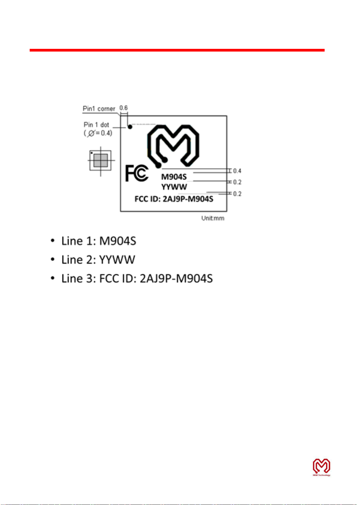
11.1 Product Marking ..................................................................................................... 24
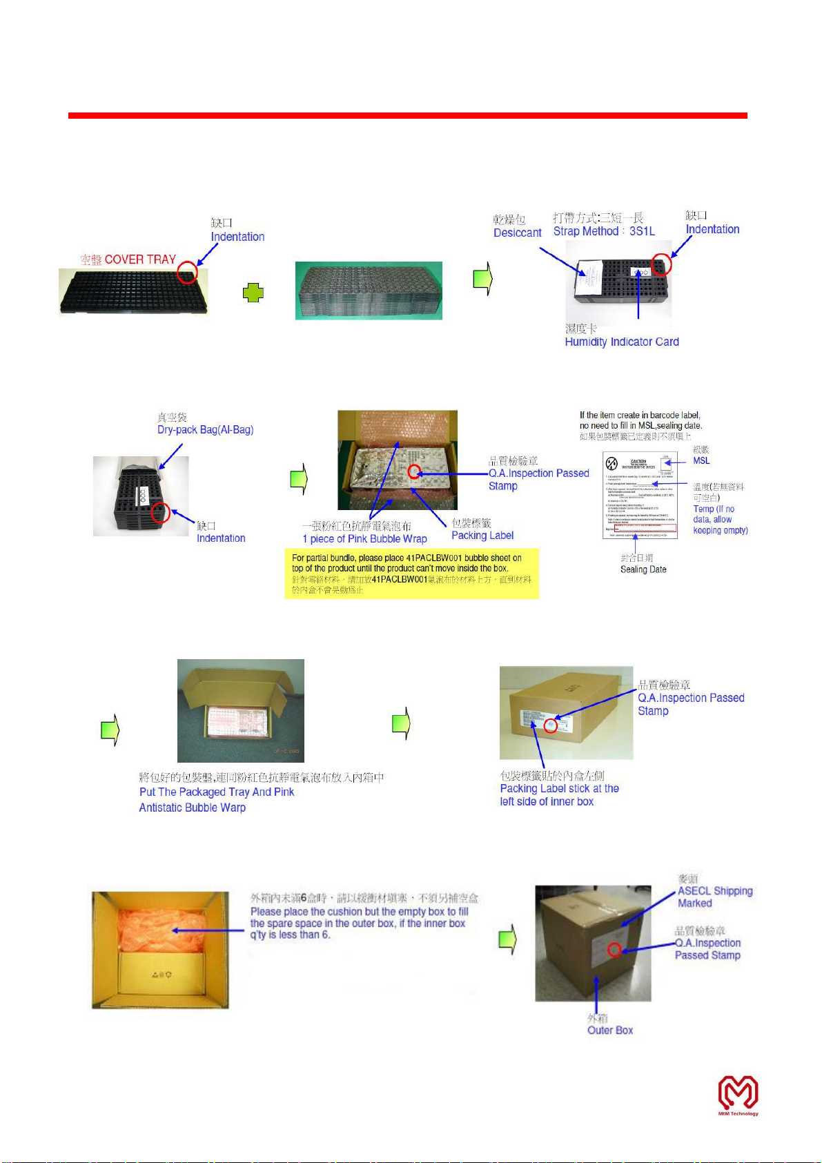
11.2 Package Information ............................................................................................... 25
12 BQB / CE/ FCC Certification .................................................................................. 26
© MtM Technology Corporation. All rights reserved.
Page 3 / 27
Page 4

MtM Technology Corporation
1 Description
The SiP module M904S is a small size module with conformal shielding.
The module provides full function of Bluetooth 4.0 Low Energy in a tiny
module via 48 pins LGA Foot Print. The M904S module provides
everything required to create Bluetooth 4.0 Low Energy product with RF,
baseband, MCU, qualified Bluetooth v4.0 stack and customer application
running on a single IC.
M904S enables ultra-low power connectivity and basic data transfer for
applications previously limited by the power consumption, size constraints
and complexity of other wireless standards. The low power consumption
and excellent radio performance make it the best solution for OEM /ODM
customers who require embedded Bluetooth 4.0 Low Energy feature, such
as, IP camera, car key, sport and fitness watch, mouse, led light bulb etc.
For the software and driver development, we provide extensive technical
document and reference software code for the system integration.
Hardware evaluation kit and development utilities will be released base on
listed OS and processors to OEM customers.
© MtM Technology Corporation. All rights reserved.
Page 4 / 27
Page 5
MtM Technology Corporation
Part Number
Description
M904S
CLASS 2 Bluetooth single mode Module according BT-4.0. Bluetooth SMART
2 Feature
Bluetooth® v4.0 LE radio technology
-90 dBm sensitivity in Bluetooth® low energy mode
250 kbps, 1 Mbps, 2 Mbps supported data rates
TX Power -20 to +4 dBm in 4 dB steps
TX Power -30 dBm Whisper mode
12 mA peak RX, 10 mA peak TX (0 dBm)
256 kB embedded flash program memory
Supply voltage range 1.8 V to 3.6 V
SPI Master/Slave
Low power comparator
Temperature sensor
Two-wire Master (I2C compatible)
UART (CTS/RTS)
AES HW encryption
Real Timer Counter (RTC)
Demo SW Open source on nRF51SDK v8/SoftDevice version 1
Supports the nRF51SDK v11/SoftDevice v2
LGA-48 package, 6.5 x 6.5 mm
ORDRING INFORMATION
© MtM Technology Corporation. All rights reserved.
Page 5 / 27
Page 6

MtM Technology Corporation
3 Block Diagram
M904S supports UART command line interface to connect to the host
processor. The simplified block diagram is depicted in the Fig. as below..
© MtM Technology Corporation. All rights reserved.
Page 6 / 27
Page 7
MtM Technology Corporation
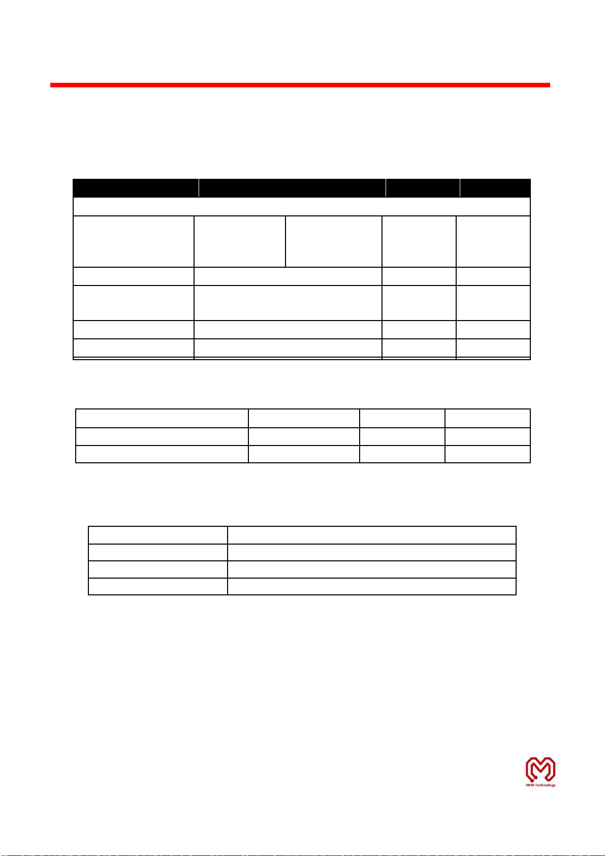
No
Description
Value
Unit
Ratings Over Operating Free-Air Temperature Range
1 Supply voltage
All supply pins
–0.3 to 3.9
V
must have the
same voltage
2 Voltage on any digital pin
TBD
V
3 Operating ambient temperature
–25 to 75
°C
range
4 Storage temperature range
–35 to 75
°C
5 Bluetooth RF output
4 ± 1
dBm
Operating Condition
Min.
Typ.
Max.
DVDD_3V3
1.8
3.3 3.6
I/O supply voltage (VDD_PADS)
1.2
3.3 3.6
Features
Description
Bluetooth Standards
Bluetooth core v4.0 Low Energy
Antenna Port
Support Single Antenna for Bluetooth
Frequency Band
2.402 – 2.480 GHz
4 Technical Specification
4.1 Recommendable Operation Condition
Temperature, humidity
The M904S module has to withstand the operational requirements as listed in the table below
4..2Voltage
Power supply for the M904S module will be provided by the host via the power pins
4.3 Wireless Specifications
The M904S module compliance with the following features and standards
© MtM Technology Corporation. All rights reserved.
Page 7 / 27
Page 8

MtM Technology Corporation
Features
Description
Frequency Band
2.402– 2.480 GHz (2.4 GHz ISM Band)
Number of selectable Sub channels
40 channels
Modulation
GFSK
Supported rates
<2Mbps
Maximum receive level
-10dBm (with PER <30. 8%)
Parameter
Mode and Conditions
Min.
Typ.
Max.
Unit.
RX sensitivity
-
-90
-
dBm
Maximum input
- -10
dBm
Frequency range
2400
-
2483
MHz
Output power adjustment
ranger
-20 - 4
dBm
Output power
- 2 -
dBm
Output power variation
- 4 -
dB
4.4 Radio Specifications Bluetooth 4.0 Low Energy
© MtM Technology Corporation. All rights reserved
Page 8 / 27
Page 9
MtM Technology Corporation
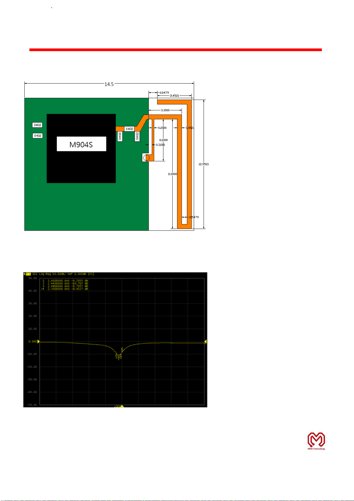
4.5 External Antenna Design Guide
4.5.1 PCB Antenna Design Guide: Peak Gain: -2dBi Typ. / Avg. Gain: -3.5dBi Typ. (XZ-V)
Return Loss
© MtM Technology Corporation. All rights reserved
Page 9 / 27
MtM Technology Corporation
Page 10
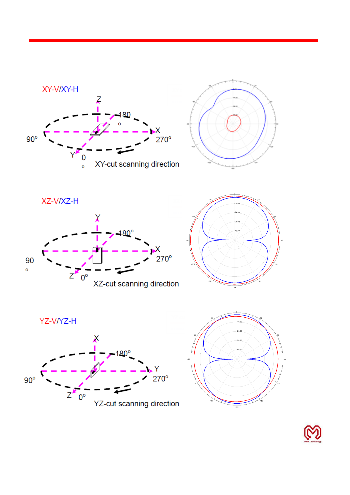
Radiation Patterns
© MtM Technology Corporation. All rights reserved
Page 10 / 27
MtM Technology Corporation
Page 11
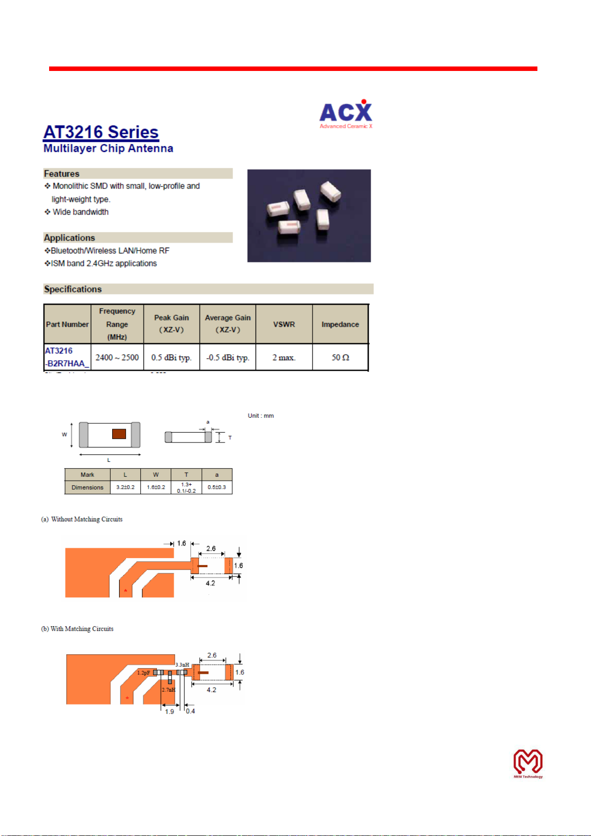
4.5.2 Chip Antenna Design Guide
Dimensions and Recommended PC Board Pattern
© MtM Technology Corporation. All rights reserved
Page11 / 27
MtM Technology Corporation
Page 12
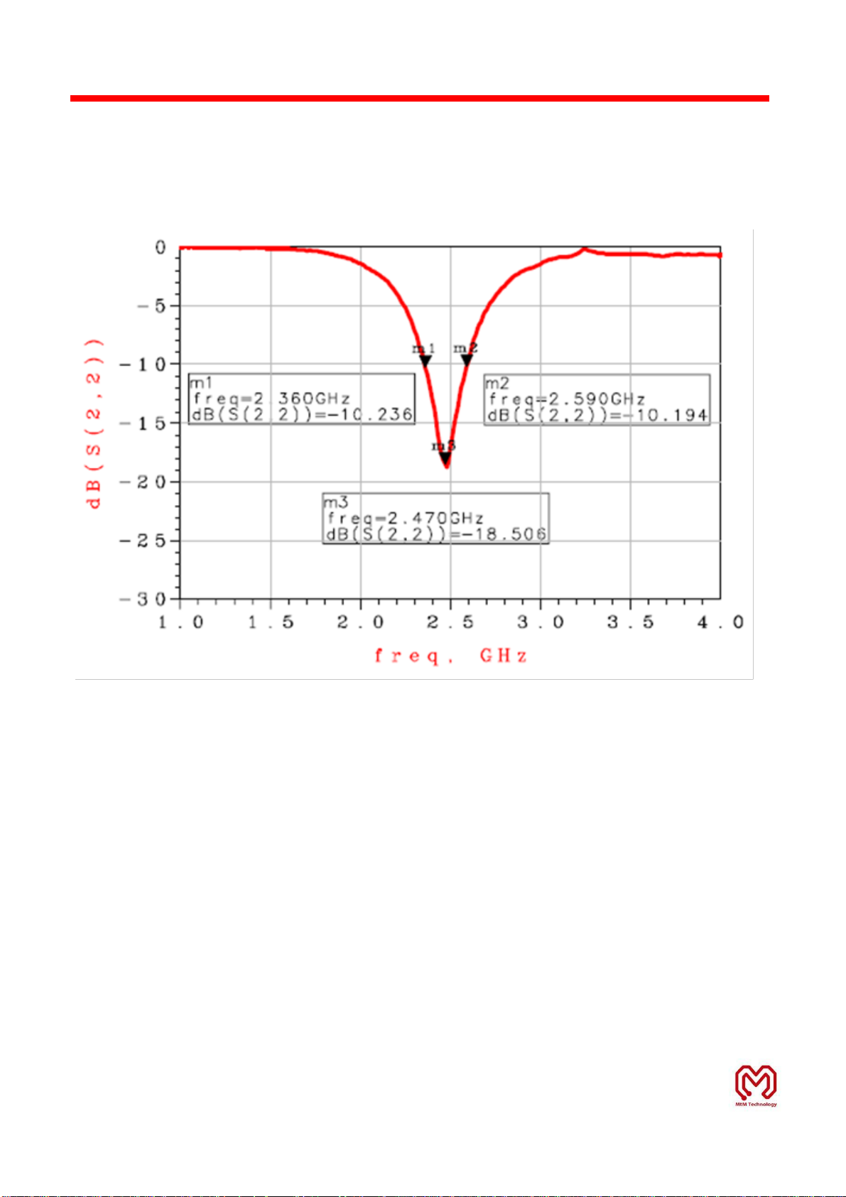
Return Loss\With Matching Circuits
© MtM Technology Corporation. All rights reserved
Page 12 / 27
Page 13
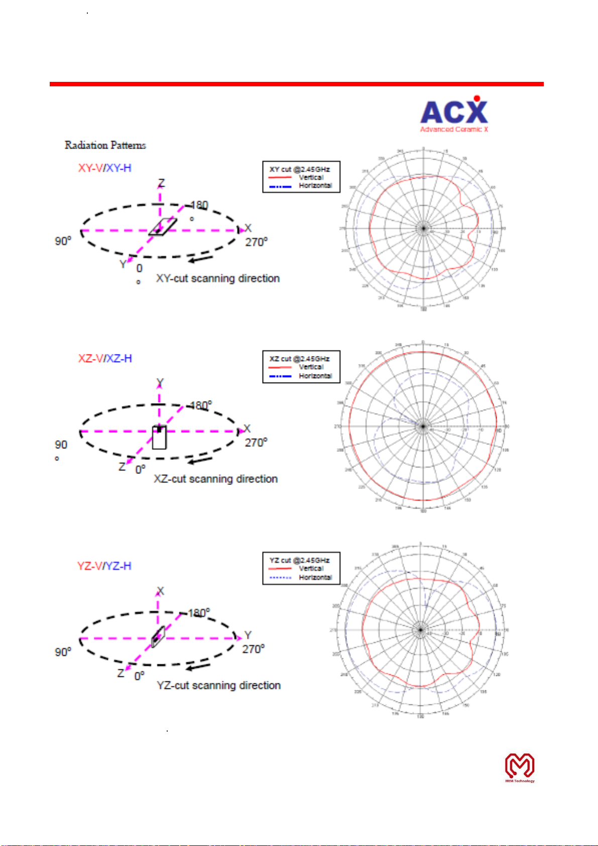
MtM Technology Corporation
© MtM Technology Corporation. All rights reserved
Page 13 / 27
Page 14
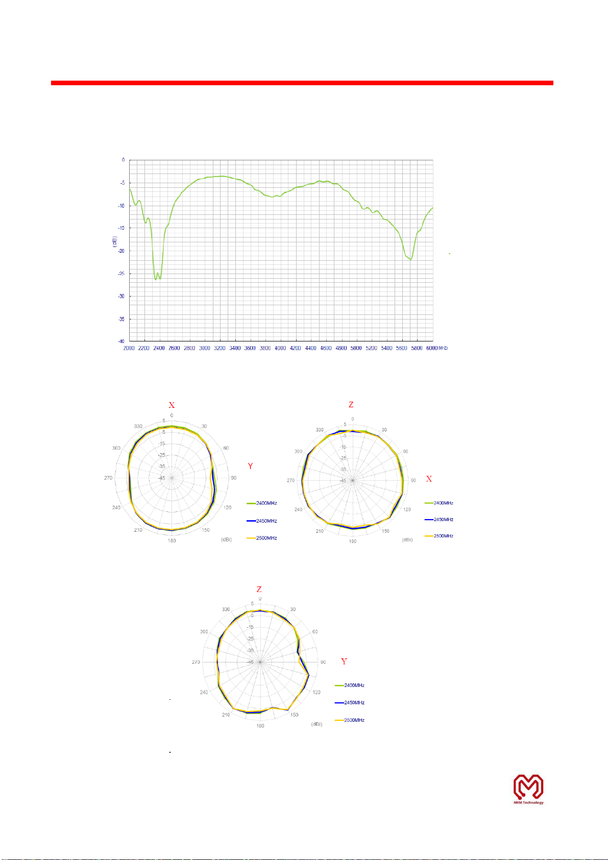
MtM Technology Corporation
4.5.2 Dipole Antenna Design Guide:
Return Loss
Radiation Patterns
xy-plane xz-plane
yz-plane
© MtM Technology Corporation. All rights reserved
Page 14 / 27
Page 15
MtM Technology Corporation
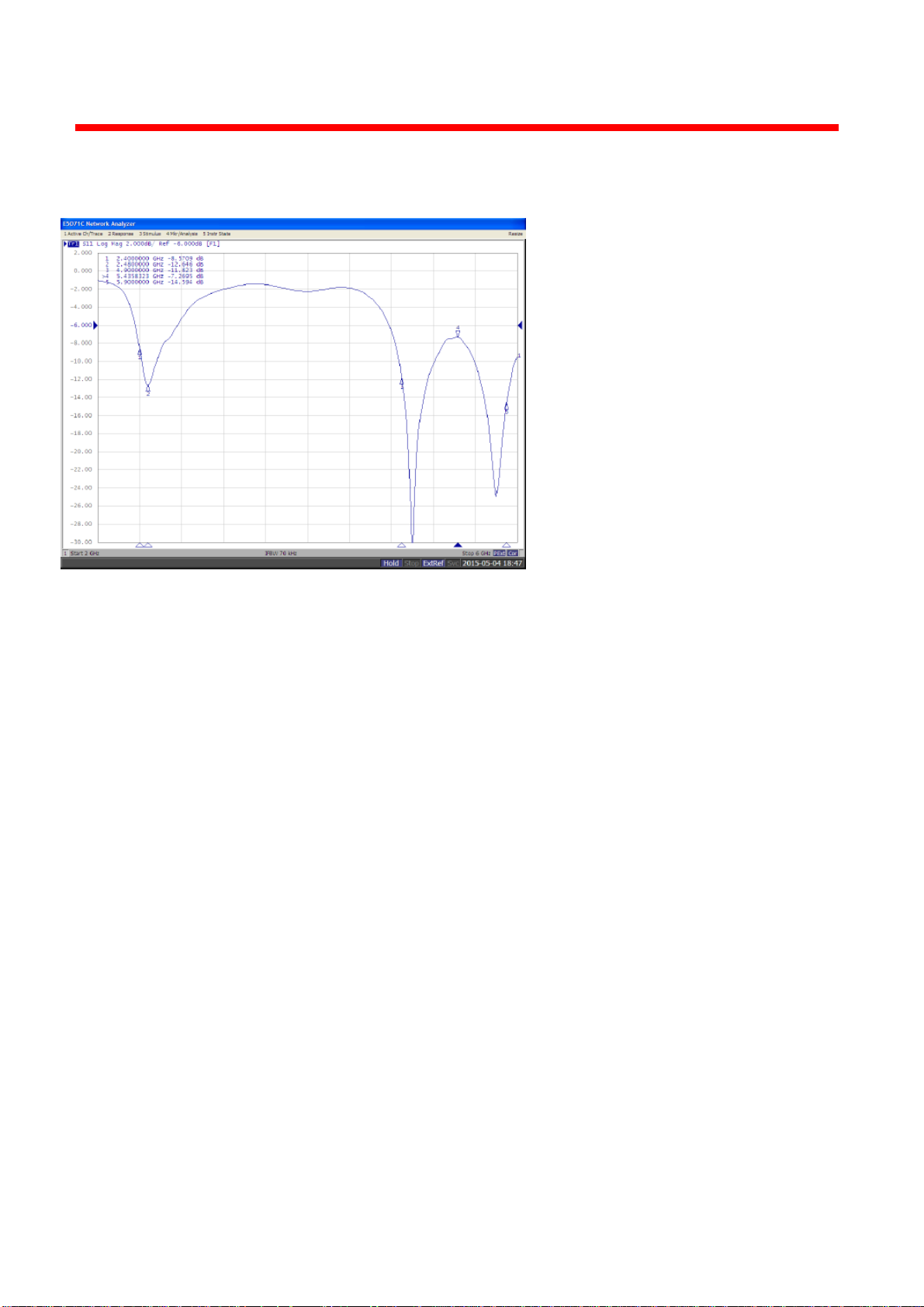
4.5.4 PIFA Antenna Design Guide:
Return Loss
Page 16
MtM Technology Corporation
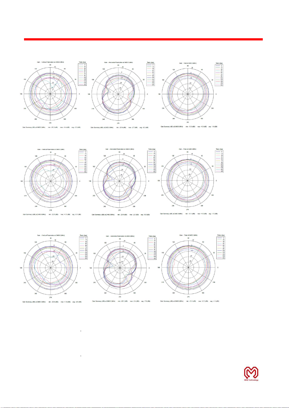
Radiation Patterns
Vertical, Horizontal and Total Gain Patterns at 2400MHz
Vertical, Horizontal and Total Gain Patterns at 2440MHz
Vertical, Horizontal and Total Gain Patterns at 2480MHz
© MtM Technology Corporation. All rights reserved
Page 14 / 27
Page 17
MtM Technology Corporation
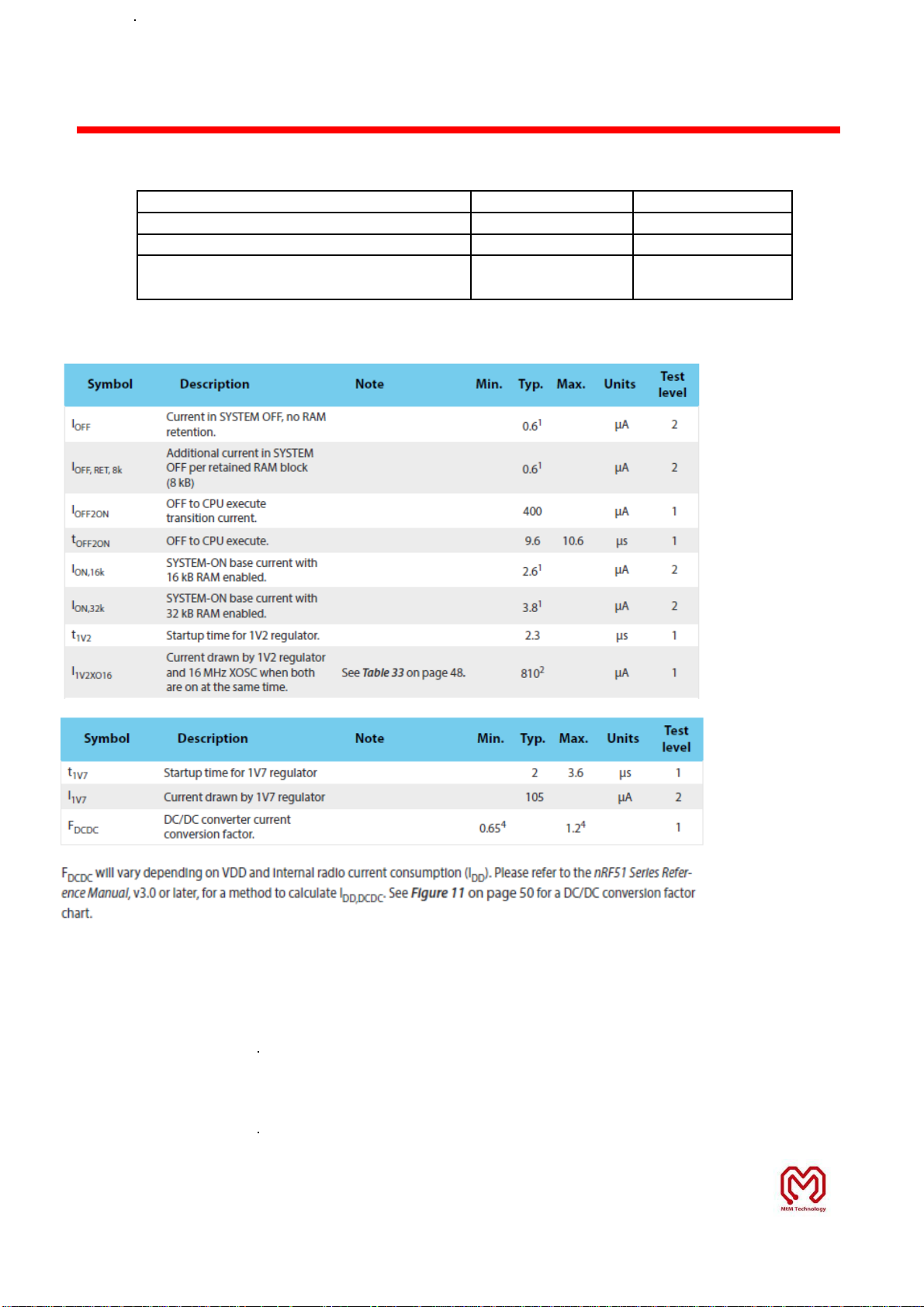
Item
Condition
Typ.
Tx mode
3.3V
9.76mA
Rx mode
3.3V
12.15mA
System ON
Constant Latency
Sleep Mode
0.41uA
4.6 Power Consumption
Power Management
© MtM Technology Corporation. All rights reserved
Page 14 / 27
Page 18
MtM Technology Corporation
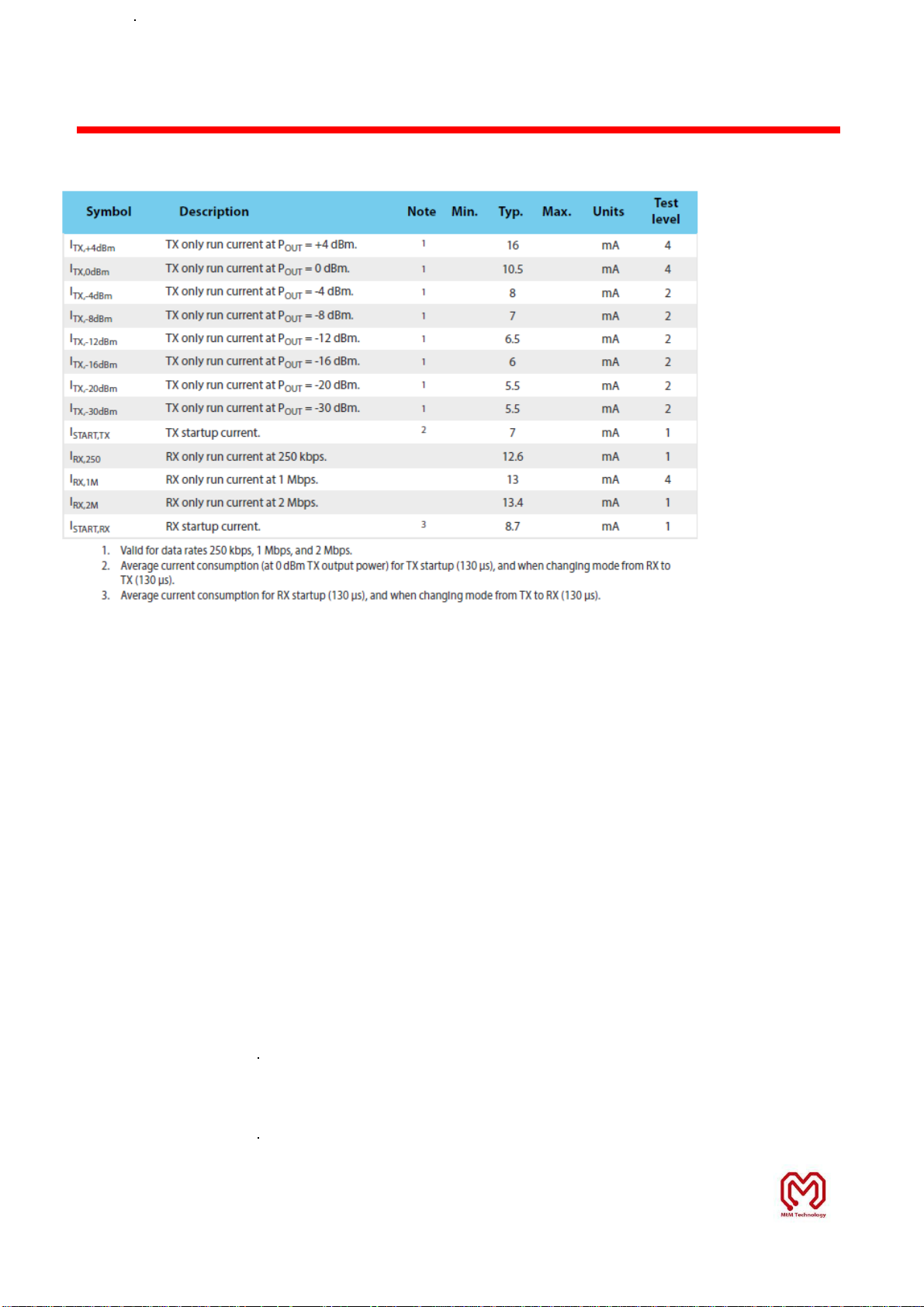
Radio Current Consumption
© MtM Technology Corporation. All rights reserved
Page 15 / 27
Page 19
MtM Technology Corporation
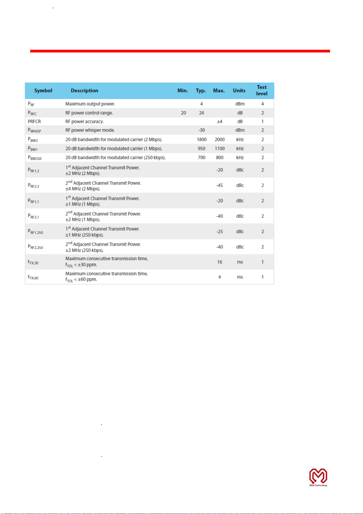
Transmitter Specifications
© MtM Technology Corporation. All rights reserved
Page 16 / 27
Page 20
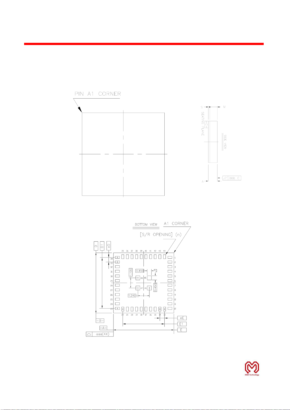
Top-View:
Side-View:
Bottom-View:
MtM Technology Corporation
5 Dimensions
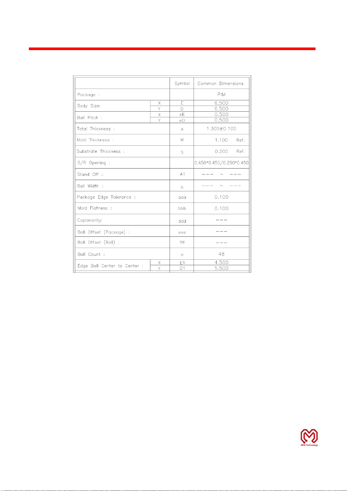
The size and thickness of the M904 module 6.5mm (W) x 6.5mm (L) x 1.3mm (H):
© MtM Technology Corporation. All rights reserved
Page 17 / 27
Page 21
MtM Technology Corporation
Dimensions
© MtM Technology Corporation. All rights reserved.
Page 18 / 27
Page 22
MtM Technology Corporation
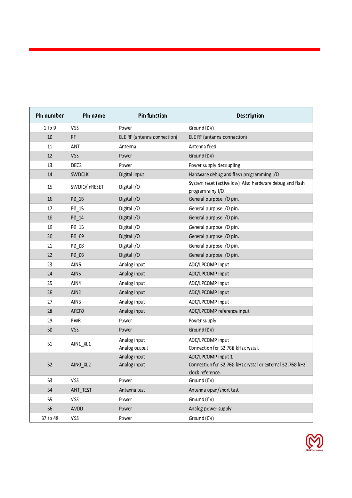
6 Pin Assignments
© MtM Technology Corporation. All rights reserved.
6.1Pin Description
The foot print dimension and pin definition is defined as below
Page 19 / 27
Page 23
MtM Technology Corporation
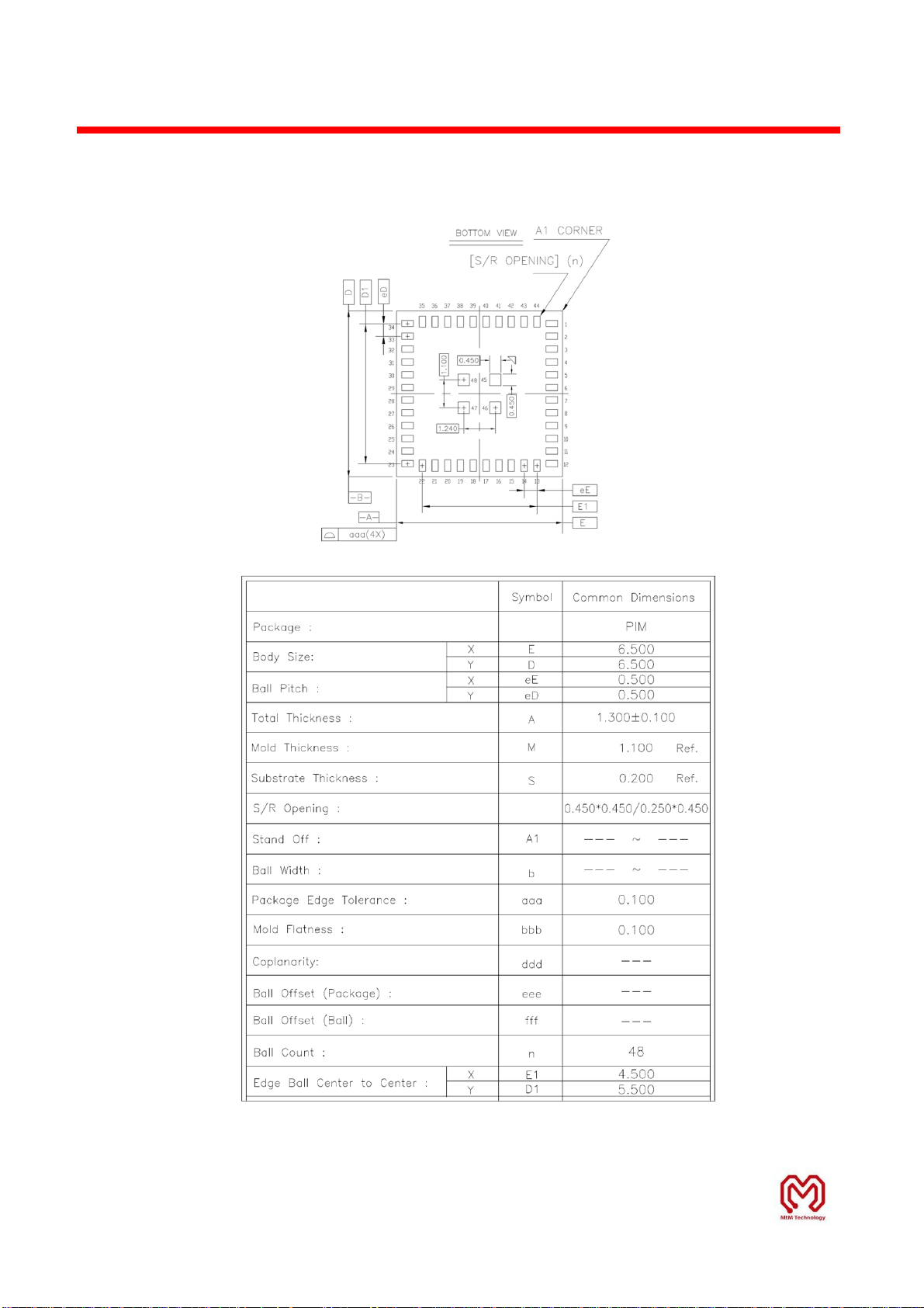
7 Recommend Footprint
Suggest on PCB: SMD (1:1)
© MtM Technology Corporation. All rights reserved.
Page 20 / 27
Page 24
MtM Technology Corporation
P0_27
P0_26
ANTU11
ANT
1
NC
2
2.4GHz Antenna
RF
50 Ohm trace
C2
1.0uF_0402
L6
N.L_0402
C9
0R_0402
L7
N.L_0402
VDD
AVDD
U1
M904S_BLE_Module
GND
1
GND
2
GND
3
GND
4
GND
5
GND
6
GND
7
GND
8
GND
9
RF
10
ANT
11
GND
12
DEC213SWDCLK14SWDIO_nRESET15P0_1616P0_1517P0_1418P0_1319P0_0920P0_0821P0_06_AIN7_AREF1
22
ANT_TEST
34
GND
33
P0_26_AIN0_XL2
32
P0_27_AIN1_XL1
31
GND
30
VDD
29
P0_00_AREF0
28
P0_02_AIN3
27
P0_01_AIN2
26
P0_03_AIN4
25
P0_04_AIN5
24
P0_05_AIN6
23
GND48GND47GND46GND45GND44GND43GND42GND41GND40GND39GND38GND
37
AVDD
36
GND
35
RF
P0_09
P0_08
P0_15
P0_14
P0_13
P0_16
C17 12PF_0402
Y1 NM_32.768kHz
C16 12PF_0402
C3
1.0uF_0402
RTC (External)
P0_00
P0_01
P0_02
P0_03
P0_05
P0_04
P0_06
SWDIO
SWDCLK
DEC2
P0_27
P0_26
DC Power
R5
0R_0402
R4
0R_0402
DEC2
VDD
AVDD
R2
0R_0402
R3
0R_0402
PWR
RTC
RF
JTAG
DEC
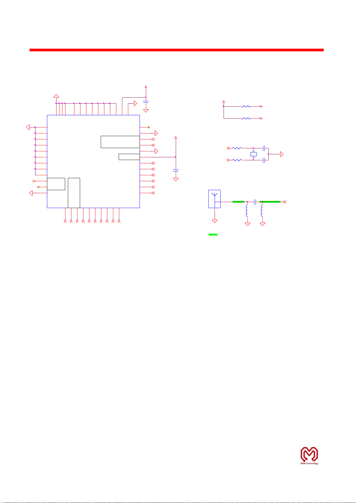
8 Reference Design Circuit
8.1 Reference Schematic
Page 21 / 27
© MtM Technology Corporation. All rights reserved.
Page 25
MtM Technology Corporation
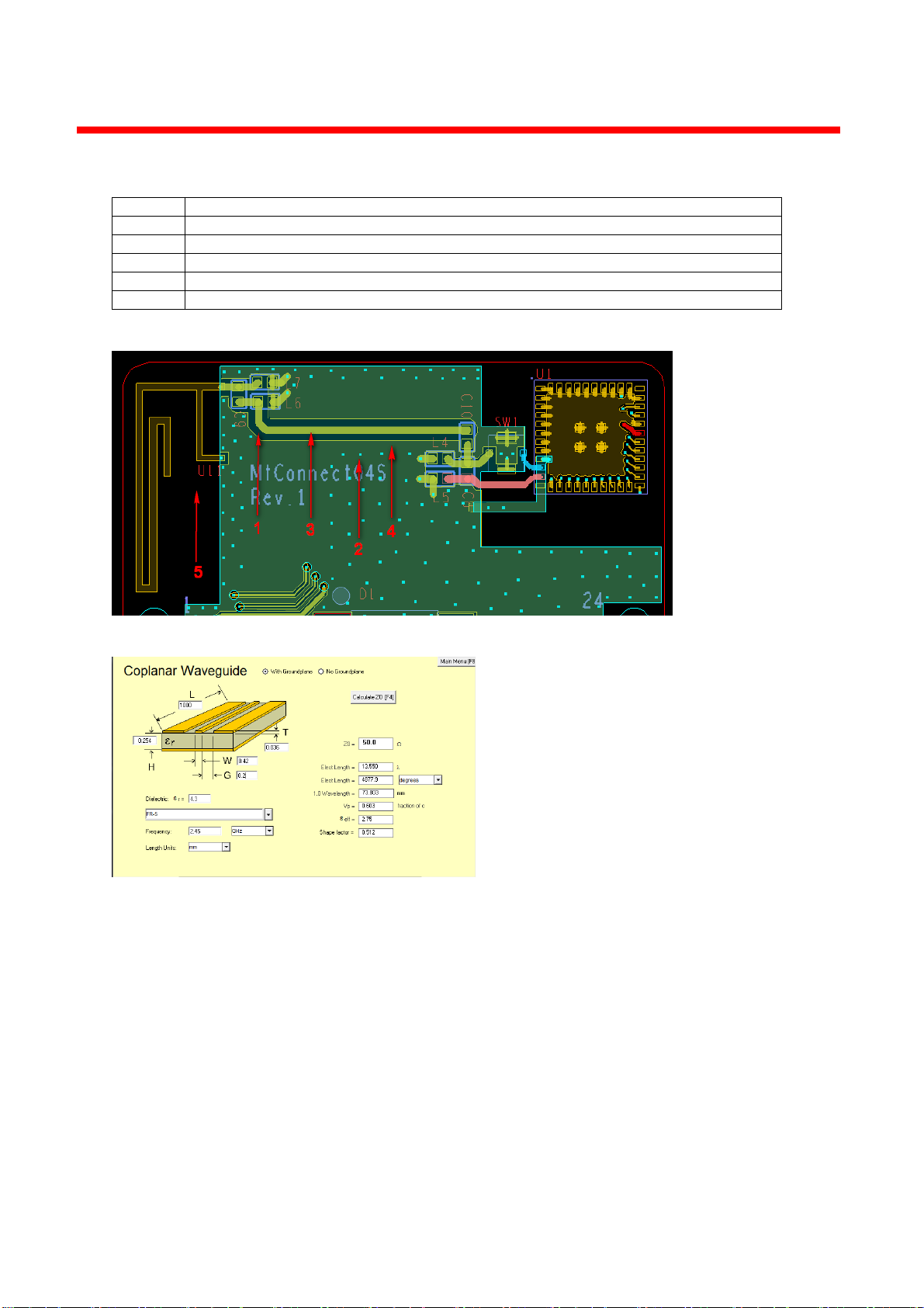
Re ference De s c rip t ion
1 Th e RF traces b e n d s must be g radu a l w ith an a p po x imate maxim u m bend of 4 5 degrees
2 RF trace s must have v ia on g ro u n d plan e besid e the RF tr a c e on b o th sid e s
3 RF trace s must have c o ns tant impedance (mic ro str ip t ransmissio n lin e )
4 RF trace g o u n d lay er must be the s o lid g ro u n d la y e r im m e d iate ly b elow RF tra c e .
5 Th e re m u s t b e n o tr ace an d g round under a n tenna s e c tio n
8.2 Layout Guide
The following points are observed for antenna.
RF Section Layout
RF Section Layout
CPW impedance Calculation
Page 26
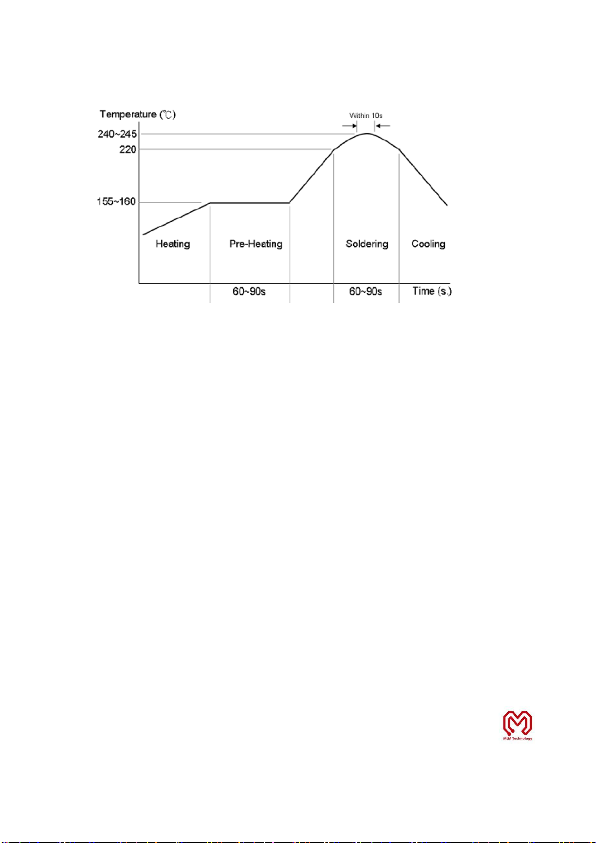
9 Recommended Reflow Profile
Profile Condition
© MtM Technology Corporation. All rights reserved.
a. Suitable for Lead-Free solder
b. Between 155~160°C: 60~90 sec.
c. Above 220°C: 60~90 sec.
d. Peak Temperature: 240~245 (<10 sec.)
Page 22 / 27
Page 27

MtM Technology Corporation
10 SiP Module Preparations
10.1 Handling
Handling the module must wear the anti-static wrist strap to avoid ESD damage. After each module
is aligned and tested, it should be transport and storage with anti-static tray and packing. This
protective package must be remained in suitable environment until the module is assembled and
soldered onto the main board.
10.2 SMT Preparation
1. Calculated shelf life in sealed bag: 6 months at <40℃ and <90% relative humidity (RH).
2. Peak package body temperature: 250℃.
3. After bag was opened, devices that will be subjected to reflow solder or other high temperature
process must.
A. Mounted within: 72 hours of factory conditions <30℃/60% RH.
B. Stored at ≦10% RH with N2 flow box.
4. Devices require baking, before mounting, if:
A. Package bag does not keep in vacuumed while first time open.
B. Humidity Indicator Card is >10% when read at 23±5℃.
C. Expose at 3A condition over 8 hours or Expose at 3B condition over 24 hours.
5. If baking is required, devices may be baked for 12 hours at 125±5℃.
© MtM Technology Corporation. All rights reserved.
Page 23 / 27
Page 28
MtM Technology Corporation
11 Package Information
11.1 Product Marking
© MtM Technology Corporation. All rights reserved.
Page 24 / 27
Page 29
MtM Technology Corporation
11.2 Package Information
----------------------------------------------------------------------------------------------------------------------------------------
----------------------------------------------------------------------------------------------------------------------------------------
----------------------------------------------------------------------------------------------------------------------------------------
© MtM Technology Corporation. All rights reserved.
Page 25 / 27
Page 30

MtM Technology Corporation
12 BQB/CE/FCC Certification
12.1 FCC (USA)
Federal Communication Commission Interference Statement
This equipment has been tested and found to comply with the limits for a Class B digital device,
pursuant to Part 15 of the FCC Rules. These limits are designed to provide reasonable protection
against harmful interference in a residential installation. This equipment generates, uses and can
radiate radio frequency energy and, if not installed and used in accordance with the instructions,
may cause harmful interference to radio communications. However, there is no guarantee that
interference will not occur in a particular installation. If this equipment does cause harmful
interference to radio or television reception, which can be determined by turning the equipment
off and on, the user is encouraged to try to correct the interference by one or more of the
following measures:
Reorient or relocate the receiving antenna.
Increase the separation between the equipment and receiver.
Connect the equipment into an outlet on a circuit different from that to which the receiver is
connected.
Consult the dealer or an experienced radio/TV technician for help.
FCC Caution: Any changes or modifications not expressly approved by the party responsible for
compliance could void the user's authority to operate this equipment.
This device complies with Part 15 of the FCC Rules. Operation is subject to the following two
conditions: (1) This device may not cause harmful interference, and (2) this device must accept
any interference received, including interference that may cause undesired operation.
This device and its antenna(s) must not be co-located or operating in conjunction with any other
antenna or transmitter.
IMPORTANT NOTE:
FCC Radiation Exposure Statement:
This equipment complies with FCC radiation exposure limits set forth for an uncontrolled
environment. This equipment should be installed and operated with minimum distance 20cm
between the radiator & your body.
© MtM Technology Corporation. All rights reserved.
Page 26 / 27
Page 31

IMPORTANT NOTE:
This module is intended for OEM integrator.
The OEM integrator is still responsible for the FCC compliance requirement of the end product,
which integrates this module.
Appropriate measurements (e.g. 15 B compliance) and if applicable additional equipment
authorizations (e.g. Verification , Doc) of the host device to be addressed by the
integrator/manufacturer.
IMPORTANT NOTE:
This module is intended for OEM integrator. The OEM integrator is still responsible for the FCC
compliance requirement of the end product, which integrates this module.
20cm minimum distance has to be able to be maintained between the antenna and the users for
the host this module is integrated into. Under such configuration, the FCC radiation exposure
limits set forth for an population/uncontrolled environment can be satisfied.
Any changes or modifications not expressly approved by the manufacturer could void the user's
authority to operate this equipment.
USERS MANUAL OF THE END PRODUCT:
In the users manual of the end product, the end user has to be informed to keep at least 20cm
separation with the antenna while this end product is installed and operated. The end user has to
be informed that the FCC radio-frequency exposure guidelines for an uncontrolled environment
can be satisfied. The end user has to also be informed that any changes or modifications not
expressly approved by the manufacturer could void the user's authority to operate this equipment.
If the size of the end product is smaller than the palm of the hand, then additional FCC part 15.19
statement is required to be available in the users manual: This device complies with Part 15 of
FCC rules. Operation is subject to the following two conditions: (1) this device may not cause
harmful interference and (2) this device must accept any interference received, including
interference that may cause undesired operation.
LABEL OF THE END PRODUCT:
The final end product must be labeled in a visible area with the following " Contains TX FCC ID:
2AJ9P-M904S". If the size of the end product is larger than the palm of the hand, then the
following FCC part 15.19 statement has to also be available on the label: This device complies
with Part 15 of FCC rules. Operation is subject to the following two conditions: (1) this device
may not cause harmful interference and (2) this device must accept any interference received,
including interference that may cause undesired operation.
Professional installation
Section 15.204(b) states that an approved "transmission system" must always be marketed as a
complete system including the antenna.
© MtM Technology Corporation. All rights reserved.
Page 27 / 27
 Loading...