

Page 1
INSTRUCTION MANUAL
MODBUS INTERFACE MODULE
(For temperature control module)
BEFORE USE ....
Thank you for choosing M-System. Before use, please check
contents of the package you received as outlined below.
If you have any problems or questions with the product,
please contact M-System’s Sales Office or representatives.
■ PACKAGE INCLUDES:
Network interface module ..................................................(1)
Terminating resistor (110 Ω, 0.25 W) .................................(1)
■ MODEL NO.
Confirm Model No. marking on the product to be exactly
what you ordered.
■ INSTRUCTION MANUAL
This manual describes necessary points of caution when
you use this product, including installation, connection and
basic maintenance procedures.
POINTS OF CAUTION
■ HOT INSERTION/REMOVAL OF MODULES
• It is possible to replace the module with the power is supplied. Be sure to replace it when the module is not communicating with a host, as it is possible to affect the system. However, replacing multiple modules at once may
greatly change line voltage levels. We recommend that
you replace them one by one.
MODEL
■ AND ....
• The unit is designed to function as soon as power is supplied, however, a warm up for 10 minutes is required for
satisfying complete performance described in the data
sheet.
R3-NM3
INSTALLATION
Use the Installation Base Model R3-BS, or Model R3-BSW
for free I/O address capability.
Before mounting the Network Interface Module onto the
Base, be sure to configure the module as explained below.
■ DATA ALLOCATION
The setting determines the data area size assigned to each
I/O module mounted on the base.
The data sent/received via Modbus is mapped according to
this setting.
See “COMPONENT IDENTIFICATION” and “MODBUS
I/O ASSIGNMENTS”.
■ NODE ADDRESS & BAUD RATE, ETC.
See “COMPONENT IDENTIFICATION”.
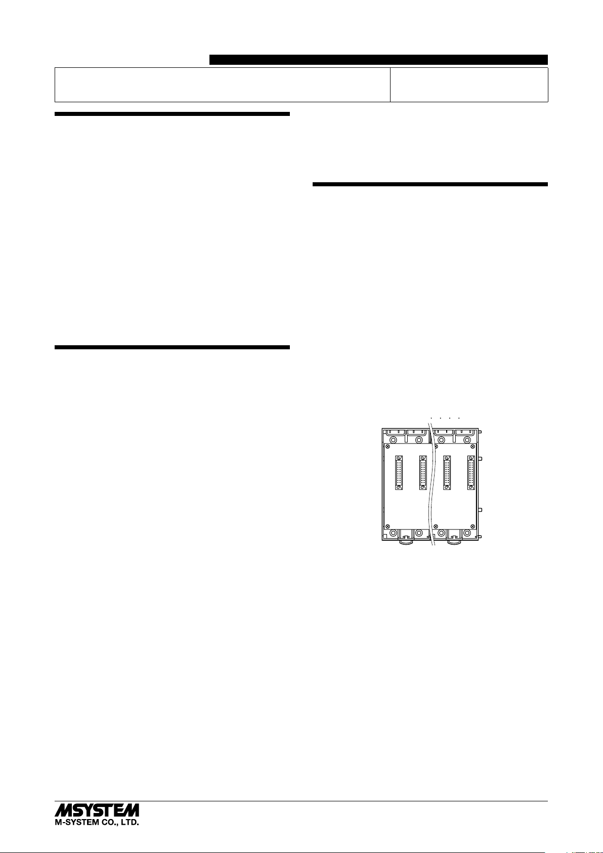
■ NETWORK SLOTS ON THE BASE
I/O 1 I/O 2 I/O n
■ POWER INPUT RATING & OPERATIONAL RANGE
• Locate the power input rating marked on the product and
confirm its operational range as indicated below:
100 – 120V AC rating: 85 – 132V, 47 – 66 Hz, approx. 20VA
200 – 240V AC rating: 170 – 264V, 47 – 66 Hz, approx. 20VA
24V DC rating: 24V ±10%, approx. 12W
■ GENERAL PRECAUTIONS
• DO NOT set the switches on the module while the power
is supplied. The switches are used only for maintenance
without the power.
■ ENVIRONMENT
• Indoor use.
• When heavy dust or metal particles are present in the
air, install the unit inside proper housing with sufficient
ventilation.
• Do not install the unit where it is subjected to continuous
vibration. Do not subject the unit to physical impact.
• Environmental temperature must be within -10 to +55°C
(14 to 131°F) with relative humidity within 30 to 90% RH
in order to ensure adequate life span and operation.
■ WIRING
• Do not install cables close to noise sources (relay drive
cable, high frequency line, etc.).
• Do not bind these cables together with those in which
noises are present. Do not install them in the same duct.
With Model R3-BS base, mount the I/O Modules from the
left end (I/O 1) to the right in order that the Network Module assigns data areas from I/O 1.
Network Module(s) and Power Module are mounted basically at the right end though technically they could be
mounted in any position.
With Model R3-BSW base, there is no limitation in mounting positions as I/O address can be assigned freely to each
module using rotary switches equipped on the base.
5-2-55, Minamitsumori, Nishinari-ku, Osaka 557-0063 JAPAN
Phone: +81(6)6659-8201 Fax: +81(6)6659-8510 E-mail: info@m-system.co.jp
EM-8330 Rev.3 P. 1 / 9
Page 2
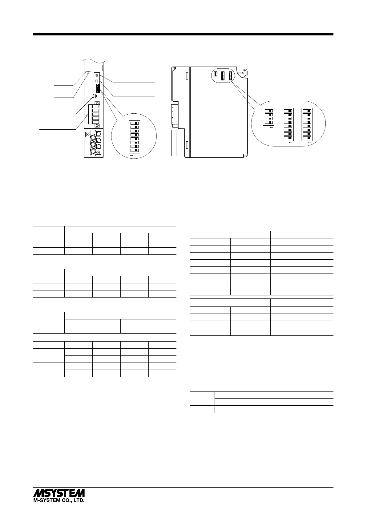
COMPONENT IDENTIFICATION
■ FRONT VIEW ■ SIDE VIEW
D
C
E
B
F
A
9
0
8
1
7
2
SA1
3
6
5
4
D
C
E
B
F
A
Node Address (MSD)
9
0
8
1
7
SA2
2
3
6
5
RUN LED
4
R3-NM3
ERR LED
Configuration Jack
Euro Type
Connector Terminal
4
5
6
Node Address (LSD)
FG
SLD
DG
DB
DA
1
2
3
DIP SW
SW6
8
7
6
5
4
3
2
1
ON
■ FRONT ROTARY SW
• Node Address: SA1, SA2
Set the module’s node address in hexadecimal with SA1 and
SA2. (Setpoint adjustment: 01 – F7)
■ FRONT DIP SW
(*) Factory setting
• Baud Rate: SW6-1, 6-2
SW
38.4k (*) 19.2k 9600
BAUD RATE (bps)
4800
SW6-1 OFF ON OFF ON
SW6-2 OFF OFF ON ON
• Parity: SW6-3, 6-4*
SW
1
PARITY
NONE (*) ODD EVEN
N/A
SW6-3 OFF ON OFF ON
SW6-4 OFF OFF ON ON
• Data Mode: SW6-5*
SW
1
DATA MODE
RTU (Binary) ASCII
SW6-5 OFF ON
*1. Bit assignment according to Parity and Data Mode setting.
MODE STA RT DATA PARITY STOP
RTU
ASCII
1 8 1 1
1 8 None 2
1 7 1 1
1 7 None 2
Note: Be sure to set unused SW6-6 through 6-8 to OFF.
DIP SW
SW3
4
3
2
1
ON
SW2
8
7
6
5
4
3
2
1
ON
SW1
8
7
6
5
4
3
2
1
ON
■ SIDE DIP SW
(*) Factory setting
• Data Allocation: SW1, SW2
2
Data Allocation Type*
must be assigned to each I/O module
slot position to specify how many data areas (four types) are
to be occupied by each.
Two bits from SW1 and SW2 are assigned to each position,
and data areas can be specified from the slot No. 1 through
8. Setting for No. 9 and later slots is identical to No. 8.
SW ASSIGNMENT SLOT
SW1-1 SW1-2 1
SW1-3 SW1-4 2
SW1-5 SW1-6 3
SW1-7 SW1-8 4
SW2-1 SW2-2 5
SW2-3 SW2-4 6
SW2-5 SW2-6 7
SW2-7 SW2-8 8
SW SETTING DATA ALLOCATION
OFF OFF 1
ON OFF 4
OFF ON 8
ON ON 16
*2. Refer to the specifications of the related series for the Data
Allocation Type of I/O modules.
• Dual Communication: SW3-1
When two network modules are mounted, one must be
‘Main’ (OFF) network and the other must be ‘Sub’ (ON) network. For single communication, the network module must
always be set to ‘Main’ (OFF).
SW
DUAL COMMUNICATION
MAIN (*)
SUB
SW3-1 OFF ON
5-2-55, Minamitsumori, Nishinari-ku, Osaka 557-0063 JAPAN
Phone: +81(6)6659-8201 Fax: +81(6)6659-8510 E-mail: info@m-system.co.jp
EM-8330 Rev.3 P. 2 / 9
Page 3
• Input Error Data: SW3-2
Hold: When the communication from an input module is lost
due to the input module error, the network module holds the
signal and stands by until the communication recovers.
Set to ‘0’: When the communication from an input module
is lost due to the input module error, the network module
outputs ‘0.’
SW
SW3-2 OFF ON
INPUT ERROR DATA
HOLD (*)
SET ‘0’
• Main/Sub Switching Control: SW3-3
The host PC or PLC can choose whether ‘Main’ or ‘Sub’ bus
is used when the switching control is set to ‘Host.’
In ‘Normal’ mode, ‘Main’ bus is normally used, while ‘Sub’
bus is when the main communication has failed.
Be sure to match this control mode for both network modules in dual communication mode.
SW
SW3-3 OFF ON
Note: Set SW3-3 to OFF for use in single communication mode.
MAIN/SUB SWITCHING CONTROL
NORMAL (*)
HOST
• LED Function: SW3-4
Functions assigned to the front RUN and ERR LEDs can
be selected.
SW3-4
OFF (*) Green when normal Green when abnormal
ON Red when receiving Red when transmitting
LED FUNCTION
RUN ERR
R3-NM3
PC CONFIGURATOR
With configurator software, settings shown below are available.
Refer to the software manual of R3CON for detailed operation.
■ NETWORK MODULE SETTING
PARAMETER AVAILABLE RANGE DEFAULT SETTING
Time (no communication time) 0.2 – 3200.0 (sec.) 3.0 (sec.)
5-2-55, Minamitsumori, Nishinari-ku, Osaka 557-0063 JAPAN
Phone: +81(6)6659-8201 Fax: +81(6)6659-8510 E-mail: info@m-system.co.jp
EM-8330 Rev.3 P. 3 / 9
Page 4

TERMINAL CONNECTIONS
Connect the unit as in the diagram below.
■ EXTERNAL DIMENSIONS unit: mm (inch)
27.5 (1.08)
130 (5.12)
1
4
2
5
3
6
■ CONNECTION DIAGRAM
FG
RUN +
RUN –
U (+)
V (–)
*
FG
SLD
DG
DB
DA
1
4
2
3
6
JACK
To Other
Modbus
Devices
RUN CONTACT OUTPUT
*
POWER INPUT
CONFIGURATION JACK
6–M3
SCREW
6.2
(.24)
TERMINAL
COVER
INTERNAL BUS
INTERNAL
POWER
BUS CONNECTOR
R3-NM3
109 (4.29)
POSITIONING
GUIDE
WIRING INSTRUCTIONS
■ M3 SCREW TERMINAL (power input, RUN contact output)
Torque: 0.5 N·m
■ SOLDERLESS TERMINAL
Refer to the drawing below for recommended ring tongue
terminal size. Spade tongue type is also applicable. Solderless terminals with insulation sleeve do not fit.
Recommended manufacturer: Japan Solderless Terminal
MFG.Co.Ltd, Nichifu Co.,ltd
Applicable wire size: 0.75 to 1.25 mm
3max
4min
2
3.2 dia.
*Not provided with ‘No Power Supply’ type module.
Caution: FG terminal is NOT a protective conductor terminal.
COMMUNICATION CABLE CONNECTIONS
TERMINATOR
HOST PC
Tx+ / Rx+
Tx– / Rx–
SG
Rx+
Rx–
5-2-55, Minamitsumori, Nishinari-ku, Osaka 557-0063 JAPAN
Phone: +81(6)6659-8201 Fax: +81(6)6659-8510 E-mail: info@m-system.co.jp
6max
12max
■ EURO TYPE CONNECTOR TERMINAL (Modbus)
Applicable wire size: 0.2 to 2.5 mm
Stripped length: 7 mm
MODBUS
INTERFACE
MODULE
DA
DB
DG
SLD
FG
FG
FG
(mm)
2
(AWG24 to 12)
MODBUS
INTERFACE
MODULE
DA
DB
DG
SLD
FG
EM-8330 Rev.3 P. 4 / 9
Page 5

R3-NM3
MODBUS FUNCTION CODES & SUPPORTED CODES
■ Data and Control Functions
CODE NAME
01 Read Coil Status X Digital output from the slave
02 Read Input Status X Status of digital inputs to the slave
03 Read Holding Registers X General purpose register within the slave
04 Read Input Registers X Collected data from the field by the slave
05 Force Single Coil X Digital output from the slave
06 Preset Single Registers X General purpose register within the slave
07 Read Exception Status
08 Diagnostics X
09 Program 484
10 Poll 484
11 Fetch Comm. Event Counter X Fetch a status word and an event counter
12 Fetch Comm. Event Log X A status word, an event counter, a message count and a field of event bytes
13 Program Controller
14 Poll Controller
15 Force Multiple Coils X Digital output from the slave
16 Preset Multiple Registers X General purpose register within the slave
17 Report Slave ID X Slave type / ‘RUN’ status
18 Program 884/M84
19 Reset Comm. Link
20 Read General Reference
21 Write General Reference
22 Mask Write 4X Register
23 Read/Write 4X Register
24 Read FIFO Queue
■ Exception Codes
CODE NAME
01 Illegal Function
02 Illegal Data Address
03 Illegal Data Value
X
Function code is not allowable for the slave
X
Address is not available within the slave
X
Data is not valid for the function
04 Slave Device Failure
05 Acknowledge
06 Slave Device Busy
07 Negative Acknowledge
08 Memory Parity Error
■ Diagnostic Subfunctions
CODE NAME
00 Return Query Data X Loop back test
01 Restart Comm. Option X Reset the slave and clear all counters
02 Return Diagnostic Register X Contents of the diagnostic data (2 bytes)
03 Change ASCII Input Delimiter X Delimiter character of ASCII message
04 Force Listen Only Mode X Force the slave into Listen Only Mode
5-2-55, Minamitsumori, Nishinari-ku, Osaka 557-0063 JAPAN
Phone: +81(6)6659-8201 Fax: +81(6)6659-8510 E-mail: info@m-system.co.jp
EM-8330 Rev.3 P. 5 / 9
Page 6

R3-NM3
MODBUS I/O ASSIGNMENTS
ADDRESS DATA FORMAT NAME
Coil (0X) 1 – 1024 Digital Output (discrete output)
1025 Main / Sub Switching Command (valid only with SW3-3 set to ON)
Inputs (1X) 1 – 1024 Digital Input (discrete input)
1025 – 1040 Module Status
1041 – 1056 Error Status
1057 – 1072 Data Error Status
Input Registers (3X) 1 – 256 I Analog Input
257 – 768 F Analog Input
Holding Registers (4X) 1 – 256 I Analog Output
257 – 768 F Analog Output
2001 – 50000 Extended I/O
I: Integer, 0 – 10000 (0 – 100%)
F: Floating (32-bit data cannot be accessed using floating addresses.)
Note: DO NOT access addresses other than mentioned above. Such access may cause problems such as inadequate operation.
• Module Status indicates whether individual I/O module are mounted or not. The bit corresponding to the mounted slots
turns to “1,” and the unmounted slots to “0.”
• Error Status indicates error status for each module as described below. The bit corresponding to such modules turns to “1.”
R3-TSx, R3-RSx, R3-US4: Input burnout
R3-DA16A: Power input in error or disconnected
R3-YSx: Output current error (e.g. load unconnected)
• Data Error Status indicates overrange (R3-US4: out of -10% to +110%; the other types: out of -15% to +115%) status for each
module. The bit corresponding to such modules turns to “1.”
• Main / Sub Switching Commands given to the network modules result as follows:
‘MAIN’ MODULE ‘SUB’ MODULE OUTPUT MODE
1 0 Main bus is used; Red light turns on at RUN LED of the I/O modules.
0 1 Sub bus is used; Green light turns on at RUN LED of the I/O modules.
1 1 Main bus is used; Amber light turns on at RUN LED of the I/O modules.
0 0 Output is invalid; RUN LED of the I/O modules turns off.
• In the extended I/O area, 3000 words are mapped for each I/O module.
Refer to the instruction manual of each I/O module for details.
SLOT ADDRESS
1 2001 – 5000
2 5001 – 8000
3 8001 – 11000
4 11001 – 14000
: :
14 44001 – 47000
15 47001 – 50000
5-2-55, Minamitsumori, Nishinari-ku, Osaka 557-0063 JAPAN
Phone: +81(6)6659-8201 Fax: +81(6)6659-8510 E-mail: info@m-system.co.jp
EM-8330 Rev.3 P. 6 / 9
Page 7

R3-NM3
TRANSMISSION DATA ASSIGNMENTS
DIP SW located at the side of the module specifies each I/O module’s data allocation (occupied data area).
For example, when the data areas are assigned as shown below:
Module 1 4
Module 2 4
Module 3 4
Module 4 1
Module 5 1
Module 6 1
Module 7 1
Then the I/O data are assigned as in the table below:
ADDRESS POSITION ADDRESS POSITION
Input Registers (3X)
Holding Registers (4X)
For Coil (0X) and Inputs (1X), addresses 16 times assigned data areas (Data Allocation Type) are allotted with the Data Allocation Type ‘1’ and ‘4.’ With ‘8’ and ‘16,’ 64 (4 × 16) are automatically assigned.
1 – 4, 257 – 264 Slot 1 Coil (0X)
5 – 8, 265 – 272 Slot 2 65 – 128 Slot 2
9 – 12, 273 – 280 Slot 3 129 – 192 Slot 3
13, 281 – 282 Slot 4 193 – 208 Slot 4
14, 283 – 284 Slot 5 209 – 224 Slot 5
15, 285 – 286 Slot 6 225 – 240 Slot 6
16, 287 – 288 Slot 7 241 – 256 Slot 7
Inputs (1X)
1 – 64 Slot 1
MODULE STATUS, ERROR STATUS, DATA ERROR STATUS
Shows each module’s availability and error status.
15
0
Module 1
Module 2
Module 3
:
Module 16
I/O DATA DESCRIPTIONS
The data allocations for typical I/O modules are shown below.
Refer to the manual for each module for detailed data allocations.
■ ANALOG DATA (16-bit data, models: R3-SV4, YV4, DS4, YS4 and US4, etc.)
16-bit binary data.
Basically, 0 to 100% of the selected I/O range is converted into 0 to 10000 (binary). Negative percentage is represented in 2’s
complements.
15
■ TEMPERATURE DATA (16-bit data, models: R3-RS4, TS4 and US4, etc.)
16-bit binary data.
With °C temperature unit, raw data is multiplied by 10. For example, 25.5°C is converted into 255.
With °F temperature unit, the integer section of raw data is directly converted into the data. For example, 135.4°F is converted into 135.
Minus temperature is converted into negative values, represented in 2’s complements.
0
15
5-2-55, Minamitsumori, Nishinari-ku, Osaka 557-0063 JAPAN
Phone: +81(6)6659-8201 Fax: +81(6)6659-8510 E-mail: info@m-system.co.jp
0
EM-8330 Rev.3 P. 7 / 9
Page 8

R3-NM3
1 : ON
■ ANALOG DATA (16-bit data, models: R3-CT4A, CT4B, etc.)
16-bit binary data.
Integer that engineering unit value (A) multiplied by 100 (for CLSE-R5, integer that engineering unit value (A) multiplied
by 1000).
15
0
■ ACCUMULATED COUNT DATA (32-bit data, models: R3-PA2, PA4A, WT1, WT4, etc.)
32-bit binary data is used for accumulated counts and encoder positions.
Lower 16 bits are allocated from the lowest address to higher ones, higher 16 bits in turn.
32-bit data cannot be accessed using floating addresses.
15
+0
15
+1
0
Lower 16 bits
0
Higher 16 bits
■ BCD DATA (32-bit data, models: R3-BA32A, BC32A, etc.)
32-bit binary data is used for BCD.
Lower 16 bits are allocated from the lowest address to higher ones, higher 16 bits in turn.
32-bit data cannot be accessed using floating addresses.
15
+0
15
+1
0
Lower 16 bits
0
Higher 16 bits
■ DISCRETE DATA (models: R3-DA16 and DC16, etc.)
15
0 : OFF
■ TEMPERATURE CONTROL DATA (model: R3-TC2)
Refer to the instruction manual of the R3-TC2.
0
Input 1 (Output 1)
Input 2 (Output 2)
Input 3 (Output 3)
: :
Input 16 (Output 16)
5-2-55, Minamitsumori, Nishinari-ku, Osaka 557-0063 JAPAN
Phone: +81(6)6659-8201 Fax: +81(6)6659-8510 E-mail: info@m-system.co.jp
EM-8330 Rev.3 P. 8 / 9
Page 9

■ MAIN / SUB SWITCHING CONTROL
R3 main network
(main/sub switching control)
Address : 01025 = 1
Address : 01025 = 0
R3-NM3
Communication Status Start Main Lost Main Restored Switching by Host
R3 sub network
(main/sub switching control)
Address : 01025 = 1
Address : 01025 = 0
(1) (2) (3) (4) (5)
1) When the main/sub switching control for both main and sub network is set to ‘0,’ all contact outputs are off, and analog
output modules output -15%.
2) When the main’s setting is switched to ‘1,’ the output modules are in control of the main host device.
3) When a loss of communication is detected in the main network, the output signal is held for the preset time period. (Timer
is programmable with the PC Configurator Software, R3CON.) After the time has been elapsed, the output control is
switched from the main to the sub network. Be sure to set an appropriate output signal to the sub network and switch the
sub’s setting to ‘1’ before such switching occurs.
4) The output modules’ control does not automatically switched back to the main’s when the main network is restored if the
main’s setting is ‘0.’ Be sure to switch the setting back to ‘1’ before the communication is restored.
5) When both the main and the sub network modules are in communication, the output can be switched without delay.
5-2-55, Minamitsumori, Nishinari-ku, Osaka 557-0063 JAPAN
Phone: +81(6)6659-8201 Fax: +81(6)6659-8510 E-mail: info@m-system.co.jp
EM-8330 Rev.3 P. 9 / 9
 Loading...