

Page 1

MODEL: 73VR21
http://www.m-system.co.jp/ 73VR21 SPECIFICATIONS ES-7395 Rev.11 Page 1/15
Paperless Recording System
144 (5.67)
144
(5.67)
172
(6.77)
mm (inch)
*
*195 (7.68) with the 73VR2108, 73VR2110
and 73VR2112.
PAPERLESS RECORDER
(built-in input modules)
Functions & Features
• 100 msec. storing rate
• Data stored in CF Cards
• CF card slot accessible at the front
• ‘Quick Setup’ helps you to start and program the recorder
• Real time monitor at the host PC via Ethernet
• Dedicated application software to view and analyze the
data
• 5.5 inch TFT LCD display
• Touch panel operation
• IP65 front panel
MODEL: 73VR21[1]-[2]-[3]
ORDERING INFORMATION
• Code number: 73VR21[1]-[2]-[3]
Specify a code from below for each [1] through [3].
(e.g. 73VR2102-E-M2)
[1] NO. OF CHANNELS
02: 2-point inputs
04: 4-point inputs
06: 6-point inputs
08: 8-point inputs
10: 10-point inputs
12: 12-point inputs
[2] LANGUAGE
N: Japanese
E: English
[3] POWER INPUT
AC Power
M2: 100 – 240 V AC (Operational voltage range 85 – 264 V,
47 – 66 Hz)
DC Power
R: 24 V DC
(Operational voltage range 24 V ±10 %, ripple 10 %p-p max.)
CAUTION
With 100 msec. storing rate, measuredvalue may be
susceptible to inaccuracies due to the fast update cycle. If
this is the case, please choose 500 msec. or slower rate.
RELATED PRODUCTS
• Resistor module (model: REM3-250)
• CF Card
A CF Card is required to store data in the 73VR21xx. MSystem will not guarantee the product’s described
performance if a CF Card other than purchased from MSystem, or specified below, is used.
1. Manufacturer: Hagiwara Sys-Com
Model No.: MCF10P-xxxxS
Capacity: 128 MB through 1 GB
(Alternative)
Manufacturer: Hagiwara Sys-Com
Model No.: CFI-xxxxDG
Capacity: 128 MB through 1 GB
2. Manufacturer: Apacer Technology
Model name: CFC III
Model No.: AP-CFxxxxE3ER-ETNDNR
Part No.: 81.2A010.1H10C (256 MB)
81.2B010.1H10C (512 MB)
81.2E010.1H10C (1 GB)
Capacity: 256 MB through 1 GB
PACKAGE INCLUDES...
• 73VR Application Software CD (model: 73VRPAC2)
• Mounting brackets (two)
GENERAL SPECIFICATIONS
Construction: Panel flush mounting
Degree of protection: IP65; applicable to the front panel of
the recorder with single mounting according to the specified
panel cutout
Connection
Power input, signal input, trigger input, alarm output:
M3 screw terminal (torque 0.5 N·m)
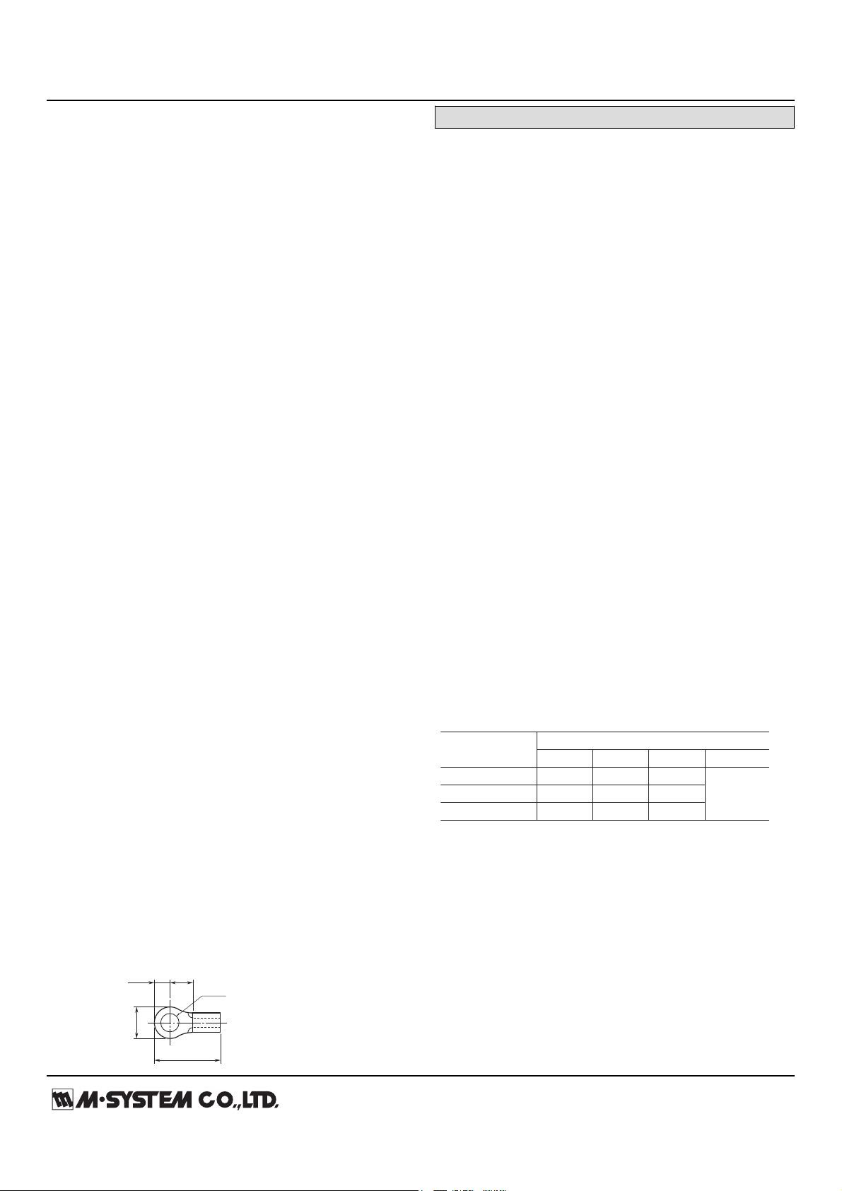
Recommended solderless terminal: Refer to the drawing on
the end of this section (unit: mm (inch)).
Applicable wire size: 0.3 to 0.75 mm
Screw terminal: Nickel-plated steel
Materials
Enclosure: Steel
Bezel: Flame-resistant resin (black)
2
Page 2
MODEL: 73VR21
http://www.m-system.co.jp/ 73VR21 SPECIFICATIONS ES-7395 Rev.11 Page 2/15
Front filter: Transparent resin
12max
6max
3max
4min
φ3.2
LINE NOISE
A/D CONVERSION (sec)
FILTER FREQ.
MEDIUM
*1 SLOW FAST
100 ms RAT
E
50 Hz 0.39 0.54 0.27
50/60 Hz*1 0.37 0.50 0.25 0.095
60 Hz 0.34 0.46 0.23
Multiplied by two (2) for RTD and potentiometer input.
*1. Standard setting
■ ANALOG INPUT UPDATE CYCLE
Isolation: Input 1 to input 2 to input 3 to input 4 to input 5 to
input 6 to input 7 to input 8 to input 9 to input 10 to input
11 to input 12 to trigger input to alarm output to power
input to FG to Ethernet
Burnout for T/C and RTD input: Upscale, Downscale or No
burnout selectable
Select ‘No Burnout’ to minimize the measuring errors
caused by the sensor/wire resistance and the burnout
sensing current.
With RTD input, the signal may go transiently to the
opposite direction from the burnout setting.
With DC input, the burnout setting is ignored and the
burnout sensing current is cancelled.
Cold junction compensation (CJC) for T/C input: CJC can be
enabled or disabled per each channel.
CJC sensor attached to Input 1 and Input 7* terminals.(Input
7 for the 73VR2108, 73VR2110 and 73VR2112)
Operating mode setting: Application software; burnout type,
cold junction compensation, line noise frequency, A/D
conversion mode setting available
Line noise filter: NMNR ratio to the line frequency and its
harmonic contents can be optimized. Factory set to 50/60
Hz mode for use with both frequencies.
Select either frequency for the most effective result.
A/D conversion mode: Fast, Medium or Slow selectable.
With Slow setting, data fluctuations are minimized with
limited sampling time (speed).
With Fast setting, sampling time (speed) can be high
through data fluctuations increase.
■ INTERFACE
Ethernet: 10BASE-T / 100BASE-TX automatically switched;
Conforms to IEEE 802 (10BASE-T) or IEEE 802.3 (100BASETX)
IP address: 192.168.0.1 (factory default setting)
Subnet mask: 255.255.255.0 (factory default setting)
Default gateway: None (factory default setting)
CF Card slot: Type I; for use with the cards’ operating
voltage 3.3 V
USB: Conforms to Version 1.1
■ DISPLAY
Display device: 5.5-inch TFT LCD
Display colors: 256
Resolution: 320 × 240 pixels
Pixel pitch: 0.12 × 0.35 mm
Note: The backlight can be replaced in M-System factory.
The LCD must be replaced at the same time.
INPUT SPECIFICATIONS
• DC Voltage
Input resistance: 900 kΩ min.
Excluding the case in which, with range setting other than
±12 V, ±6 V or ±3 V, a voltage exceeding ±1.3 V is applied.
Input range: ±60 mV, ±125 mV, ±250 mV, ±500 mV,
±1000 mV, ±3 V, ±6 V, ±12 V
■ THERMOCOUPLE
Input resistance: 900 kΩ minimum
Input type: (PR), K (CA), E (CRC), F (IC), T (CC), B (RH), R, S,
C (WRe 5-26), N, U, L, P (Platinel II)
Burnout sensing
Upscale: ≤ 130 nA
Downscale: ≤ 220 nA
No burnout: ≤ 10 nA
Burnout sensing time
K, E, J, N, L, P (upscale): ≤ 20 seconds
Others: ≤ 10 seconds
■ RTD (3-wire)
Excitation: 1.25 V / (1.25 kΩ + load resistance across the
terminals A – C); 1.00 mA with 10 Ω across A
– C; 0.55 mA with 1000 Ω across A – C
Allowable leadwire resistance: 20 Ω per wire
Input type: Pt 100 (JIS ’89), Pt 100 (JIS ’97, IEC), Pt 200, Pt
300, Pt 400, Pt 500, Pt 1000, Pt 50Ω (JIS ’81), JPt 100 (JIS
’89), Ni 100, Ni 120, Ni 508.4Ω, Ni-Fe 604, Cu 10 @ 25°C
Burnout sensing
Upscale or Downscale: ≤ 130 nA
No burnout: ≤ 10 nA
Burnout sensing time: ≤ 10 seconds
■ TRIGGER INPUT: Dry contact; detected ON at ≤ 0.8 V
Voltage across the terminals: ≤ 2.5 V
Current across the terminals: ≤ 4.0 mA
Page 3

MODEL: 73VR21
http://www.m-system.co.jp/ 73VR21 SPECIFICATIONS ES-7395 Rev.11 Page 3/15
OUTPUT SPECIFICATIONS
■ ALARM OUTPUT: Photo MOSFET relay (no polarity);
≤ 50 Ω at ON, ≥ 1 MΩ at OFF; OFF when not powered
Peak load voltage: 50 V max.
Continuous load current: 50 mA max.
Peak load current: 300 mA max. (≤0.1 sec.)
INSTALLATION
Power Consumption
•AC Power input:
Approx. 25 VA at 100 V
Approx. 35 VA at 240 V
•DC Power input: Approx. 11 W or 460 mA
Operating temperature: 0 to 50°C (32 to 122°F)
Display quality (e.g. decreased contrast) may deteriorate
when the recorder is used for a long time in an environment
exceeding 50°C. However, it is only a temporary
phenomenon. When the recorder is back in normal
temperature, full legibility is recovered. No damage in
performance.
Operating humidity: 30 to 85 %RH (non-condensing)
Allowable dust particles: 0.1 mg/m2 (no conductive particles)
Corrosive gas: Not allowed
Mounting: Panel flush mounting
Panel cutout dimensions: 137 × 137 mm (5.39”× 5.39”)
Weight
73VR2102, 73VR2104, 73VR2106: 2.3 kg (5.1 lbs)
73VR2108, 73VR2110, 73VR2112: 2.4 kg (5.3 lbs)
Caution: Use of UPS (switching time: without delay, output:
sine waveforms) is recommended to prevent data loss or CF
card damage by a loss of power during recording.
PERFORMANCE
Accuracy: See Tables 1 through 3.
Cold junction compensation error: (°C)
≤ ±[1.0 + |Ambient Temp. – 25| × 0.04]
(in stable ambient temperature; e.g. ±1.4°C at 15°C and
35°C)
Applicable with balanced terminal temperature.
Error will increase by imbalances caused by direct mounting
of the REM3 to the terminals.
Temp. coefficient: See Table 4.
Response time
DC of ±1000 mV or narrower ranges or T/C:
≤ [Sampling Time + 0.3 sec.] (0 – 90 %)
DC of ± 3 V or wider ranges:
≤ [Sampling Time + 0.5 sec.] (0 – 90 %)
RTD: ≤ [Sampling Time + 0.3 sec.] (0 – 90 %)
Calendar clock accuracy: Monthly deviation 3 minutes at
25°C
Insulation resistance: ≥ 100 MΩ with 500 V DC
(input 1 to input 2 to input 3 to input 4 to input 5 to input 6
to input 7 to input 8 to input 9 to input 10 to input 11 to
input 12 to trigger input to alarm output to power input to
FG to Ethernet)
Dielectric strength: 500 Vpeak @ 1 minute
(input 1 to input 2 to input 3 to input 4 to
input 5 to input 6 to input 7 to input 8 to
input 9 to input 10 to input 11 to input 12 to trigger input to
alarm output to power input or FG)
Peak value including both AC and DC (e.g. 354 V AC with 0
V DC).
Nominal withstand voltage between I/O (analog input,
trigger input and alarm output) and power input is
described 500 V peak. However, as far as FG terminal is
appropriately grounded, no dielectric breakdown will occur
between I/O (with or without grounding) and other terminals
when 2000 V AC is applied between FG and power input.
AC power input: 2000V AC @ 1 minute (power input to FG
or Ethernet) 500 V AC @ 1 minute (FG to Ethernet)
DC power input: 1250 V AC @ 1 minute (power input to FG
or Ethernet) 500 V AC @1 minute (FG to Ethernet)
Line noise normal mode rejection: ≥ 100 dB
Magnitude of the effects of normal mode 50/60 Hz noise,
with the most appropriate line noise filter frequency setting.
Each input circuit has a CR filter of sufficient large time
constant so that there will be little effect of line noise such
as 500 mV AC superposed on a thermocouple or ±60 mV
input.
Common mode noise rejection
Magnitude of the effects of voltages applied across the
terminal C and the ground terminal when there is no
potential difference among all the C terminals.
DC: N/A
AC, ±3 V, ±6 V, ±12 V: Approx. 86 dB
AC, other ranges: Approx. 120 dB
Common mode noise rejection between channels
Magnitude of the effects of DC/50/60 Hz voltages applied
across the terminals C of the present and the last scanned
channels.
DC, ±3 V, ±6 V, ±12 V: Approx. 100 dB
DC, other ranges: Approx. 120 dB
AC, ±3 V, ±6 V, ±12 V: Approx. 86 dB
AC, other ranges: Approx. 106 dB
STANDARDS & APPROVALS
CE conformity:
EMC Directive (2004/108/EC)
EMI EN 61000-6-4
EMS EN 61000-6-2
Low Voltage Directive (2006/95/EC)
EN 61010-1
Installation Category II
Page 4
MODEL: 73VR21
http://www.m-system.co.jp/ 73VR21 SPECIFICATIONS ES-7395 Rev.11 Page 4/15
Pollution Degree 2
*Accuracy: Applicable with the common mode voltage 0V
between C terminals of all channels and between C terminal of each channel and FG terminal.
The effects by the following factors are excluded: Fast
A/D conversion mode; temperature drift with the REM3
directly mounted to the I/O terminals; wire resistance;
burnout sensing current with upscale/downscale settings.
With 100 msec. storing rate, measured value may be susceptible to inaccuracies due to the fast update cycle. If this
is the case, please choose 500 msec. or slower rate.
Table 1. DC Voltage Input
INPUT RANGE ACCURACY (mV)
±60mV ±0.05
±125mV ±0.07
±250mV ±0.13
±500mV ±0.3
±1000mV ±0.5
±3V ±3
±6V ±5
±12V ±10
Table 2-1. Thermocouple Input, Celsius
T/C
USABLE CONFORMANCE
ACCURACY
RANGE (°C) RANGE (°C) (°C)
(PR) 0 to 1770 400 to 1770 ±4.6
K (CA) -270 to +1370 0 to 1370 ±1.5
E (CRC) -270 to +1000 0 to 1000 ±0.8
J (IC) -210 to +1200 0 to 1200 ±1.0
T (CC) -270 to +400 0 to 400 ±1.3
B (RH) 100 to 1820 700 to 1820 ±7.2
R -50 to +1760 400 to 1760 ±4.8
S -50 to +1760 400 to 1760 ±5.3
C (
WRe 5-26
) 0 to 2320 0 to 2320 ±4.9
N -270 to +1300 0 to 1300 ±1.9
U -200 to +600 0 to 600 ±1.3
L -200 to +900 0 to 900 ±1.0
P (
Platinel II
) 0 to 1395 0 to 1395 ±1.7
Remark 1) Measuring accuracy at 50µV emf.
Remark 2) CJC error is not included.
Table 2-2. Thermocouple Input, Fahrenheit
T/C
USABLE CONFORMANCE
ACCURACY
RANGE (°F) RANGE (°F) (°F)
(PR) 32 to 3218 752 to 3218 ±8.3
K (CA) -454 to +2498 32 to 2498 ±2.7
E (CRC) -454 to +1832 32 to 1832 ±1.5
J (IC) -346 to +2192 32 to 2192 ±1.8
T (CC) -454 to +752 32 to 752 ±2.4
B (RH) 212 to 3308 1292 to 3308 ±13.0
R -58 to +3200 752 to 3200 ±8.7
S -58 to +3200 752 to 3200 ±9.6
C (
WRe 5-26
) 32 to 4208 32 to 4208 ±8.9
N -454 to +2372 32 to 2372 ±3.5
U -328 to +1112 32 to 1112 ±2.4
L -328 to +1652 32 to 1652 ±1.8
P (
Platinel II
) 32 to 2543 32 to 2543 ±3.1
Table 3-1. RTD Input, Celsius
RTD USABLE RANGE (°C)
ACCURACY
at ≤ 0°C at ≥ 0°C
Pt 100 -200 to +850 ±0.4°C ±[0.4°C + Measured Val ue × 0.1%]
(JIS ’97, IEC) (±1.3°C at 850°C)
Pt 200 -200 to +850 ±0.3°C ±[0.3°C + Measured Val ue × 0.17%]
(±1.8°C at 850°C)
Pt 300 -200 to +850 ±[0.4°C + Measured Va lue × 0.08%] ±[0.4°C + Measured Val ue × 0.21%]
(±0.3°C at -200°C) (±2.2°C at 850°C)
Pt 400 -200 to +850 ±[0.4°C + Measured Va lue × 0.11%] ±[0.4°C + Measured Val ue × 0.21%]
(±0.2°C at -200°C) (±2.2°C at 850°C)
Pt 500 -200 to +850 ±[0.4°C + Measured Va lue × 0.13%] ±[0.4°C + Measured Val ue × 0.26%]
(±0.2°C at -200°C) (±2.6°C at 850°C)
Pt 1000 -200 to +850 ±[0.4°C + Measured Va lue × 0.15%] ±[0.4°C + Measured Val ue × 0.4%]
(±0.1°C at -200°C) (±3.8°C at 850°C)
Pt 100 -200 to +660 ±0.4°C ±[0.4°C + Measured Val ue × 0.1%]
(JIS ’89) (±1.1°C at 660°C)
JPt 100 -200 to +510 ±0.4°C ±[0.4°C + Measured Val ue × 0.1%]
(JIS ’89) (±1.0°C at 510°C)
Pt 50Ω (JIS ’81) -200 to +649
±0.5°C at ≤160°C, ±[0.4°C + Measured Val ue × 0.1%] at ≥160°C (±1.1°C at 649°C)
Ni 100 -80 to +260 ±0.3°C
Ni 120 -80 to +260 ±0.3°C
Ni 508.4Ω -50 to +280 ±[0.25°C + Measured Va lue × 0.06%] (±0.3°C at -50°C, ±0.5°C at 280°C)
Ni-Fe 604 -200 to +200 ±0.9°C at -200°C, ±0.6°C at -150°C, ±0.5°C at ±100°C, ±0.7°C at 200°C
Cu 10 @25°C -50 to +250 ±1.2°C
Remark 1) The lower the temperature range, the better the accuracy is for Pt 300, Pt 400, Pt 500, Pt 1000 and Ni 508.4Ω.
‘Measured Value’ in the equations is not an absolute value. Include the minus sign when calculating accuracies.
Max. operating voltage 300 V
Input 1 or 2 or 3 or 4 or 5 or 6 or 7 or 8 or 9 or 10 or 11 or
12 to power to FG or Ethernet: Reinforced insulation
Input 1 to 2 to 3 to 4 to 5 to 6 to 7 to 8 to 9 to 10 to 11 to 12
to trigger input to alarm output: Operational insulation
INPUT TYPE, RANGE, ACCURACY & TEMPERATURE COEFFICIENT
Page 5
MODEL: 73VR21
http://www.m-system.co.jp/ 73VR21 SPECIFICATIONS ES-7395 Rev.11 Page 5/15
Table 3-1. RTD Input, Fahrenheit
RTD USABLE RANGE (°F)
ACCURACY
at ≤ 32°F at ≥ 32°F
Pt 100 -328 to +1562 ±0.8°F ±[0.72°F + Measured Val ue × 0.1%]
(JIS ’97, IEC) (±2.4°F at 1562°F)
Pt 200 -328 to +1562 ±0.6°F ±[0.54°F + Measured Val ue × 0.17%]
(±3.3°F at 1562°F)
Pt 300 -328 to +1562 ±[0.72°F + Measured Value × 0.08%] ±[0.72°F + Measured Val ue × 0.21%]
(±0.5°F at -328°F) (±4.0°F at 1562°F)
Pt 400 -328 to +1562 ±[0.72°F + Measured Value × 0.11%] ±[0.72°F + Measured Val ue × 0.21%]
(±0.4°F at -328°F) (±4.0°F at 1562°F)
Pt 500 -328 to +1562 ±[0.72°F + Measured Value × 0.13%] ±[0.72°F + Measured Val ue × 0.26%]
(±0.3°F at -328°F) (±4.7°F at 1562°F)
Pt 1000 -328 to +1562 ±[0.72°F + Measured Value × 0.15%] ±[0.72°F + Measured Val ue × 0.4%]
(±0.2°F at -328°F) (±6.9°F at 1562°F)
Pt 100 -328 to +1220 ±0.8°F ±[0.72°F + Measured Val ue × 0.1%]
(JIS ’89) (±2.0°F at 1220°F)
JPt 100 -328 to +950 ±0.8°F ±[0.72°F + Measured Val ue × 0.1%]
(JIS ’89) (±1.7°F at 950°F)
Pt 50Ω (JIS ’81) -328 to +1200
±0.9°F at ≤320°F, ±[0.72°F + Measured Val ue × 0.1%] at ≥320°F (±1.9°F at 1200°F)
Ni 100 -112 to +500 ±0.6°F
Ni 120 -112 to +500 ±0.6°F
Ni 508.4Ω -58 to +536 ±[0.45°F + Measured Va lue × 0.06%] (±0.4°F at -58°F, ±0.8°F at 536°F)
Ni-Fe 604 -328 to +392 ±1.7°F at -328°F, ±1.1°F at -238°F, ±0.9°F at ±212°F, ±1.3°F at 392°F
Cu 10 @25°C -58 to +482 ±2.2°F
Remark 1) The lower the temperature range, the better the accuracy is for Pt 300, Pt 400, Pt 500, Pt 1000 and Ni 508.4Ω.
‘Measured Value’ in the equations is not an absolute value. Include the minus sign when calculating accuracies.
Table 4. Temperature Coef cient
INPUT TYPE TEMPERATURE COEFFICIENT
DC Voltage ±[Nominal Input Range × 0.015%]/°C or ±[Nominal Input Range × 0.008%]/°F
(e.g. ±0.018mV/°C with ±60mV range)
Thermocouple ±[Accuracy / 3] °C/°C or ±[Accuracy / 3] °F/°F (e.g. ±0.27°C/°C with E thermocouple)
RTD at ≤ 0°C or 32°F at ≥0°C or 32°F
Pt 100 ±0.041°C/°C ±[0.041°C + Measured Val ue × 0.026%]/°C
(JIS ’97, IEC) ±0.041°F/°F ±[0.041°F + Measured Val ue × 0.026%]/°F
Pt 200 ±0.044°C/°C ±[0.044°C + Measured Val ue × 0.033%]/°C
±0.044°F/°F ±[0.044°F + Measured Val ue × 0.033%]/°F
Pt 300 ±0.047°C/°C ±[0.047°C + Measured Val ue × 0.04%]/°C
±0.047°F/°F ±[0.047°F + Measured Val ue × 0.04%]/°F
Pt 400 ±0.05°C/°C ±[0.05°C + Measured Val ue × 0.052%]/°C
±0.05°F/°F ±[0.05°F + Measured Val ue × 0.052%]/°F
Pt 500 ±0.053°C/°C ±[0.053°C + Measured Val ue × 0.053%]/°C
±0.053°F/°F ±[0.053°F + Measured Val ue × 0.053%]/°F
Pt 1000 ±[0.068°C + Measured Val ue × 0.025%]/°C ±[0.068°C + Measured Val ue × 0.087%]/°C
±[0.068°F + Measured Val ue × 0.025%]/°F ±[0.068°F + Measured Val ue × 0.087%]/°F
Pt 100 ±0.041°C/°C ±[0.041°C + Measured Val ue × 0.024%]/°C
(JIS ’89) ±0.041°F/°F ±[0.041°F + Measured Val ue × 0.024%]/°F
JPt 100 ±0.041°C/°C ±[0.041°C + Measured Val ue × 0.023%]/°C
(JIS ’89) ±0.041°F/°F ±[0.041°F + Measured Val ue × 0.023%]/°F
Pt 50 ±0.039°C/°C ±[0.039°C + Measured Va lue × 0.021%]/°C
(JIS ’81) ±0.039°F/°F ±[0.039°F + Measured Val ue × 0.021%]/°F
Ni 100 ±0.028°C/°C ±[0.028°C + Measured Value × 0.01%]/°C
±0.028°F/°F ±[0.028°F + Measured Val ue × 0.01%]/°F
Ni 120 ±0.028°C/°C ±[0.028°C + Measured Value × 0.01%]/°C
±0.028°F/°F ±[0.028°F + Measured Val ue × 0.01%]/°F
Ni 508.4Ω ±0.046°C/°C ±[0.046°C + Measured Val ue × 0.018%]/°C
±0.046°F/°F ±[0.046°F + Measured Val ue × 0.018%]/°F
Ni-Fe 604
±0.058°C/°C at ≤-200°C, ±0.043°C/°C at -150°C, ±0.04°C/°C at -100°C, ±[0.047°C + Measured Val ue × 0.023%]/°C at ≥0°C
±0.058°F/°F at ≤-328°F, ±0.043°F/°F at -238°F, ±0.04°F/°F at -148°F, ±[0.047°F + Measured Value × 0.023%]/°F at ≥32°F
Cu 10 @25°C ±0.07°C/°C or ±0.07°F/°F
Page 6

MODEL: 73VR21
http://www.m-system.co.jp/ 73VR21 SPECIFICATIONS ES-7395 Rev.11 Page 6/15
APPLICATION SOFTWARE CD
• 73VR21x Builder Software: Model 73VR21BLD
OS Windows XP SP2, SP3 or Windows
Vista Business 32 bits or Windows
7 Professional 32 bits
Note: Proper software functions
may not be ensured under certain
conditions.
Screen area 1024 by 768 pixels
CD-ROM drive Windows supported CD-ROM drive
is used to install the software pro grams.
Card reader Used to read/write the CF Card
Mouse Windows supported
LAN card LAN card required to connect to
Ethernet;
10BASE-T or 100BASE-T cable
• 73VR Data Viewer: Model 73VRWV
OS Windows XP SP2, SP3 or Windows
Vista Business 32 bits or Windows
7 Professional 32 bits
Note: Proper software functions
may not be ensured under certain
conditions.
Screen area 1024 by 768 pixels or higher
Display color 65000 colors (16 bits)
Main memory (RAM)
512MB or higher recommended
2 GB recommended for Windows
Vista Business 32 bits or Windows
7 Professional 32 bits
CD-ROM drive Windows supported CD-ROM drive
is used to install the software pro grams.
Card reader Used to read/write the CF Card
Mouse Windows supported (Certain func-
tions of the 73VR may be compro mised if the mouse’s software
driver is not Windows standard.)
LAN card LAN card required to connect to
Ethernet;
10BASE-T or 100BASE-T cable
■ 73VRPAC2 (included in the product package)
• 73VR21x Builder Software: Model 73VR21BLD
Used to configure parameters on the PC.
- Parameter configurations can be downloaded to the recorder via Ethernet.
- Present setting on the 73VR21x can be uploaded and displayed on the PC.
- Configuration files can be converted into CSV.
• 73VR Data Viewer: Model 73VRWV
Used to show and analyze recorded data on the PC.
- Data stored in the CF Card can be called up on the PC screen via the CF Card Reader.
- Data stored in the CF Card can be sent by FTP and called up on the PC screen.
- Various analyzing functions
- Data, alarm history and comment files can be converted into CSV.
• PC Recorder Software: Model MSR128-V6
- The 73VR21x data can be sampled and stored in real time via Ethernet by the MSR128-V6.
• Instruction Manuals
- 73VR21x users manual
- 73VR21BLD users manual
- 73VRWV users manual
- MSR128-V6 users manual
PC REQUIREMENTS (provided by the user)
Page 7

MODEL: 73VR21
http://www.m-system.co.jp/ 73VR21 SPECIFICATIONS ES-7395 Rev.11 Page 7/15
• PC Recorder Software: Model MSR128-V6
NORMAL MODE (storing rates ≥500 ms) HIGH SPEED MODE (storing rates 100 / 200 ms)*
1
PC IBM PC/AT or compatible
OS Microsoft Windows XP SP1, SP2, SP3 or Windows Vista Business 32 bits or Windows 7 Professional
32 bits
Note: Proper software functions may not be ensured under certain conditions.
CPU Pentium III 800 MHz or higher Pentium IV 2.0 GHz or higher
1GHz higher for Windows Vista, Windows 7
Screen area 1024 by 768 pixels or better resolution
Display color 65000 colors (16 bits)
Video memory 2 MB minimum; 4 MB recommended 4 MB minimum
Main memory 256 MB recommended; 512 MB recommended;
1 GB recommended for Windows Vista, Windows 7 1 GB recommended for Windows Vista, Windows 7
Hard disk area Use an internal hard disk. *2 Use an internal hard disk. *2
Max. approx. 100 MB required per day. Max. approx. 500 MB required per day.
Printer Use a printer for Windows. The programs use Standard System Fonts used in Windows.
Use a printer driver for Standard System Fonts.
CD-ROM drive Used when installing the software program.
Card reader drive Used with devices which save data in a Compact Flash Card
Communication port RS-232C port (COM1 through COM5) supported LAN card by Windows
LAN card
*1. The 73VR1100 or the 73VR21x cannot be used in High Speed Mode.
*2. External (e.g. SCSI) devices may impair appropriate performance.
Page 8

MODEL: 73VR21
http://www.m-system.co.jp/ 73VR21 SPECIFICATIONS ES-7395 Rev.11 Page 8/15
EXTERNAL VIEW
■ FRONT VIEW
• 73VR21x
■ REAR VIEW
• 73VR2102, 73VR2104, 73VR2106
(2) Front Cover
(6) CF Card Access Indicator LED
(7) USB Connector
(3) CF Card Slot
(4) Eject Button
(5) Reset Button
(1) Touch Panel Screen
(13) Trigger Input Terminal
(14) Signal Input
Terminal Block
(14) Signal Input
Terminal Block
(14) Signal Input
Terminal Block
(8) Maintenance Jack
(10) LAN Port
(9) Power Indicator LED
(9) Power Indicator LED
(10) LAN Port
(11) Alarm Output Terminal
(12) Power Input Terminal
(13) Trigger Input Terminal
(11) Alarm Output Terminal
(12) Power Input Terminal
1A 1B 1C 3A 3B 3C 5A 5B 5C
2A 2B 2C 4A 4B 4C 6A 6B 6C
1A 1B 1C 3A 3B 3C 5A 5B 5C
2A 2B 2C 4A 4B 4C 6A 6B 6C
FG
ALM+ALM–U
(+)V(+)
TRG+TRG
–
7A 7B 7C 9A 9B 9C
11A11B11C
8A 8B 8C
10A10B10C12A12B12C
(8) Maintenance Jack
■ SIDE VIEW
• 73VR2108, 73VR2110, 73VR2112
• 73VR2108, 73VR2110, 73VR2112
FG
ALM+ALM–U
(+)V(+)
TRG+TRG
–
(1) Touch Panel Screen
Trend chart and other data views and setup views are
displayed.
(2) Front Cover
Access to the CF Card Slot.
(3) CF Card Slot
(4) Eject Button
Used to retrieve the CF Card.
(5) Reset Button
Used to restart the 73VR21x.
(6) CF Card Access Indicator LED
Red light turns on during the CF Card is accessed.
(7) USB Connector
Connect an USB ash-memory .
(8) Maintenance Jack
Unused
(9) Power Indicator LED
Light turns on while the power is supplied.
(
10
) LAN Port
Connects the LAN cable (10BASE-T or 100BASE-TX)
(11) Alarm Output Terminal
(12) Power Input Terminal
(13) Trigger Input Terminal
(14) Signal Input Terminal Block
Page 9

MODEL: 73VR21
http://www.m-system.co.jp/ 73VR21 SPECIFICATIONS ES-7395 Rev.11 Page 9/15
CONNECTION DIAGRAM
FG
JACK
USB
V(–)
U(+)
RJ-45 MODULAR JACK
CF CARD SLOT
INPUT 8
7A
7B
7C
INPUT 7
8A
8B
8C
Analog
Input
Circuit 7
Analog
Input
Circuit 8
INPUT 10
9A
9B
9C
INPUT 9
10A
10B
10C
Analog
Input
Circuit 9
Analog
Input
Circuit 10
INPUT 12
11A
11B
11C
INPUT 11
12A
12B
12C
Analog
Input
Circuit 11
Analog
Input
Circuit 12
TRIGGER
INPUT
ALM
+
ALM
–
ALARM
OUTPUT
TRG
+
TRG
–
Isolated
Alarm Output
Isolated
Trigger Input
Photo MOSFET Multiplexer
Floating A/D Converter
C
B
A
ext. wire
+
–
+
–
C
B
A
C
B
A
ext. wire
–
+
–
+
C
B
A
+
–
A
B
B
■DC INPUT ■T/C INPUT
• Upscale / No Burnout
■T/C INPUT
• Downscale Burnout
■RTD INPUT
Input Connection Examples
Remark 1:
Remark 2:
Remark 3:
Remark 4:
In order to prevent instability in measured values caused by noise entering through the I/O terminals,
grounding the signal shield to a most stable earth point in the environment is recommended.
The smaller is common mode voltage (DC and AC) between C terminals and between C and FG, the better is
measuring accuracy. Connecting between C terminals and if possible to FG will yield the best accuracy.
Resistor modules (model: REM3-250) can be connected to 1A through 12C terminals to convert current inputs
into voltage. However, it is not recommended when TC inputs are mixed because the heat developed on and
around the REM3 affects the cold junction compensation performance. We recommend that REM3 be connected
on a separate terminal board.
When the internal temperature sensors are used for CJC, temperature imbalance around the terminal block affects
greatly the CJC accuracy. In order to minimize such imbalance, do not use wires of large diameter which has large
heat dissipation. Be sure to close the terminal cover. Do not expose the module directly in the line of wind from a
cooling fan.
CJC
SENSOR
POWER
Ethernet
10BASE-T / 100BASE-TX
Micro
Computer
Control
Module
*1. Usable terminals depend upon the number of inputs.
metal leg
INPUT 2
1A
1B
1C
INPUT 1
2A
2B
2C
Analog
Input
Circuit 1
Analog
Input
Circuit 2
INPUT 4
3A
3B
3C
INPUT 3
4A
4B
4C
Analog
Input
Circuit 3
Analog
Input
Circuit 4
INPUT 6
5A
5B
5C
INPUT 5
6A
6B
6C
Analog
Input
Circuit 5
Analog
Input
Circuit 6
*1
CJC
SENSOR
metal leg
Page 10

MODEL: 73VR21
http://www.m-system.co.jp/ 73VR21 SPECIFICATIONS ES-7395 Rev.11 Page 10/15
DIMENSIONS unit: mm (inch)
144 (5.67)
172 (6.77)
29.5
(1.16)
2 to 26 panel thickness
(.08 to 1.02)
Attach the mounting bracket either on the top/bottom or on the sides.
151.5 (5.96)
144 (5.67)
136.5 (5.37)
151.5 (5.96)
136.5 (5.37)
■ 73VR2102, 73VR2104, 73VR2106
Page 11

MODEL: 73VR21
http://www.m-system.co.jp/ 73VR21 SPECIFICATIONS ES-7395 Rev.11 Page 11/15
Attach the mounting bracket either on the top/bottom or on the sides.
144 (5.67)
151.5 (5.96)
144 (5.67)
151.5 (5.96)
195 (7.68)
29.5
(1.16)
2 to 26 panel thickness
(.08 to 1.02)
136.5 (5.37)
136.5 (5.37)
■ 73VR2108, 73VR2110, 73VR2112
Page 12

MODEL: 73VR21
http://www.m-system.co.jp/ 73VR21 SPECIFICATIONS ES-7395 Rev.11 Page 12/15
PANEL CUTOUT (unit: mm)
137
+2
0
137
+2
0
137
+2
0
■ SINGLE MOUNTING ■ VERTICAL CLUSTERED MOUNTING (max. 3 units)
■ HORIZONTAL CLUSTERED MOUNTING
L
+2
0
137
+2
0
175 min
L
+2
0
L (mm)
Number
2
3
4
5
6
7
8
9
10
n
282
426
570
714
858
1002
1146
1290
1434
(114 × n) – 6
+2
0
175 min
Dimensional tolerance ±3% unless otherwise specified.
(±0.3 mm for <10 mm)
Usable panel thickness: 2 – 26 mm (0.08” – 1.02”)
SOFTWARE FUNCTIONS
■ NUMBER OF INPUT PEN POINTS
73VR2102: 2 points
73VR2104: 4 points
73VR2106: 6 points
73VR2108: 8 points
73VR2110: 10 points
73VR2112: 12 points
■ INPUT SIGNALS
Analog: DC mV and voltage, thermocouple and RTD
Discrete: Trigger input (1 point)
■ DATA STORING METHOD
Normal: Recording is manually initiated and stopped. Data
is continuously stored while the recording is on.
Auto: Recording is automatically initiated and stopped at a
predefined time.
Event recording: The recorder detects an external event by
trigger signal, and stores preset number of samples (max.
1200 respectively) before and after the moment of event.
Remote trigger: Data is automatically recorded while the
external trigger condition (input) is true.
■ STORING RATE
0.1 (DC voltage input only) 0.5, 1, 2, 5, 10 sec., 1, 10
minutes
■ DATA STORAGE
Data file: Stores momentary values in the storing rate and
their calculation result.
Alarm history file: Records time index information when
alarms are triggered and reset.
Oldest data is overwritten with new data when the number
of records reaches its limit.
Comment history file: Records comments written in trend
Page 13

MODEL: 73VR21
http://www.m-system.co.jp/ 73VR21 SPECIFICATIONS ES-7395 Rev.11 Page 13/15
views with time index. Oldest data is overwritten with new
data when the number of records reaches 1000 files.
Configuration file: Stores the 73VR21x setting.
File format: Binary
Oldest measured data is overwritten with new data or data
recording is stopped when the card memory is full.
■ ALARM
• Analog Alarm
Alarm setpoints: Max. 4 points per channel
Alarm type: High / Low
Deadband: Set in engineering unit values
Output: 1 point at Alarm Output TerminalStored
information: Date/time of alarm events (trip and reset), Pen
No., Tag Name and Alarm Message
Number of stored alarm events: Depends upon the CF Card
capacity.
128 MB 250 events
256 MB 500 events
512 MB or 1 GB 1000 events
■ CALCULATION FUNCTIONS
Number of channels: 12 channels
Operations
Arithmetic: Addition/subtraction, Multiplication, Division
Logical: AND, OR, NOT, XOR
Mathematical: Square root extractor, Power
Accumulation: Analog accumulation
Filter: Moving average, First order lag
Hold: Peak (maximum) hold (tracking increasing signal),
Peak (minimum) hold (tracking decreasing signal)
F value: F value
Alarm: Alarm trip can be programmed for calculated results.
■ DATA DISPLAY FUNCTIONS
• Trend View
Chart direction: Perpendicular or horizontal
Number of pens displayed: 2, 4, 6, 8 per view
Number of display views: 4
Chart speed: Chart speed is described as number of pixels
to plot single data sample. (pixel(s)/samples)
4, 1, 1/5, 1/32,
1/160 (not selectable with 100 msec. storing rate),
1/480 (not selectable with 100 msec. storing rate),
1/960 (not selectable with 100 msec. storing rate)
Display rate: 1 second
Pen thickness: Normal and wide
Digital indicator: Shows momentary value.
Alarm indicator: Shows alarm status of the channels
displayed on the screen.
Comment: Shows comments entered manually.
Scale: Linear and square root;
Switchable to the engineering unit scale.
• Bargraph View
Bargraph direction: Perpendicular or horizontal
Number of pens displayed: 2, 4, 6, 8 per view
Number of display views: 4
Display rate: 1 second
Digital indicator: Shows momentary value.
Alarm indicator: Shows alarm status of the channels
displayed on the screen.
Scale: Linear and square root;
Switchable to the engineering unit scale.
• Overview
Number of pens displayed: 2, 4, 6, 8, 16 per view
Number of display views: 13
Display rate: 1 second
Alarm indicator: Shows alarm status and date/time of the
last alarm trip and reset for the channels displayed on the
screen.
• Retrieve View: Shows data stored in the CF Card.
Number of pens displayed: 2, 4, 6, 8 per view
Number of display views: 4
Data search: Scrolling the chart, specifying a specific time
index, or searching by maximum/minimum values.
Long span view: Retrieved data is thinned out so that a
longer time span can be displayed on the chart.
• Alarm History View: Shows data stored in the alarm
history file.
Number of displayed alarm events: 16
Number of display views: 1
Display update: Automatically updated by a new event
Data search: Scrolling the view or specifying a specific time
index.
Jump: Scroll the view to an alarm event to show the relevant
data on Retrieve View.
• Comment History View: Shows data stored in the
comment history file.
Number of displayed alarm events: 16
Number of display views: 1
Data search: Scrolling the view or specifying a specific time
index.
Jump: Scroll the view to a comment to show the relevant
data on Retrieve View.
■ ETHERNET COMMUNICATION
• Dedicated Protocol
Real time communication: Transmits specific data to a host
PC installed with the PC Recorder Software (model:
MSR128).
FTP communication: Transmits data stored in the CF Card
using the FTP protocol to a host PC by the 73VR Data Viewer
(model: 73VRWV) installed in it. Data can be transmitted
Page 14

MODEL: 73VR21
http://www.m-system.co.jp/ 73VR21 SPECIFICATIONS ES-7395 Rev.11 Page 14/15
even during recording.
Supported Function Codes
CODE
NAME FUNCTION
01 Read Coil Status Reads DO
02 Read Input Status Reads DI
04 Read Input Register Reads Input Register
11 Fetch Communication Reads Status Word and
Event Counter Event Counter from
Comm. Event Counter
Exception Response
CODE
NAME FUNCTION
01 Illegal Function Function Not supported
02 Illegal Data Address Specifi ed address does
not exist
Supported Function Codes
ADDR. TYPE NAME
Coil (0X) 1 Discrete output
Input 1 Trigger input
Status
3 Discrete input (73VR2102)
(1X)
5 Discrete input (73VR2104)
7 Discrete input (73VR2106)
9 Discrete input (73VR2108)
11 Discrete input (73VR2110)
13 Discrete input (73VR2112)
14 – 25 Function data (discrete)
Input 1 – 24 F Measured data (analog)
Register (3X)
25 – 48 F Function data (analog)
Download, Upload: Software configurations created on the
73VR21x Configuration Builder (model:73VR21BLD) can be
downloaded to the 73VR21x. The configuration set up on
the 73VR21x can be uploaded and displayed on the
73VR21BLD.
• Modbus Protocol
Protocol: Modbus/TCP
Port No.: 502 (fixed)
IP address: Set on the recorder
Subnet mask: Set on the recorder
Default gateway: Set on the recorder
Max. number of 73VR21x connected simultaneously: 2
The CF Card is hot swappable: removable during data
recording. However, there may be a slight disturbance in
storing rate when the card is inserted.
• Screen Saver
The backlight is automatically turned off if the screen is
untouched for a certain time period.
• Bus Error Alert
An alarm is output at Alarm Output Terminal in case of
internal bus error.
• Writing/Reading Setting
The recorder’s present setting can be stored in a USB flashmemory. Setting stored in the memory can be read in to the
73VR21x.
• Hardware Setting
Burnout, Cold junction compensation, AD conversion mode,
line noise filter
• Field Calibration
■ OTHER FUNCTIONS
• Operation Lockout
With a password setting, unauthorized operations on the
Trend View, Bargraph View and Overview can be locked out.
• Data File Used Volume Information
A bargraph with % indication is provided on the screen to
show how much percent of the data file memory has been
used up.
0 – 49 % used: Green bargraph
50 – 79 % used: Amber bargraph
80 – 100 % used: Red bargraph
• Hot Swapping of the CF Card
Page 15

MODEL: 73VR21
http://www.m-system.co.jp/ 73VR21 SPECIFICATIONS ES-7395 Rev.11 Page 15/15
■ STORABLE TIME DURATION IN 128MB CF CARD
STORING
APPROXIMATE TIME DURATION
RATE
2 ch input 4 ch input 6 ch input 8 ch input 10 ch input 12 ch input
0.1 second 8 days 5 days 4 days 3 days 2 days 2 days
20 hours 18 hours 9 hours 10 hours 20 hours 10 hours
0.5 second 44 days 28 days 22 days 17 days 14 days 12 days
9 hours 22 hours 7 hours 17 hours 5 hours 4 hours
1 second 89 days 57 days 44 days 34 days 28 days 24 days
12 hours 20 hours 16 hours 3 hours 10 hours 9 hours
10 seconds 2 years 1 year 1 year 341 days 284 days 243 days
146 days 211 days 73 days 10 hours 12 hours 21 hours
1 minute --- 9 years 7 years 5 years 4 years 4 years
126 days 127 days 223 days 247 days 3 days
--- : Exceeds 10 years
Note 1) Data are calculated ones, and thus not guaranteed.
Note 2) Assuming 4 bytes per data per channel.
Note 3) A year is calculated as 365 days.
SYSTEM CONFIGURATION EXAMPLES
• Ethernet Connection
Ethernet
Ethernet
Card Reader
CF Card
■ INTERFACING WITH A PC
• Reading Data from CF Card
■ INDEPENDENTLY USED
Paperless Recorder
(models: 73VR21x)
Data Viewer
(model: 73VRWV)
PC Recorder Software
(model: MSR128)
Paperless Recorder
(models: 73VR21x)
Paperless Recorder
(models: 73VR21x)
Note: It is recommended to connect the 73VR21x to the PC using
straight cables via a switch/hub on the Ethernet.
Switch / Hub
Specifications are subject to change without notice.
 Loading...