

Page 1
INSTRUCTION MANUAL
MODBUS INTERFACE MODULE
(Modbus Wired Communication, Modbus-RTU Transparent 900 MHz Band Devices Use)
• Do not install the unit where it is subjected to continuous
BEFORE USE ....
Thank you for choosing M-System. Before use, please check
contents of the package you received as outlined below.
If you have any problems or questions with the product,
please contact M-System’s Sales Office or representatives.
■ PACKAGE INCLUDES:
Modbus interface module....................................................(1)
Antenna ...............................................................................(1)
Terminating resistor (110 Ω, 0.25 W) .................................(1)
■ MODEL NO.
Confirm Model No. marking on the product to be exactly
what you ordered.
■ INSTRUCTION MANUAL
This manual describes necessary points of caution when
you use this product, including installation, connection and
basic maintenance procedures.
This manual describes necessary points of caution when
you use this product, including installation, connection and
basic maintenance procedures.
For information on the introduction of wireless device, refer
to the 900 MHz band wireless device users manual (EM-
9085).
POINTS OF CAUTION
■ POWER INPUT RATING & OPERATIONAL RANGE
• Locate the power input rating marked on the product and
confirm its operational range as indicated below:
100 – 240V AC rating: 85 – 264V, 47 – 66 Hz,
approx. 15VA at 100V AC
approx. 20VA at 200V AC
approx. 21.5VA at 240V AC
24V DC rating: 24V ±10%, approx. 8.5W
vibration. Do not subject the unit to physical impact.
• Environmental temperature must be within -10 to +55°C
(14 to 131°F) with relative humidity within 30 to 90% RH
in order to ensure adequate life span and operation.
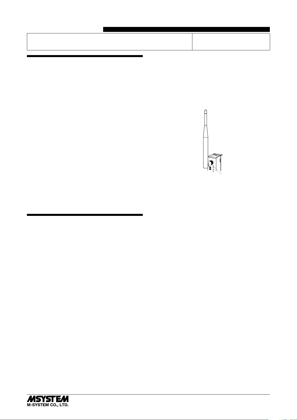
• Attachment and adjustment of sleeve antenna: Loosen
the connector (See the below figure), and rotate the antenna. Holding the antenna vertically, tighten the connector by hand. Make sure to fix the antenna firmly.
• Attachment of rooftop antenna: The magnet on the bottom
face allows the antenna to be attached on a metal box and
such. To obtain optimum performance from the antenna,
attach it on a metal plate (recommended dimension: 500
mm × 500 mm or more). However, in the case of connecting FE1 or FG of the power supply module to a metal
plate, the isolation between FE1 or FG and the internal
bus or internal power or antenna connector will be lost.
Tighten the connector with a specified torque (0.9 N∙m).
As a guide, finger-tighten the connector until it stops, and
then rotate it 10 to 15 degrees with a wrench. Do not force
the cable to bend beyond the acceptable bending radius
of 3 cm.
• Please note that using 7.5 m coaxial cable (model: CXSAC0SAD0Q0750) (OKI) for extension decreases transmission distance.
MODEL
R3-NMW1F
Connector
■ HOT-SWAPPABLE MODULES
• The module can be replaced while the power is ON. Be
sure to replace it when the module is not communicating with a host, as it may affect the system. Replacing
multiple modules at once may greatly change line voltage
levels. We highly recommend to replace them one by one.
■ ENVIRONMENT
• Indoor use.
• Attach the antenna to the unit.
• When heavy dust or metal particles are present in the
air, install the unit inside proper housing with sufficient
ventilation.
5-2-55, Minamitsumori, Nishinari-ku, Osaka 557-0063 JAPAN
Phone: +81(6)6659-8201 Fax: +81(6)6659-8510 E-mail: info@m-system.co.jp
■ WIRING
• Do not install cables close to noise sources (relay drive
cable, high frequency line, etc.).
• Do not bind these cables together with those in which
noises are present. Do not install them in the same duct.
■ AND ....
• The unit is designed to function as soon as power is supplied, however, a warm up for 10 minutes is required for
satisfying complete performance described in the data
sheet.
EM-8286 P. 1 / 10
Page 2
R3-NMW1F
CAUTION REGARDING RADIO FREQUENCY
■ FCC NOTICE
• This device complies with part 15 of the FCC Rules. Operation is subject to the following two conditions:
(1) This device may not cause harmful interference, and
(2) this device must accept any interference received, including interference that may cause undesired operation.
■ FCC CAUTION
• Changes or modifications not expressly approved by the
party responsible for compliance could void the user’s authority to operate the equipment.
■ NOTE
• This equipment has been tested and found to comply with
the limits for a Class A digital device, pursuant to part 15
of the FCC Rules. These limits are designed to provide
reasonable protection against harmful interference when
the equipment is operated in a commercial environment.
This equipment generates, uses, and can radiate radio
frequency energy and, if not installed and used in accordance with the instruction manual, may cause harmful
interference to radio communications. Operation of this
equipment in a residential area is likely to cause harmful
interference in which case the user will be required to correct the interference at his own expense.
• This transmitter must not be co-located or operated in
conjunction with any other antenna or transmitter.
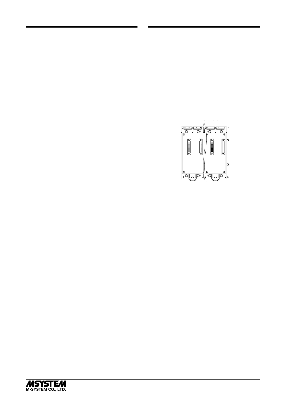
INSTALLATION
Use the Installation Base Model R3-BS, or Model R3-BSW
for free I/O address capability.
Before mounting the Network Interface Module onto the
Base, please do the following.
■ DATA ALLOCATION
Set the DIP switches (SW1, SW2) so as to assign the data
area size to each I/O module mounted on the base.
The data sent/received via Modbus is mapped according to
the setting.
See “COMPONENT IDENTIFICATION” and “MODBUS
I/O ASSIGNMENTS.”
■ MOUNTING TO THE BASE
I/O 1 I/O 2 I/O n
■ FCC RF EXPOSURE INFORMATION
• This equipment complies with FCC radiation exposure
limits set forth for an uncontrolled environment and
meets the FCC radio frequency (RF) Exposure Guidelines. This equipment should be installed and operated
keeping the radiator at least 20 cm or more away from
person’s body.
FCC ID: 2AOTF-0000008 (with no power supply)
FCC ID: 2AOTF-0000009 (24 V DC)
FCC ID: 2AOTF-0000010 (100 – 240 V AC)
Contains FCC ID: 2AKGW-1TD3016A1
With Model R3-BS base, mount the I/O Modules from the
left end (I/O 1) to the right in order that the Network Module assigns data areas from I/O 1.
Network Module(s) and Power Module are mounted basically at the right end though technically they could be
mounted in any position.
With Model R3-BSW base, there is no limitation in mounting positions as I/O address can be assigned freely to each
module using rotary switches equipped on the base.
5-2-55, Minamitsumori, Nishinari-ku, Osaka 557-0063 JAPAN
Phone: +81(6)6659-8201 Fax: +81(6)6659-8510 E-mail: info@m-system.co.jp
EM-8286 P. 2 / 10
Page 3
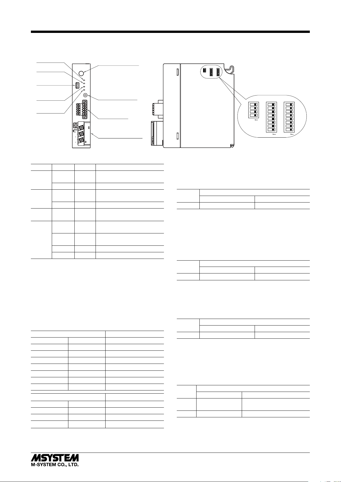
COMPONENT IDENTIFICATION
■ FRONT VIEW ■ SIDE VIEW
RUN LED
ERR LED
Maintenance
Connector
920Run LED
920Link LED
CFG2
NC
NC
NC
NC
Antenna Connector
RUN
ERR
920Run
920Link
CFG1
Configuration Jack
Tension clamp
Terminal
RUN Contact Output,
Power Input Terminal
R3-NMW1F
DIP SW
SW3
4
3
2
1
ON
SW2
8
7
6
5
4
3
2
1
ON
SW1
8
7
6
5
4
3
2
1
ON
■ STATUS INDICATOR LED
ID STAT U S COLOR FUNCTION
RUN*
1
ON Green
Output writable port: normal
communication
ON Red Wired: receiving data
ERR*
1
ON Green
Output writable port: communication error
ON Red Wired: transmitting data
920Run ON Green
920Link
ON Green
0.5 Hz
blinking
Green
Blinking Red
Wireless: normal communication
Wireless: coordinator is connected
Wireless: coordinator connection in process
Network authentication failure
ON Red NO detour
*1. Refer to “LED Function: SW3-4” below.
■ SIDE DIP SW
(*) Factory setting
• Data Allocation: SW1, SW2
2
Data Allocation Type*
must be assigned to each I/O module
slot position to specify how many data areas (four types) are
to be occupied by each module.
Two bits from SW1 and SW2 are assigned to each position,
so as to specify data areas for each of the slots No. 1 to 8.
Setting for No. 9 and later slots is identical to No. 8.
SW ASSIGNMENT SLOT
SW1-1 SW1-2 1
SW1-3 SW1-4 2
SW1-5 SW1-6 3
SW1-7 SW1-8 4
SW2-1 SW2-2 5
SW2-3 SW2-4 6
SW2-5 SW2-6 7
SW2-7 SW2-8 8
SW SETTING DATA ALLOCATION
OFF OFF 1
ON OFF 4
OFF ON 8
ON ON 16
*2. Refer to the specifications of the related series for the Data
Allocation Type of I/O modules.
• Dual Communication: SW3-1
When two network modules are mounted, one must be
‘Main’ (OFF) network and the other must be ‘Sub’ (ON) network. For single communication, the network module must
always be set to ‘Main’ (OFF).
SW
DUAL COMMUNICATION
MAIN (*)
SUB
SW3-1 OFF ON
• Input Error Data: SW3-2
Hold: When the communication from an input module is lost
due to the input module error, the network module holds the
signal and stands by until the communication recovers.
Set to ‘0’: When the communication from an input module
is lost due to the input module error, the network module
outputs ‘0.’
SW
INPUT ERROR DATA
HOLD (*)
SET ‘0’
SW3-2 OFF ON
• Main/Sub Switching Control: SW3-3
The host PC or PLC can choose whether ‘Main’ or ‘Sub’ bus
is used when the switching control is set to ‘Host.’
In ‘Normal’ mode, ‘Main’ bus is normally used, while ‘Sub’
bus is when the main communication has failed.
SW
MAIN/SUB SWITCHING CONTROL
NORMAL (*)
HOST
SW3-3 OFF ON
Note 1: Be sure to match this control mode for both network
modules in dual communication mode.
Note 2: Must be “OFF” in single communication mode.
• LED Function: SW3-4
Functions assigned to the front RUN and ERR LEDs can
be selected.
SW3-4
OFF (*)
RUN ERR
Green when normal
OFF when Timeout
LED FUNCTION
Green ON/blinking when abnormal
OFF when normal
ON Red when receiving Red when transmitting
5-2-55, Minamitsumori, Nishinari-ku, Osaka 557-0063 JAPAN
Phone: +81(6)6659-8201 Fax: +81(6)6659-8510 E-mail: info@m-system.co.jp
EM-8286 P. 3 / 10
Page 4

R3-NMW1F
CONFIGURATOR SOFTWARE SETTING
With configurator software, settings shown below are available.
Refer to the software manual of R3CON for detailed operation.
■ WIRED SETTING
ITEM SETTING RANGE DEFAULT
Communication timeout 2 – 32000 (100 msec.) 30 (100 msec.)
■ MODBUS SETTING
ITEM SETTING RANGE DEFAULT
Address 1 – 247 1
Data Mode RTU / ASCII RTU
Baud rate 38.4 kbps / 19.2 kbps / 9600 bps / 4800 bps 38.4 kbps
Parity Odd / Even / None None
Write enable port RS-485 / wireless RS-485
Slave or Relay Slave / Relay Slave
■ WIRELESS SETTING
ITEM SETTING RANGE DEFAULT
PAN-ID 0000 to FFFE (hexadecimal, 4 digits) 0000
Radio channel number 0 (invalid), 1 to 43 (selectable up to 10 channels) 0
Short address 0000 (invalid), 0001 to FFFD (hexadecimal, 4 digits) 0000
Network name English one-byte characters within 16 characters
(one-byte space, “-”, “_”, “.”, “@” are usable.)
Encryption key 0000...0 to FFFF...F (hexadecimal, 32 digits) 0000...0
Transmitter power output 0.16 mW / 1 mW / 20 mW 20 mW
Communication timeout 0 to 32767 (100 msec.) 30
Number of devices in a network 1 – 30 (devices) /
31 – 60 (devices) /
61 – 100 (devices) /
Fixed + Low speed movement
Packet filtering Disable / Enable Enable
Filter timeout on polling (100msec) 10 to 600 (100 msec.) 10
Fixed route Disable / Enable Disable
Destination short address 0000 to FFFD (hexadecimal, 4 digits) 0000
Temporary detour Disable / Enable Enable
Low speed moving mode Disable / Enable Disable
Set network quality Standard / Changing frequency • delaytime middle /
Changing frequency • delaytime large
Network join mode V3-compatible mode / Fast join mode V3-compatible mode
Retry times before route switching 1 to 3 (times) 3
Blank
1 – 30
Standard
5-2-55, Minamitsumori, Nishinari-ku, Osaka 557-0063 JAPAN
Phone: +81(6)6659-8201 Fax: +81(6)6659-8510 E-mail: info@m-system.co.jp
EM-8286 P. 4 / 10
Page 5

TERMINAL CONNECTIONS
• WITH SLEEVE ANTENNA
• WITH ROOFTOP ANTENNA
Connect the unit as in the diagram below.
■ EXTERNAL DIMENSIONS unit: mm (inch)
R3-NMW1F
280 (11.02)
130 (5.12)
4
5
6
27.5
(1.08)
[150 (5.91)
[R165(6.50)]
POSITIONING GUIDE
6 – M3
SCREW
1
2
3
6.2
(.24)
TERMINAL COVER
109 (4.29)45 (1.77)
[200 (7.87)]
Dia.3 (.12)
Dia.1.2 (.05)
80 (3.15)
36 (1.42)
Dia.27
(1.06)
[2500 (98.43)]
TERMINAL COVER
5-2-55, Minamitsumori, Nishinari-ku, Osaka 557-0063 JAPAN
Phone: +81(6)6659-8201 Fax: +81(6)6659-8510 E-mail: info@m-system.co.jp
19
(.75)
POSITIONING GUIDE
109 (4.29)
EM-8286 P. 5 / 10
Page 6
■ CONNECTION DIAGRAM
INTERNAL
INTERNAL
Caution: FE1 terminal is NOT a protective conductor termi-
nal.
R3-NMW1F
WIRING INSTRUCTIONS
■ TORQUE
Terminal wiring screw: 0.5 N·m
Maintenance
Connector
Configuration Jack
To Other
Modbus Devices
RUN CONTACT
OUTPUT
*
POWER INPUT
RUN +
RUN −
* Not provided with ‘No Power Supply’ type module.
ANTENNA CONNECTOR
USB CONNECTOR
JACK
FE
SLD
DG
DB
DA
1
4
U (+)
2
V (–)
3
*FE1
6
CONNECTOR
BUS
POWER
■ SOLDERLESS TERMINAL
Refer to the drawing below for recommended ring tongue
terminal size. Spade tongue type is also applicable. Solderless terminals with insulation sleeve do not fit.
Recommended manufacturer: Japan Solderless Terminal
MFG.Co.Ltd, Nichifu Co.,ltd
Applicable wire size: 0.75 to 1.25 mm
3max
4min
2
3.2 dia.
6max
12max
(mm)
■ TENSION CLAMP TERMINAL (Modbus)
2
Applicable Wire size: 0.2 to 1.5 mm
Stripped length: 10 mm
The following Phoenix Contact terminals are recommended:
AI 0.25-10YE 0.25 mm
AI 0.34-10TQ 0.34 mm
AI 0.5-10WH 0.5 mm
AI 0.75-10GY 0.75 mm
2
2
2
2
COMMUNICATION CABLE CONNECTIONS
■ SLAVE MODE
TERMINATOR
■ GATEWAY MODE
TERMINATOR
HOST PC
Tx+/Rx+
Tx–/Rx−
SG
Rx+
Rx–
R3-NMW1F
DA
DB
DG
SLD
FE
R3−NMW1F
DA
DB
DG
SLD
FE
FG
SLAVE DEVICE
DA
DB
DG
SLD
FG
FG
R3−NMW1F
DA
DB
DG
SLD
FE
FG
SLAVE DEVICE
DA
DB
DG
SLD
FG
FG
5-2-55, Minamitsumori, Nishinari-ku, Osaka 557-0063 JAPAN
Phone: +81(6)6659-8201 Fax: +81(6)6659-8510 E-mail: info@m-system.co.jp
EM-8286 P. 6 / 10
Page 7

MODBUS FUNCTION CODES & SUPPORTED CODES
■ Data and Control Functions
CODE NAME
01 Read Coil Status X Digital output from the slave (read/write)
02 Read Input Status X Status of digital inputs to the slave (read only)
03 Read Holding Registers X General purpose register within the slave (read/write)
04 Read Input Registers X Collected data from the field by the slave (read only)
05 Force Single Coil X Digital output from the slave (read/write)
06 Preset Single Register X General purpose register within the slave (read/write)
07 Read Exception Status
08 Diagnostics
09 Program 484
10 Poll 484
11 Fetch Comm. Event Counter
12 Fetch Comm. Event Log
13 Program Controller
14 Poll Controller
15 Force Multiple Coils X Digital output from the slave (read/write)
16 Preset Multiple Registers X General purpose register within the slave (read/write)
17 Report Slave ID X Slave type / ‘RUN’ status
18 Program 884/M84
19 Reset Comm. Link
20 Read General Reference
21 Write General Reference
22 Mask Write 4X Register
23 Read/Write 4X Register
24 Read FIFO Queue
R3-NMW1F
■ Exception Codes
CODE NAME
01 Illegal Function
02 Illegal Data Address
03 Illegal Data Value
04 Slave Device Failure
05 Acknowledge
06 Slave Device Busy
07 Negative Acknowledge
08 Memory Parity Error
X
Function code is not allowable for the slave
X
Address is not available within the slave
X
Data is not valid for the function
5-2-55, Minamitsumori, Nishinari-ku, Osaka 557-0063 JAPAN
Phone: +81(6)6659-8201 Fax: +81(6)6659-8510 E-mail: info@m-system.co.jp
EM-8286 P. 7 / 10
Page 8

R3-NMW1F
MODBUS I/O ASSIGNMENTS
ADDRESS DATA FORMAT NAME
Coil (0X) 1 – 1024 Digital Output (discrete output)
1025 Main / Sub Switching Command (valid only with SW3-3 set to ON)
Inputs (1X) 1 – 1024 Digital Input (discrete input)
1025 – 1040 Module Status
1041 – 1056 Error Status
1057 – 1072 Data Error Status
Input Registers (3X) 1 – 256 I Analog Input
257 – 768 F Analog Input
Holding Registers (4X) 1 – 256 I Analog Output
257 – 768 F Analog Output
I: Integer, 0 – 10000 (0 – 100%)
F: Floating (32-bit data cannot be accessed using floating addresses.)
Note: DO NOT access addresses other than mentioned above. Such access may cause problems such as inadequate operation.
• Module Status indicates whether individual I/O modules are mounted or not. The bit corresponding to the mounted slot
turns to “1,” and the unmounted slot to “0.”
• Error Status indicates error status for each module as described below. The bit corresponding to such module turns to “1.”
R3-TSx, R3-RSx, R3-US4: Input burnout
R3-DA16A: Power input in error or disconnected
R3-YSx: Output current error (e.g. load unconnected)
• Data Error Status indicates overrange (R3-US4: out of -10% to +110%; the other types: out of -15% to +115%) status for each
module. The bit corresponding to such module turns to “1.”
• Main / Sub Switching Commands given to the network modules result as follows:
‘MAIN’ MODULE ‘SUB’ MODULE OUTPUT MODE
1 0 Main bus is used; Red LED turns on at RUN LED of the I/O modules.
0 1 Sub bus is used; Green LED turns on at RUN LED of the I/O modules.
1 1 Main bus is used; Amber LED turns on at RUN LED of the I/O modules.
0 0 Output is invalid; RUN LED of the I/O modules turns off.
• Writing to Coil (0X) and Holding Registers (4X) is only available with either Wireless or Modbus communication. It is
available to change the configuration with Configurator Software (model: R3CON). Factory default setting is Modbus communication.
TRANSMISSION DATA ASSIGNMENTS
DIP SW located at the side of the module specifies each I/O module’s data allocation (occupied data area).
For example, when the data areas are assigned as shown below:
Module 1 4
Module 2 4
Module 3 4
Module 4 1
Module 5 1
Module 6 1
Module 7 1
Then the I/O data are assigned as in the table below:
ADDRESS POSITION ADDRESS POSITION
Input Registers (3X)
Holding Registers (4X)
1 – 4, 257 – 264 Slot 1 Coil (0X)
5 – 8, 265 – 272 Slot 2 65 – 128 Slot 2
9 – 12, 273 – 280 Slot 3 129 – 192 Slot 3
13, 281 – 282 Slot 4 193 – 208 Slot 4
14, 283 – 284 Slot 5 209 – 224 Slot 5
15, 285 – 286 Slot 6 225 – 240 Slot 6
16, 287 – 288 Slot 7 241 – 256 Slot 7
Inputs (1X)
1 – 64 Slot 1
For Coil (0X) and Inputs (1X), addresses 16 times assigned
data areas (Data Allocation Type) are allotted with the Data
Allocation Type ‘1’ and ‘4.’ With ‘8’ and ‘16,’ 64 (4 × 16) are
automatically allotted.
5-2-55, Minamitsumori, Nishinari-ku, Osaka 557-0063 JAPAN
Phone: +81(6)6659-8201 Fax: +81(6)6659-8510 E-mail: info@m-system.co.jp
EM-8286 P. 8 / 10
Page 9

MODULE STATUS, ERROR STATUS, DATA ERROR STATUS
Shows each module’s availability and error status.
R3-NMW1F
15
0
Module 1
Module 2
Module 3
:
Module 16
I/O DATA DESCRIPTIONS
The data allocations for typical I/O modules are shown below.
Refer to the manual for each module for detailed data allocations.
■ ANALOG DATA (16-bit data, models: R3-SV4, YV4, DS4, YS4 and US4, etc.)
16-bit binary data.
Basically, 0 to 100% of the selected I/O range is converted into 0 to 10000 (binary).
-15 to 0 % is a negative range represented in 2’s complement.
In case of R3-US4, -10 to 0% is a negative range represented in 2’s complement.
15
■ TEMPERATURE DATA (16-bit data, models: R3-RS4, TS4 and US4, etc.)
16-bit binary data.
With °C temperature unit, raw data is multiplied by 10. For example, 25.5°C is converted into 255.
With °F temperature unit, the integer section of raw data is directly converted into the data. For example, 135.4°F is converted into 135.
Minus temperature is converted into negative values, represented in 2’s complements.
0
15
0
■ ANALOG DATA (16-bit data, models: R3-CT4A, CT4B, etc.)
16-bit binary data.
Integer obtained by multiplying unit value (A) by 100.
In case of CLSE-R5, integer obtained by multiplying unit value (A) by 1000.
15
0
■ ACCUMULATED COUNT DATA (32-bit data, models: R3-PA2, PA4A, WT1, WT4, etc.)
32-bit binary data is used for accumulated counts and encoder positions.
Lower 16 bits are allocated from the lowest address to higher ones, higher 16 bits in turn.
32-bit data cannot be accessed using floating addresses.
15
+0
15
+1
0
Lower 16 bits
0
Higher 16 bits
5-2-55, Minamitsumori, Nishinari-ku, Osaka 557-0063 JAPAN
Phone: +81(6)6659-8201 Fax: +81(6)6659-8510 E-mail: info@m-system.co.jp
EM-8286 P. 9 / 10
Page 10

■ BCD DATA (32-bit data, models: R3-BA32A, BC32A, etc.)
1 : ON
32-bit binary data is used for BCD.
Lower 16 bits are allocated from the lowest address to higher ones, higher 16 bits in turn.
32-bit data cannot be accessed using floating addresses.
R3-NMW1F
15
+0
15
+1
0
Lower 16 bits
0
Higher 16 bits
■ 16-POINT, DISCRETE DATA (models: R3-DA16 and DC16, etc.)
15
0 : OFF
0
Input 1 (Output 1)
Input 2 (Output 2)
Input 3 (Output 3)
: :
Input 16 (Output 16)
■ DUAL COMMUNICATION MODE
RS485 or wireless port set for Write enable port can be dual-redundant.
■ MAIN / SUB SWITCHING CONTROL
R3 main network
(main/sub switching control)
Address : 01025 = 1
Address : 01025 = 0
Communication Status Start Main Lost Main Restored Switching by Host
R3 sub network
(main/sub switching control)
Address : 01025 = 1
Address : 01025 = 0
(1) (2) (3) (4) (5)
1) When the main/sub switching control for both main and sub network is set to ‘0’, all contact outputs are off, and analog
output modules output -15%.
2) When the main’s setting is switched to ‘1’, the output modules are in control of the main host device.
3) When a loss of communication is detected in the main network, the output signal is held for the preset time period. (Timer
is programmable with the PC Configurator Software, R3CON.) After the time has elapsed, the output control is switched
from the main to the sub network. Be sure to set an appropriate output signal to the sub network and switch the sub’s
setting to ‘1’ before such switching occurs.
4) The output modules’ control is not automatically switched back to the main’s when the main network is restored if the
main’s setting is ‘0’. Thus, if the main’s setting is ‘1’, the control is back to the main’s.
5) When both the main and the sub network modules are in communication, the output can be switched without delay.
5-2-55, Minamitsumori, Nishinari-ku, Osaka 557-0063 JAPAN
Phone: +81(6)6659-8201 Fax: +81(6)6659-8510 E-mail: info@m-system.co.jp
EM-8286 P. 10 / 10
 Loading...