

M.S.KENNEDY DAC2800S User Manual
5.4W
DC-DC
ISO-9001 CERTIFIED BY DSCC
DAC2800S
M.S.KENNEDY CORP.
CONVERTERS
4707 Dey Road Liverpool, N.Y. 13088 (315) 701-6751
FEATURES:
Wave Solderable Package
All Ceramic Capacitors
Surface Mount Magnetics
MIL STD 461C CR03 (DC-DC Converters)
80 Volt Input Transient Tolerent
Wide Supply Range - 11V to 50V
High Isolation - 500V
High Power Density - 15 W/in³
Output Voltage Adjustment - Standard
Remote Shutdown
Operates to 11V Input at 5W
Available with 12V or 15V Outputs
See DHC2800S Series for 3.3V and 5.0V Versions
Available Soon to DSCC SMD 5962-93093, 5962-94631,
5962-93094 and 5962-94630
Replaces Interpoint MSA2812S, MSA2815S and
IR ASA2812S, ASA2815S
MIL-PRF-38534 CERTIFIED
SERIES
DESCRIPTION:
The DAC2812S and DAC2815S DC-DC converters are higher output voltage companion devices to MSK's
DHC types. The DAC's provide the ruggedness, reliability and features required to meet the advanced design
challenges of today's hi-rel market. This has been accomplished while retaining a power density of 15 W/
in3 and 375 mW/gram of power/package performance. The use of advanced substrate and reflow soldering
techniques during construction results in a rugged, cost-effective and completely solderable package.
The DAC2800S hybrid converter series utilizes all ceramic capacitors, surface mount magnetics, and
ultrasonically bonded wires to provide reliable operation at all operating temperatures.
The DAC2800S series standard features include output fault monitoring and/or turn on voltage point
programming via the shutdown pin. All three functions may be implemented simultaneously with a minimum
of external components. An output voltage adjustment / load compensation pin which adjusts outputs
simultaneously is also standard.
Fault tolerant design protects these converters from most external circuit faults. The +output and output
adjust pins will withstand +25 V while the shutdown pin will withstand +50 V, protecting the converters
from a variety of system or board faults; e.g. solder bridges etc. Unique load fault protection circuitry allows
this converter to pull up loads having difficult static load line characteristics and allows short term load
excursions significantly beyond ratings in most applications.
A transformer isolated flyback converter topology operating at a switching frequency of 400 kHz allows
operation over a wide input voltage range. Internal filtering of outputs eliminates the need for external
capacitors in many applications.
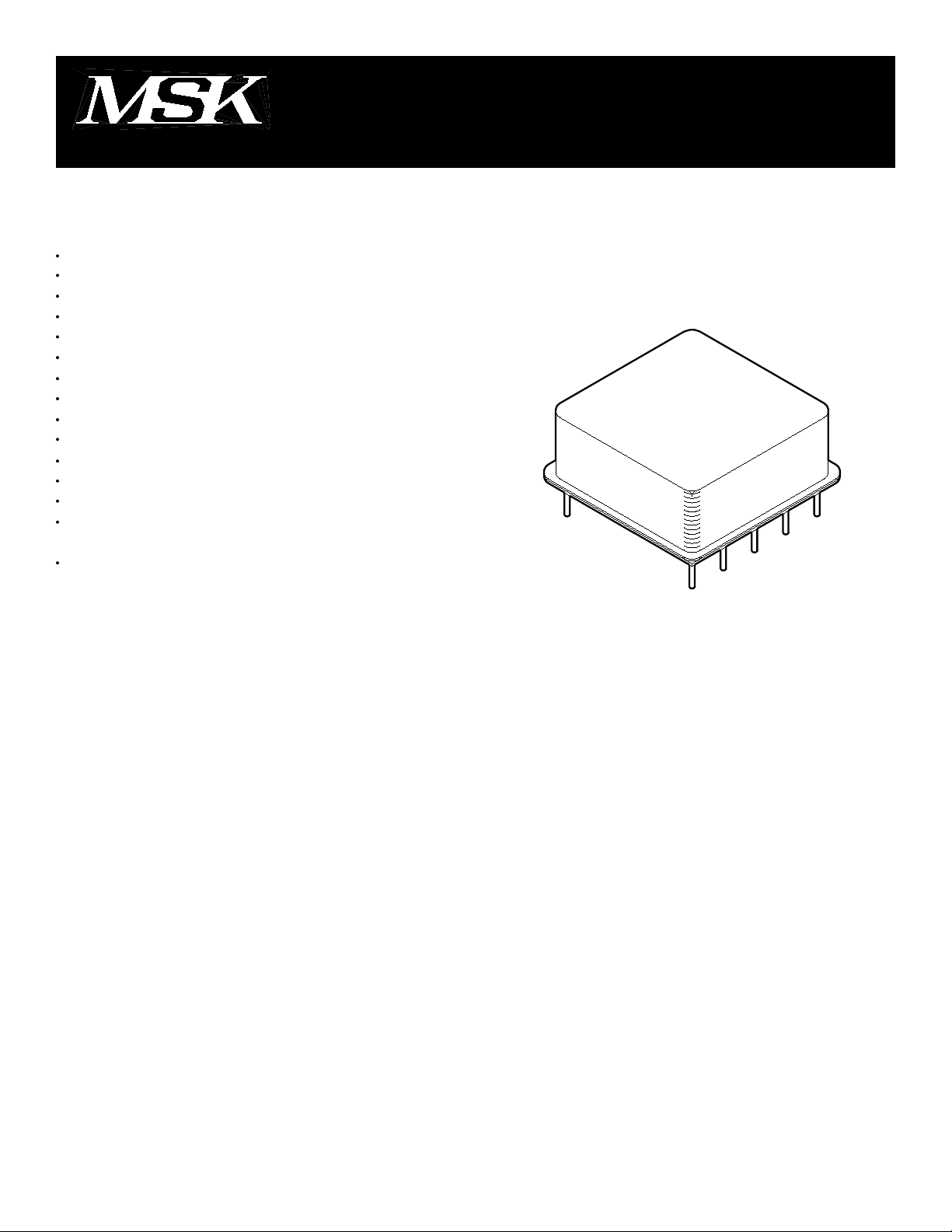
The 8-pin package is hermetically sealed and isolated from the internal circuits. Heat sinking is
recommended for full power operation at elevated ambient temperatures.
Rev. C 7/041
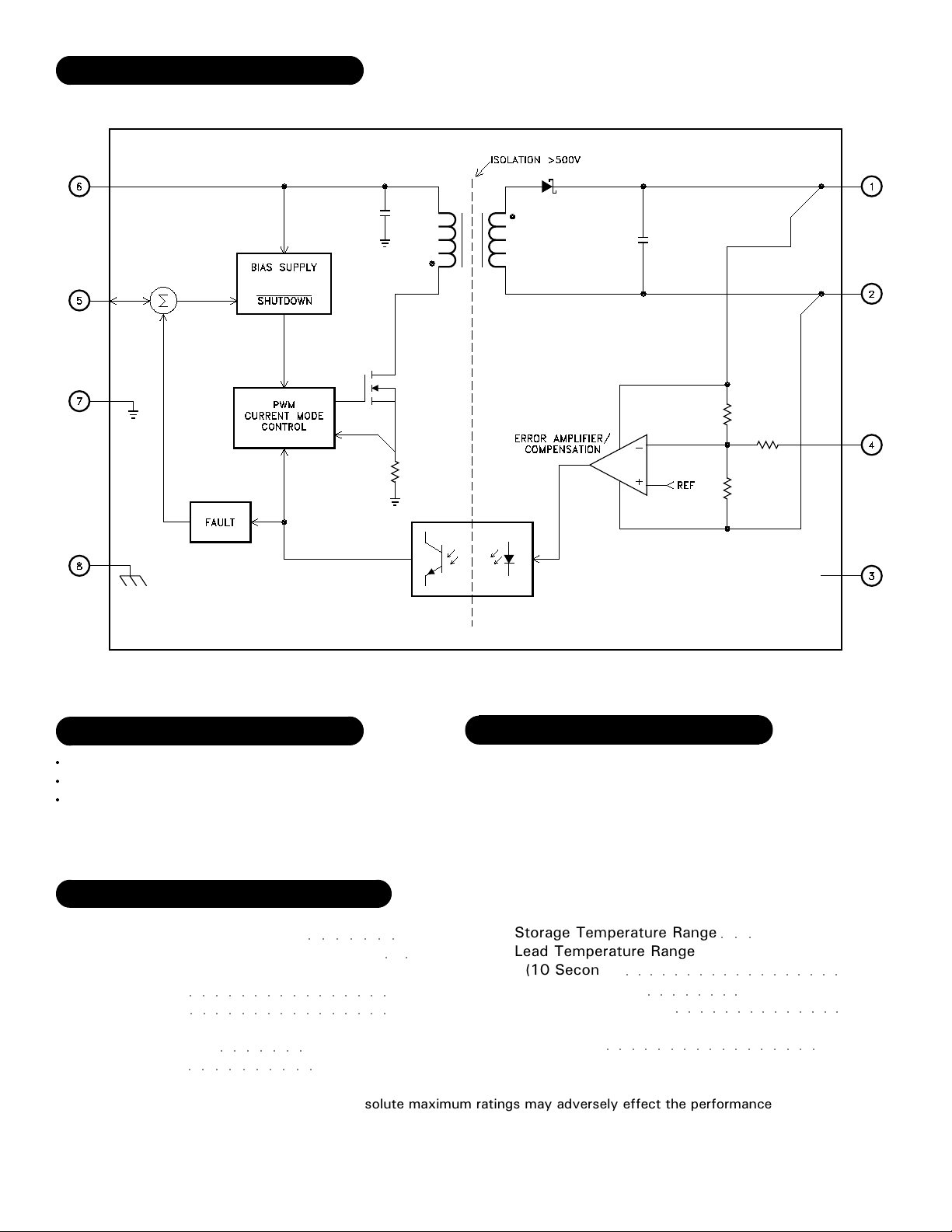
EQUIVALENT SCHEMATIC
TYPICAL APPLICATIONS
Isolated Step Down Power Supply
Microprocessor Power Source
Low Voltage Subsystem Power Source
PIN-OUT INFORMATION
+Output
1
-Output
2
NC
3
Adjust/Comp
4
Shutdown Plus
5
8
7
6
Case
-Input
+Input
ABSOLUTE MAXIMUM RATINGS
Storage Temperature Range
Input Voltage (pin 7 to pin 6)
VIN
Input Transient (pin 7 to pin 6 @ 50mS)
VINT
Output Current
IOUT
DAC2812S
DAC2815S
Case Temperature Range
TC
DAC2800S H/E
DAC2800S
○○○○○○○○○○○○○○○○
○○○○○○○○○○○○○○○○
○○○○○○○
○○○○○○○○○○
○○○○○○○
+50V
80V
○○
450mA
360mA
-55°C to +125°C
-40°C to +85°C
TST
Lead Temperature Range
TLD
(10 Seconds)
Power Dissipation
PD
Junction Temperature
TJ
Thermal Resistance
θJC
(Switches)
○○○○○○○○○○○○○○○○○○
○○○○○○○○
○○○○○○○○○○○○○○
○○○○○○○○○○○○○○○○○
NOTE: Continuous operation at or above the absolute maximum ratings may adversely effect the performance
and/or life of the device.
-65°C to +150°C
○○○
See Efficiency Curve
300°C
150°C
5.0°C/W
Rev. C 7/042
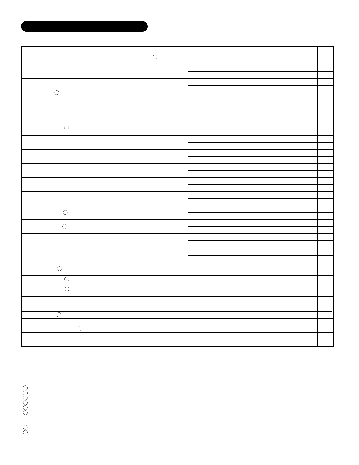
ELECTRICAL SPECIFICATIONS
DAC2812S
Parameter
Output Voltage
Output Current
Output Voltage Ripple
Input Current Ripple
Line Regulation
Load Regulation
Efficiency
Step Load Response
Step Load Recovery
Step Line Response
Step Line Recovery
Start Up Overshoot
Start Up Delay
Shutdown Delay
Shutdown Recovery
Input Voltage Range
Quiescent Current
Capacitive Load
Isolation
Short Circuit Current Limit
Switching Frequency
VOUT Adjustment Range
2
2
2
2
2
2
2
2
Min.
11.85
-
417
-
450
-
-
-
-
-
-
-
-
-
62
-
-
-
-
-
-
-
-
-
-
-
-
-
-
-
16
11
-
-
-
100
0.50
375
±10
DAC2812SDAC2812S H/E
Typ.
12.0
-
-
-
-
-
15
-
76
-
±5
-
±5
-
67
-
±350
-
80
-
±200
-
90
-
0
-
40
-
250
-
40
-
-
35
1.25
-
-
1.1
400
-
Max.
12.15
-
-
-
-
-
60
-
125
-
±30
-
±30
-
-
-
±500
-
200
-
±500
-
200
-
200
-
60
-
500
60
40
50
50
2.5
300
-
1.8
425
-
Units
VDC
VDC
mA
mA
mA
mA
mVrms
mVrms
mAp-p
mAp-p
mV
mV
mV
mV
%
%
mV
mV
µS
µS
mV
mV
µS
µS
mV
mV
mS
mS
µS
µS
mS
V
V
mA
mA
µF
MΩ
A
KHz
%
Test Conditions
IN≤50V
11V≤V
IN≤40V
16V≤V
BW=10KHz to 2MHz
BW=10KHz to 2MHz
LIN=2µH
IN=16, 28 and 40 VDC
V
OUT=0, 208 and 417mA
I
IN=16, 28 and 40 VDC
V
OUT=0, 208 and 417mA
I
OUT=208mA to/from 417mA
I
Transition TIme=30µS
OUT=208mA to/from 417mA
I
Transition TIme=30µS
IN=16V to/from 40V
V
Transition Time=30µS
IN=16V to/from 40V
V
Transition Time=30µS
OUT=5.4W MAX.
P
OUT=5W MAX.
P
Enabled, I
Disabled I
No Effect on DC Performance
Input to output or any pin to case @ 500V
7
POT=50KΩ
R
1
OUT=0mA
OUT=0mA
Group A
Subgroup
1
2,3
1
2,3
1
2,3
1
2,3
1
2,3
1
2,3
1
2,3
1
2,3
4
5,6
4
5,6
4
5,6
4
5,6
4
5,6
4
5,6
4
5,6
1,2,3
1,2,3
1,2,3
1,2,3
1,2,3
1
1
4
1
Min.
11.9
11.76
417
417
450
450
-
-
-
-
-
-
-
62
60
-
-
-
-
-
-
-
-
-
-
-
-
-
-
16
11
-
-
-
100
0.50
375
±10
Typ.
12.0
-
-
-
-
-
15
-
76
-
±5
-
±5
-
67
-
±350
-
80
-
±200
-
90
0
-
40
-
250
-
40
-
-
35
1.25
-
-
1.1
400
-
Max.
12.1
12.24
-
-
-
-
60
100
125
200
±25
±50
±25
±50
-
±500
±700
200
200
±500
±500
200
200
200
200
60
60
500
500
60
40
50
50
2.5
300
-
1.8
425
-
NOTES:
IN = 28V, IOUT = 417mA, TA=TC=25°C unless otherwise specified.
1
+V
Guaranteed by design but not tested. Typical parameters are representative of actual device performance but are for reference only.
2
Industrial grade and "E" suffix devices shall be tested to subgroups 1 and 4 unless otherwise specified.
3
Military grade devices ("H" suffix) shall be 100% tested to subgroups 1, 2, 3 and 4.
4
Subgroups 5 and 6 testing available upon request.
5
Subgroup 1, 4 TA=TC=+25°C
6
2, 5 TA=TC=+125°C
3, 6 TA=TC= -55°C
Device has internal shutdown feature that pulses the output with a low duty cycle during faults.
7
Consult DSCC SMD for electrical parameters for devices purchased as such.
8
3
Rev. C 7/04
 Loading...