

M.S.KENNEDY 5131 User Manual
查询MSK5131-1.7EZD供应商
MIL-PRF-38534 CERTIFIED
M.S.KENNEDY CORP.
HIGH CURRENT,
LOW DROPOUT
VOLTAGE REGULATORS
5131
SERIES
4707 Dey Road Liverpool, N.Y. 13088
(315) 701-6571
FEATURES:
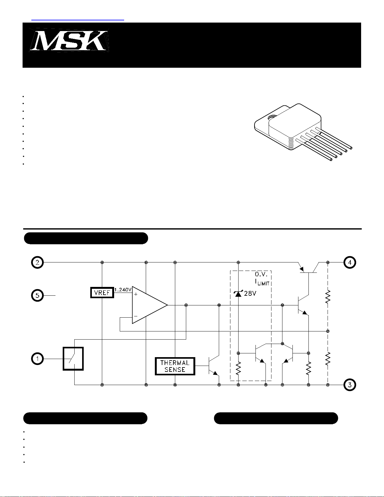
Electrically Isolated Top Tab or Z Tab SIP
Extremely Low Dropout Voltage: 350mV @ 3 Amps
Available in +1.5V,+1.7V,+1.8V,+1.9V,+2.5V,+3.3V,+5.0V and
+12.0V
TTL Level Enable Pin: Zero Current Shutdown Mode
Reverse Battery and Load Dump Protection
Low Ground Current: 42mA Typical at Full Load
1% Maximum Guaranteed Accuracy
Output Current to 3 Amps
Contact MSK for MIL-PRF-38534 Qualification Status
DESCRIPTION:
The MSK 5131 series voltage regulators are available in +1.5V,+1.7V,+1.8V,+1.9V,+2.5V,+3.3V,+5.0V and
+12.0V configurations. All boast ultra low dropout specifications due to the utilization of a super PNP output pass
transistor with monolithic technology. Dropout voltages of 350mV at 3 amps are typical in this configuration, which
drives efficiency up and power dissipation down. Accuracy is guaranteed with a 1% maximum output voltage
tolerance. The series also offers a TTL/CMOS compatible on/off enable function. The MSK 5131 series is packaged
in a space efficient 5 pin power SIP available in two styles with three lead bend options.
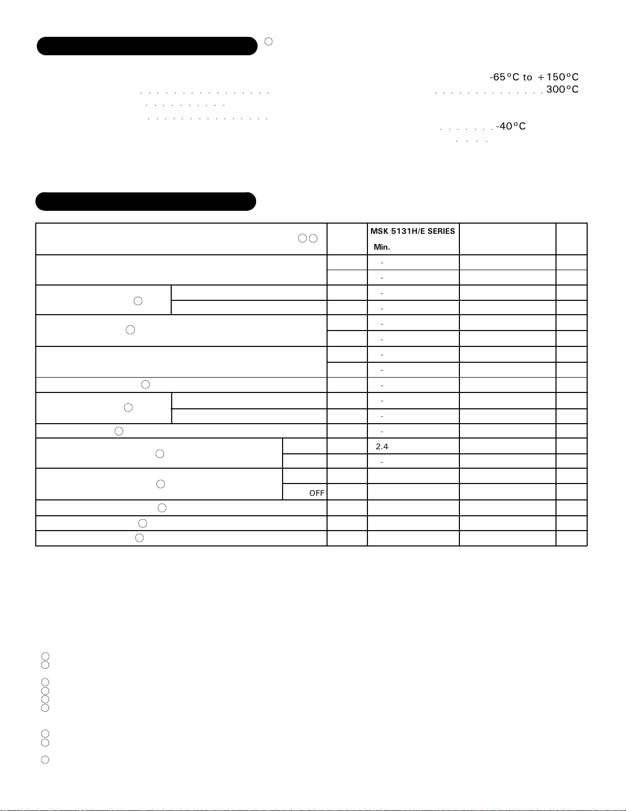
EQUIVALENT SCHEMATIC
TYPICAL APPLICATIONS
High Efficiency, High Current Linear Regulators
Constant Voltage/Current Regulators
System Power Supplies
Switching Power Supply Post Regulators
Battery Powered Equipment
PIN-OUT INFORMATION
1
Enable
2
Vin
3
Ground
4
Vout
5
N/C
1
Rev. B 2/06
ABSOLUTE MAXIMUM RATINGS
VINP
Input Voltage (100mS 1%D.C.)
VIN
Input Voltage
VEN
Enable Voltage
IOUT
Output Current
○○○○○○○○○○○○○○○○
○○○○○○○○○○
○○○○○○○○○○○○○○○
ELECTRICAL SPECIFICATIONS
9
-20V to +60V
26V
-0.3V to 26V
3.5A
Storage Temperature Range
TST
Lead Temperature
TLD
(10 Seconds Soldering)
Operating Temperature
TJ
MSK 5131 Series
MSK 5131H/E Series
-65°C to +150°C
○○○○○○○○○○○○○○
○○○○○○○
○○○○
-40°C to +85°C
-55°C to +125°C
300°C
Parameter
Output Voltage Tolerance
Dropout Voltage
Load Regulation
2
8
Line Regulation
Output Current Limit
Ground Current
Output Noise
2
2
2
Enable Input Voltage
Enable Input Current
Shutdown Output Current
Thermal Resistance
Thermal Shutdown
2
2
Test Conditions
1
3
Group A
Subgroup
IOUT=10mA; VIN=VOUT+1V
∆VOUT=-1%; IOUT=100mA
∆VOUT=-1%; IOUT=3A
VIN=VOUT+1.5V
10mA ≤ IOUT ≤ 2.5A
(VOUT +1V) ≤ VIN ≤ 26V
IOUT=10mA
VOUT=0V; VIN=VOUT+1V
VIN=VOUT+1V; IOUT=1.5A
VIN=VOUT+1V; IOUT=3A
CL=20µF; 10Hz ≤ f ≤ 100KHz
2
HIGH/ON
LOW/OFF
2
HIGH/ON
LOW/OFF
2
VENABLE ≤ 0.8V
Junction to Case @ 125°C
TJ
MSK 5131H/E SERIES
Min.
1
2,3
1
1
1
2,3
1
2,3
-
-
-
1
1
1
1
-
-
-
-
-
-
-
-
-
-
-
-
-
-
-
2.4
-
-
-
-
-
-
Typ.
±0.5
±1.0
80
350
±0.2
±0.3
±0.05
±0.5
4.5
20
42
400
1.2
1.2
20
-
10
2.1
135
Max.
±1.0
±2.0
175
600
±1.0
±2.0
±0.5
±1.0
5.0
45
-
-
-
0.8
600
2
500
2.4
-
MSK 5131 SERIES
2.4
Typ.
±0.5
-
-
-
-
-
-
-
-
-
-
-
-
-
80
350
±0.2
±0.3
±0.05
±0.5
4.5
20
42
400
1.2
1.2
20
-
-
-
-
-
-
10
2.1
135
Min.
Max.
±1.0
200
625
±1.2
-
±0.6
-
5.0
45
-
-
-
0.8
600
2
500
2.5
-
Units
%
%
mV
mV
%
%
%
%
A
mA
mA
µV
V
V
µA
µA
µA
°C/W
°C
NOTES:
Output decoupled to ground using 27µF minimum capacitance unless otherwise specified.
1
This parameter is guaranteed by design but need not be tested.
2
Typical parameters are representative of actual device performance but are for reference only.
All output parameters are tested using a low duty cycle pulse to maintain TJ = TC.
3
Industrial grade and "E" suffix devices shall be tested to subgroup 1 unless otherwise specified.
4
Military grade devices ('H' suffix) shall be 100% tested to subgroups 1,2 and 3.
5
Subgroup 1
6
Subgroup 2
Subgroup 3
Please consult the factory if alternate output voltages are required.
7
Due to current limit, maximum output current may not be available at all values of VIN-VOUT and
8
temperatures. See typical performance curves for clarification.
Continuous operation at or above absolute maximum ratings may adversely effect the device
9
performance and/or life cycle.
TC=+25°C
TJ=+125°C
TA=-55°C
2
Rev. B 2/06
 Loading...