

MSK MSK645, MSK645B Datasheet
M.S.KENNEDY CORP.
ISO-9001 CERTIFIED BY DSCC
HIGH PERFORMANCE,
HIGH VOLTAGE
VIDEO DISPLAY DRIVER
645
4707 Dey Road Liverpool, N.Y. 13088
FEATURES:
70 Vpp Output Voltage
150 MHz Typical Bandwidth
Transition Times Typically <3.0 nS
Cost and Space Efficient Package
Electrically Isolated Case
Gain Fixed Internally
MIL-PRF-38534 CERTIFIED
(315) 701-6751
DESCRIPTION:
The MSK 645 is an amplifier designed specifically to suit the needs of todays high resolution CRT display moni-
tors. With a typical bandwidth of 150 MHz and transition times typically under 3.0nS the MSK 645 can easily drive
monitors with resolutions of up to 1280 x 1024. The output can swing up to 70 Vpp and gain is internally set to
minimize external component count. The MSK 645(B) is available screened to MIL-PRF-38534 and comes in a space
efficient package that is electrically isolated from the internal circuitry and can be attached directly to a heat sink for
efficient thermal dissipation.
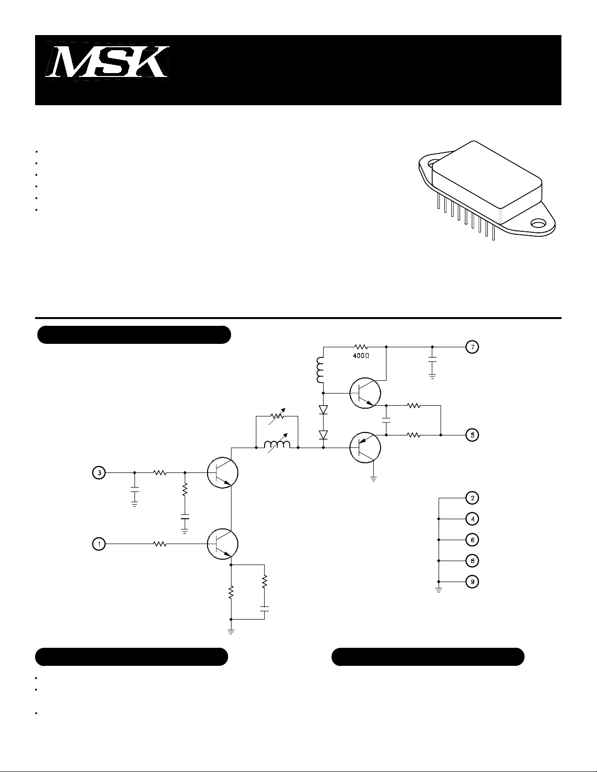
EQUIVALENT SCHEMATIC
TYPICAL APPLICATIONS
CRT Driver for SVGA
Display Driver for Systems with up to
1280 x 1024 Display Resolution
High Voltage Fixed Gain Amplifier
PIN-OUT INFORMATION
1
Video Input
2
Ground
3
VBIAS
4
Ground
5
Video Output
6
7
8
9
Ground
+VHV
Ground
Ground
Rev. B 12/011
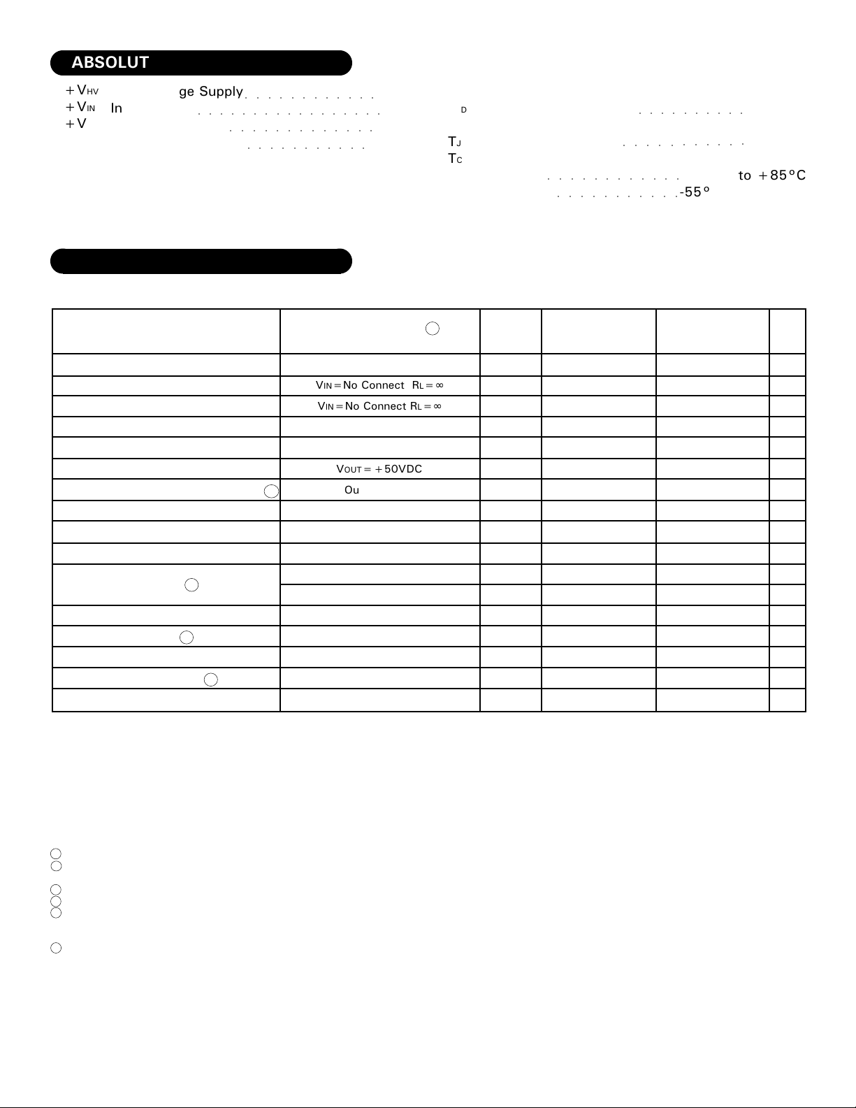
ABSOLUTE MAXIMUM RATINGS
+VHV
+VIN
+VBIAS
IOUT
High Voltage Supply
Input Voltage
Bias Input Voltage
○○○○○○○○○○○○○○○○○
○○○○○○○○○○○○○
Peak Output Current
○○○○○○○○○○○○
○○○○○○○○○○○
ELECTRICAL SPECIFICATIONS
Parameter
STATIC CHARACTERISTICS
Quiescent Current (VHV)
Quiescent Current (+VBIAS)
VHV Power Supply Range
VBIAS Power Supply Range
Video Input Voltage
Thermal Resistance (junction-to-case) 2
+90V
±5V
+10V
200mA
Test Conditions
VIN=No Connect RL=∞
VIN=No Connect RL=∞
VOUT=+50VDC
Output Stage
Storage Temperature Range
TST
Lead Temperature Range
TLD
○○○○○○○○○○
-65°C to +150°C
+300°C
(Solder 10 Seconds)
Junction Temperature
TJ
Case Operating Temperature
TC
MSK645
MSK645(B)
1
Group A
Subgroup
1,2,3
1,2,3
1,2,3
○○○○○○○○○○○○
○○○○○○○○○○○
MSK 645(B) MSK 645
Min. Typ. Max.
-
-
-
-
20
4
0.5
-
-
○○○○○○○○○○○
Min. Typ. Max.
2.0
0.6
0.5
0.01
90
60
10
5
1.2
0.85
25
0.4
27
+175°C
-40°C to +85°C
-55°C to +125°C
0.6
0.01
60
5
0.85
25
2.0
0.5
90
10
1.3
27
-
-
20
4
-
Units
mA
mA
V
V
V
°C/W
DYNAMIC CHARACTERISTICS
Video Output Voltage
6
Video Gain
Video Gain Flatness 2
Video Output Rise/Fall Time
Video Output Overshoot 2
Bandwidth -3dB
F=1MHz;VOUT=+15Vto+45V
F=10Hz to 60MHz;VOUT=30VPP
VOUT=10VPP VINTR=10nS
High Level
Low Level
VOUT=+15Vto+45V
CL=6.5pF
NOTES:
+VHV=60V; +VBIAS=5V; RL=10KΩ; unless otherwise specified.
1
Parameter is guaranteed by design but not tested. Typical specifications are representative of actual device
2
performance at 25°C but are for reference only.
Military grade devices ('B' suffix) shall be 100% tested to subgroups 1,2,3 and 4.
3
Subgroup 5 and 6 testing available upon request.
4
Subgroup 1,4 TA=TC=+25°C
5
Subgroup 2,5 TA=TC=+125°C
Subgroup 3,6 TA=TC=-55°C
Refer to the video clip point curve on the Typical Performance Curves page.
6
10
80
5.0
12
V
-
V
V/V
dB
nS
%
MHz
-
4
4
4
-
4
-
4
100
50
45
59
-
62
±1.0
-
3.0
-
-
150
-
50
59
10
5
80
±2.0
4.0
10
-
-
5
45
60
±1.0
3.0
-
150
±3.0
-
-
-
-
100
2
Rev. B 12/01
 Loading...