

MSK MSK643, MSK643B Datasheet
M.S.KENNEDY CORP.
ISO 9001 CERTIFIED BY DSCC
WIDE BANDWIDTH,
VERY HIGH VOLTAGE
CRT VIDEO AMPLIFIER
643
4707 Dey Road Liverpool, N.Y. 13088
FEATURES:
Negative Output Voltage for Grid Drive
2.5nS Transition Times
Drives 8.5pF Capacitive Load With Ease
DC Coupled for Output Level Adjust
175MHz Bandwidth
75Vpp Output Swing
Replacement for CR3424R
MIL-PRF-38534 CERTIFIED
(315) 701-6751
DESCRIPTION:
The MSK 643(B) is a wide bandwidth, high voltage color or monochrome CRT video amplifier designed specifically
to drive the grid of today's most demanding high resolution CRT monitors. The MSK 643(B) is a transimpedance
amplifier capable of achieving a ±40V output voltage swing with an input current of ±10mA. The output of the
amplifier is DC biased at half the power supply voltage. Transition times in the range of 2.5nS enable the MSK 643
to drive 10nS pixels with ease and make it ideally suited for monitors with 1280 x 1024 or higher display resolutions.
The MSK 643 is mounted in a space efficient 9 pin single in-line bathtub package with two mounting tabs for direct
mounting to a heat sink or chassis.
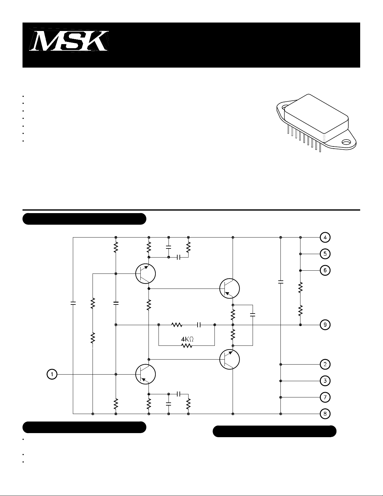
EQUIVALENT SCHEMATIC
TYPICAL APPLICATIONS
CRT Driver for Color and
Monochrome Monitors
High Voltage Transimpedance Amplifier
Ultra High Speed Amplifier for
Test Equipment
PIN-OUT INFORMATION
1
Inverting Input
2
Ground
3
Ground
4
-Vee
5
-Vee
1
6
-Vee
7
Ground
8
Ground
9
Output
Rev. B 12/01
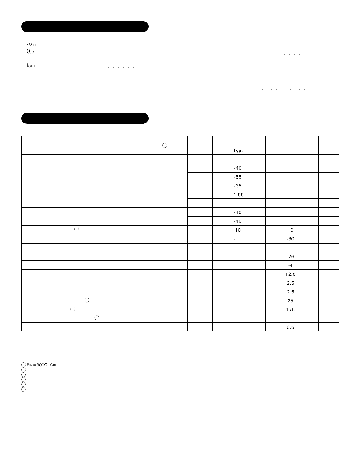
ABSOLUTE MAXIMUM RATINGS
-VEE
θJC
Supply Voltage
○○○○○○○○○○○○○○
Thermal Resistance
○○○○○○○○○○○
(Junction to Case)
IOUT
Peak Output Current
ELECTRICAL SPECIFICATIONS
Parameter
STATIC
Power Supply Current
Input Bias Voltage
Output Offset Voltage
Input Capacitance
Power Supply Range
DYNAMIC CHARACTERISTICS
Output Voltage High
Output Voltage Low
Voltage Gain
Rise Time
Fall Time
Overshoot (Adjustable)
-3dB Bandwidth
Low Frequency Tilt Voltage
Linearity Error
2
2
2
2
-100V
27°C/W
○○○○○○○○○○
Test Conditions
VIN=N/C
VIN=N/C
VIN=N/C
VIN=0.7V
Derated Performance
f=10KHz
f=10KHz
VIN=2VPP; f=10KHz
VOUT=40VPP
VOUT=40VPP
VOUT=20VPP
VOUT=20VPP
f=1KHz
f=10KHz; 5VPP≤VOUT≤50Vpp
250mA
1
TST
Storage Temperature Range
TLD
Lead Temperature Range
(10 Seconds)
TC
Case Operating Temperature
MSK643
MSK643B
TJ
Junction Temperature
○○○○○○○○○○○○
○○○○○○○○○○○
-Vee=-80V Unless Otherwise Specified
Min.
-
-
-
-1.4
-1.35
-38
-36
-
-60
-74
-
10.5
-
-
-
125
-
-
MSK 643B
Typ.
-40
-55
-35
-1.55
-
-40
-40
10
-80
-76
-4
12.5
2.5
2.5
25
175
-
0.5
Group A
Subgroup
1
2
3
1
2,3
1
2,3
-
-
4
4
4
4
4
-
-
-
4
-65°C to +150°C
○○○○○○○○○○
-55°C to +125°C
○○○○○○○○○○○○
MSK 643
Max.
-45
-65
-45
-1.7
-1.8
-42
-44
-100
14.5
3.4
3.4
1.5
Min.
-
-
-
-1.55
-1.3
-
-37
-
-
-
-60
-
-74
-6
-
10
-
-
-
-
-
120
-
5
-
300°C
-40°C to +85°C
175°C
-50
-43
-6
15
3.5
3.5
1.5
5
Units
mA
mA
-
mA
-
V
-
V
V
-
-
V
pF
V
-
V
V
V/V
nS
nS
%
-
MHz
-
V
%
Typ.
-40
-55
-35
-
-40
-
10
-80
-76
-4
12.5
2.5
2.5
25
175
-
0.5
Max.
-1.8
-100
NOTES:
1
RIN=300Ω, CIN=100pF, CLOAD=8.5pF, RL=∞, unless otherwise specified (See Figure 1).
2
Guaranteed by design but not tested. Typical parameters are representative of actual device performance but are for reference only.
3
Industrial grade devices shall be tested to subgroups 1 and 4 unless otherwise specified.
4
Military grade devices ('B' suffix) shall be 100% tested to subgroups 1,2,3 and 4.
5
Subgroup 5 and 6 testing available upon request.
6
Subgroup 1,4 TA=TC=+25°C
Subgroup 2,5 TA=TC=+125°C
Subgroup 3,6 TA=TC=-55°C
Rev. B 12/012
 Loading...