

MSK MSK621, MSK621B Datasheet
4707 Dey Road Liverpool, N.Y. 13088
M.S.KENNEDY CORP.
(315) 701-6751
FEATURES:
230 MHz Video Bandwidth With Vout=4Vpp
Transition Times Less Than 2.0nS With Vout=4Vpp
0 To 4 Volt High Input Impedance DC Drive Control With ±3dB Range
0 To 4 Volt High Input Impedance DC Contrast Control With 40dB Range
Externally Gated Comparator for Brightness Control
Simple To Parallel For RGB Color Tracking
0.0V to 9.0V Output Voltage Swing Capability
On Board Accurate Reference Voltage Generator
Available Fully Qualified to MIL-PRF-38534
WIDE BANDWIDTH VIDEO
AMPLIFIER SYSTEM
MIL-PRF-38534 CERTIFIED
621
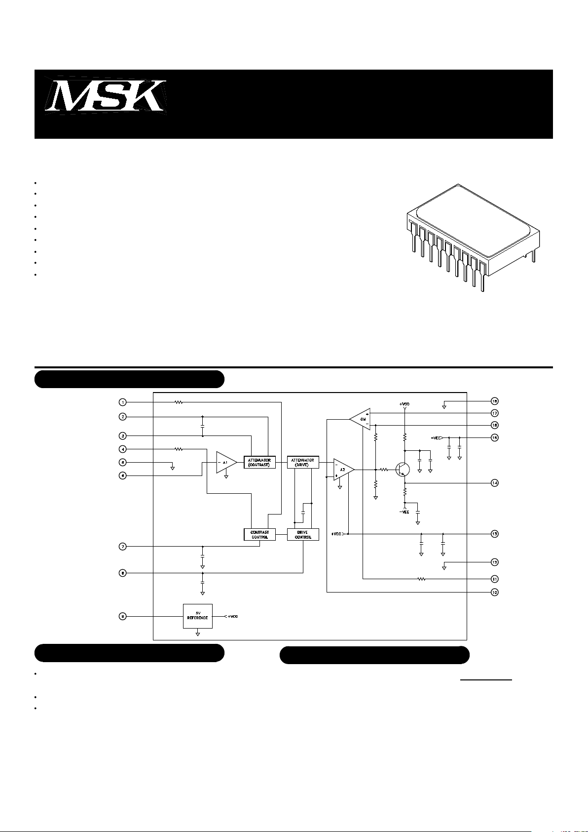
The MSK 621(B) is a very high frequency video amplifier system capable of driving displays with resolutions up to
1664 x 1200. Brightness is controlled with a gated differential input black level clamp comparator. There are also DC
inputs available for contrast control and drive control. All DC control inputs operate over a 0V to 4V input range and
feature high impedance inputs. In addition to all of the features offered in the MSK 620, the MSK 621 contains an
emitter follower buffer output stage which allows the device to easily drive video lines at greater current levels. The
MSK 621(B) is packaged in a space efficient hermetically sealed 18 pin dip package.
DESCRIPTION:
Clamp Cap
Clamp Gate Input
Ground
+Vcc
Video Output
-Vee
Clamp Input (-)
Clamp Input (+)
Ground
1
2
3
4
5
6
7
8
9
Control Output (+)
Attn. Input (+)
Attn. Input (-)
Control Output (-)
Ground
Video Input
Contrast Control Input
Drive Control Input
Vref Output
PIN-OUT INFORMATION
10
11
12
13
14
15
16
17
18
Wideband Amplifier With Gain
and DC Offset Control
High Resolution CRT Monitor
Ultra High Performance Video Processing
TYPICAL APPLICATIONS
EQUIVALENT SCHEMATIC
Rev. A 8/00
1
ISO 9001 CERTIFIED BY DSCC
RLOAD=∞; +VCC
VIN=N/C
Comparator Off
Comparator On
Clamp Cap Voltage = 0V
Clamp Cap Voltage = 6V
VCONTRAST=0.5V
fIN=12KHz
VDRIVE=0V to 4V
V0=4VPP
V0=4VPP
V0=4VPP
IL=0mA Ext
VCC=11V to 13V
IL=0 to 10mA
-55°C≤Tc≤125°C
STATIC
Power Supply Current
Video Input Bias Voltage
Clamp Gate High Input Voltage
Clamp Gate Low Input Voltage
DYNAMIC CHARACTERISTICS
Video Amplifier Gain
Video Output Low Voltage
Video Output High Voltage
Attenuation
Video Amplifier Input Resistance
Gain Range
-3dB Video Amplifier Bandwidth
Output Rise Time
Output Fall Time
VOLTAGE REFERENCE
Output Voltage
Line Regulation
Load Regulation
Output Voltage Change w/Temp.
+13.5V
-8V
19.0°C/W
Vcc≥Vin≥GND
100mA
20mA
1
2
3
4
5
6
-65°C to +150°C
300°C
-40°C to +85°C
-55°C to +125°C
150°C
ABSOLUTE MAXIMUM RATINGS
TST
TLD
TC
TJ
Storage Temperature Range
Lead Temperature Range
(10 Seconds)
Case Operating Temperature
MSK621
MSK621B
Junction Temperature
Supply Voltage
Supply Voltage
Thermal Resistance
(Junction to Case)
Voltage At Any Input Pin
Video Output Current
Reference Output Current
○○○○○○○○○○○○○
○○○○○○○○○○
+VCC
-VEE
θJC
VIN
IOUT
IOUTREF
RIN=30Ω, CIN=10µF, RL=499Ω, unless otherwise specified. Clamp Gate Input=0V, VCONTRAST=VDRIVE=VBRIGHTNESS=4V.
Guaranteed by design but not tested. Typical parameters are representative of actual device performance but are for reference only.
Industrial grade devices shall be tested to subgroups 1 and 4 unless otherwise specified.
Military grade devices ('B' suffix) shall be 100% tested to subgroups 1,2,3 and 4.
Subgroup 5 and 6 testing available upon request.
Subgroup 1,4 TA=TC=+25°C
Subgroup 2,5 TA=TC=+125°C
Subgroup 3,6 TA=TC=-55°C
○○○○○○○○○○○○
○○○○○○○○○○○○
○○○○○○○○○○○
NOTES:
Group A
Subgroup
1,2,3
1,2,3
1,2,3
1,2,3
4
4
4
-
-
4
4
4
4
1
-
-
-
Typ.
96
2.65
-
-
20
-0.2
10
-23
20
6
230
1.5
1.5
5.00
0.006
0.005
0.18
Min.
-
2.0
2.0
-
16
-
9.0
-
-
5
200
-
-
4.95
-
-
-
Max.
110
2.9
-
0.8
24
0.0
-
-
-
-
-
2.0
2.0
5.05
0.01
0.01
0.45
Min.
-
2.0
1.8
-
16
-
9.0
-
-
5
190
-
-
4.9
-
-
-
Max.
120
2.9
-
1.0
24
0.0
-
-
-
-
-
3.0
3.0
5.1
0.01
0.01
0.45
MSK 621B MSK 621
Parameter
Test Conditions
ELECTRICAL SPECIFICATIONS
+Vcc=+12.0V, -VEE=-5V Unless Otherwise Specified
1
mA
V
V
V
V/V
V
V
dB
KΩ
dB
MHz
nS
nS
V
%/V
%/mA
%
Units
2
5
5
2
5
5
5
Typ.
105
2.65
-
-
20
-0.2
10
-23
20
6
200
2.0
2.0
5.0
0.006
0.005
0.18
2
2
2
○○○○○○○○
○○○○○○○○○○
○○○○
○○○○○○○○○
○○○○○○○○○○○○○○○○
5
5
Rev. A 8/00
2
 Loading...