

MSK MSK604B, MSK604 Datasheet
ISO 9001 CERTIFIED BY DSCC
NEGATIVE OUTPUT
WIDE BANDWIDTH
M.S.KENNEDY CORP.
4707 Dey Road Liverpool, N.Y. 13088
HIGH VOLTAGE AMPLIFIER
FEATURES:
Negative Going Output Voltage
Ultra Low Quiescent Current - ±10mA for High Voltage
95V Peak to Peak Output Voltage Swing
Slew Rate - 3000V/µS Typical
Full Power Output Frequency - 2 MHz Typical
Output Current - 250mA Peak
Adjustable - VHV Power Supply Minimizes Power Dissipation
Compact Package Offers Superior Power Dissipation.
MIL-PRF-38534 QUALIFIED
DESCRIPTION:
The MSK 604(B) is a high voltage wideband amplifier designed to provide large negative voltage swings at high
slew rates in wideband systems. The true inverting op-amp topology employed in the MSK 604 provides excellent
D.C. specifications such as input offset voltage and input bias current. These attributes are important in amplifiers
that will be used in high gain configurations since the input error voltages will be multiplied by the system gain. The
MSK 604 achieves impressive slew rate specifications by employing a feed forward A.C. path through the amplifier;
however, the device is internally configured in inverting mode to utilize this benefit. Internal compensation for gains
of -5V/V or greater keeps the MSK 604 stable in this range. The MSK 604 is packaged in a space efficient,
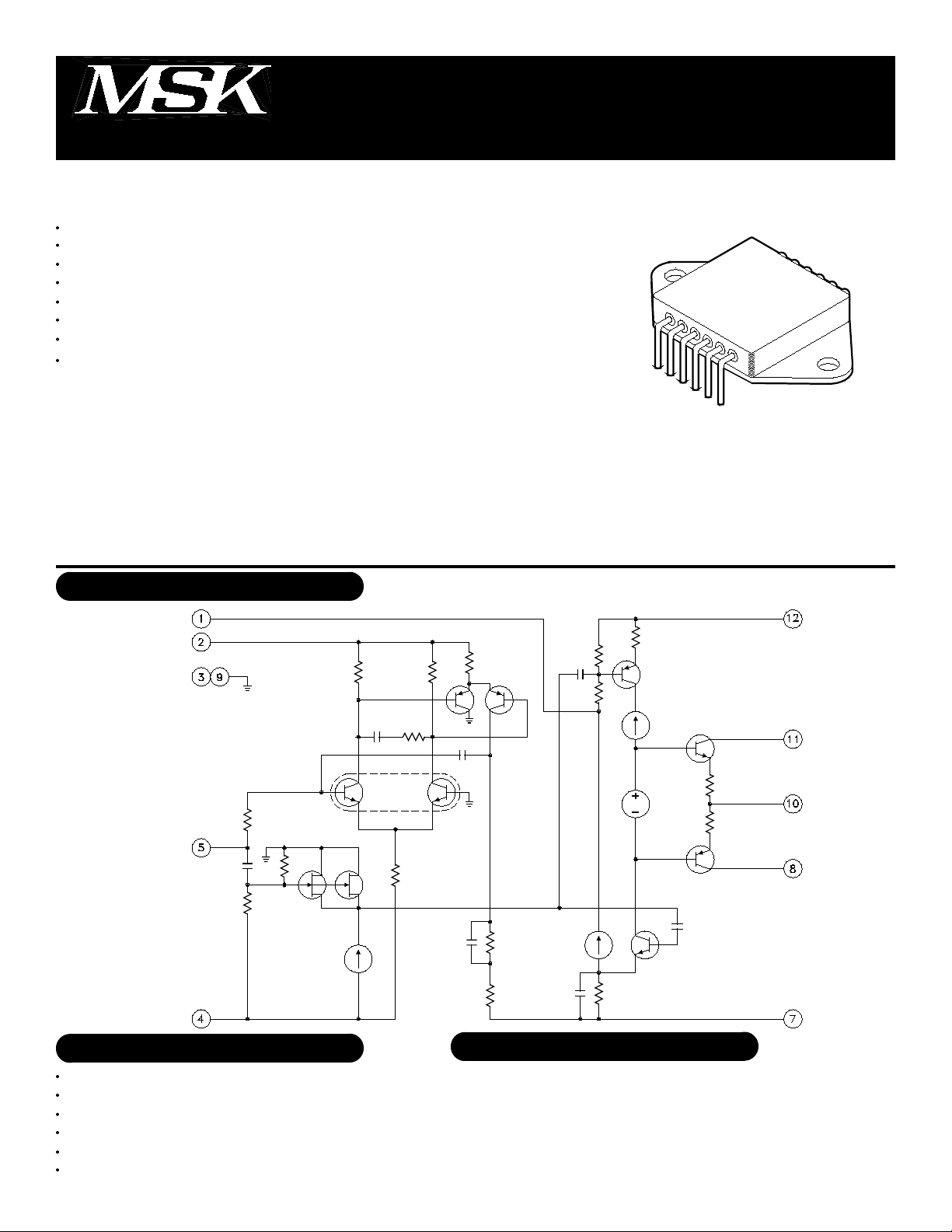
hermetically sealed, 12 pin power dual in line package that has a high thermal conductivity for efficient device cooling.
604
(315) 701-6751
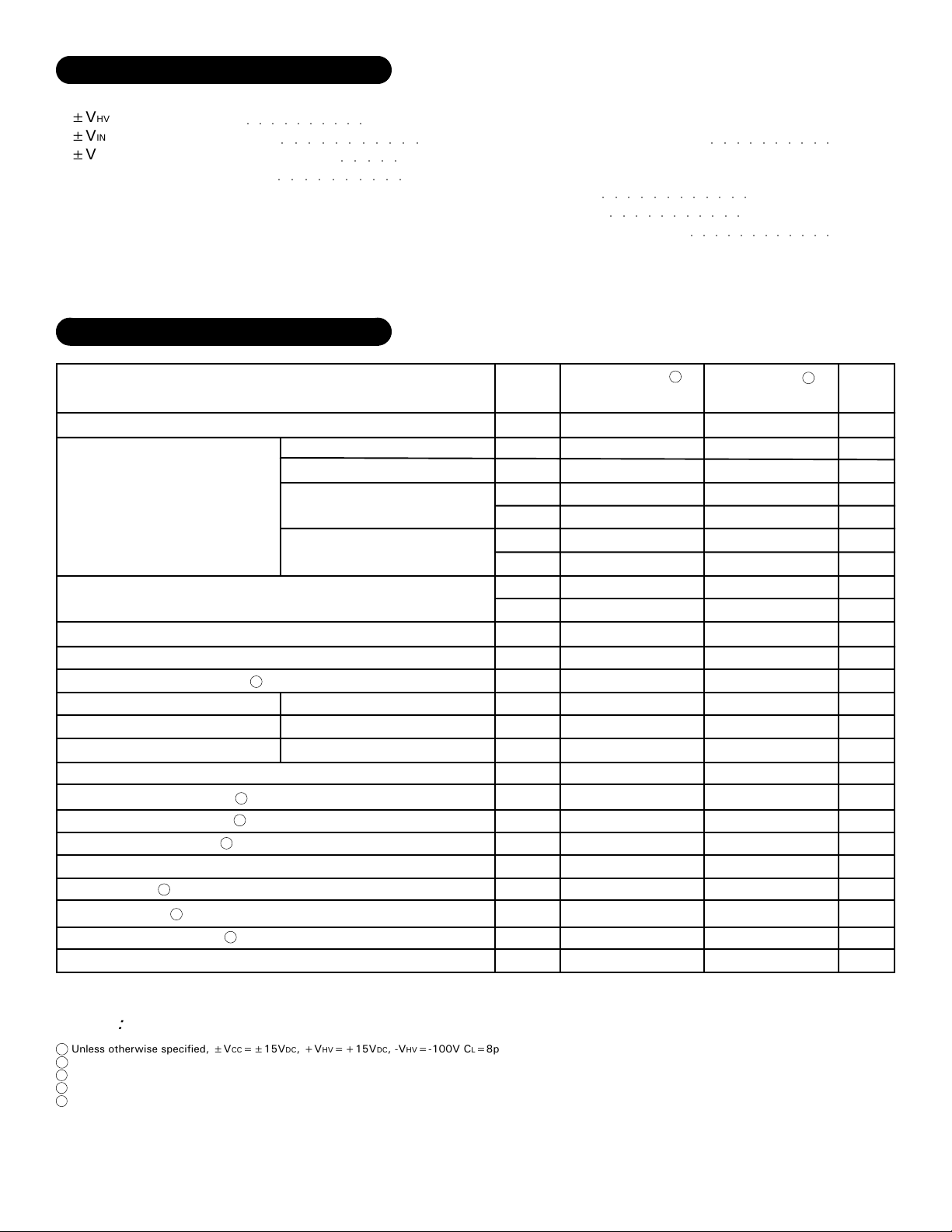
EQUIVALENT SCHEMATIC
TYPICAL APPLICATIONS
Wideband High Voltage Amplifier
High Resolution CRT Monitor Grid Drive
Ultra High Performance Video Processing
CRT Beam Intensity Control
Varactor Tuned VCO Driver
Automatic Test Equipment
PIN-OUT INFORMATION
1
COMP
2
+VCC
3
GROUND
4
-VCC
5
-INPUT
6
NO CONNECTION
1
12
+VHV
11
+VSC
10
OUTPUT
9
CASE/GROUND
8
-VSC
7
-VHV
Rev. B 8/00
ABSOLUTE MAXIMUM RATINGS
±VHV
±VIN
±VCC
θJC
Supply Voltage
Input Voltage Range
Supply Voltage (Input Stage)
Thermal Resistance
○○○○○○○○○○
○○○○○○○○○○○
○○○○○○○○○○
(Output Devices)
ELECTRICAL SPECIFICATIONS
Parameter
STATIC
Quiescent Current
Input Offset Voltage
Input Bias Current
Input Offset Voltage Drift
Power Supply Range
DYNAMIC CHARACTERISTICS
Output Voltage Swing
Peak Output Current
Full Power Output
Unity Gain Bandwidth
Slew Rate
Voltage Gain
2
2
Settling Time to 1%
Settling Time to 0.1%
2
2
2
2
2
+20,-120VDC
±VCC
○○○○○
±18VDC
18°C/W
Test Conditions
VIN=0 @ +VCC
VIN=0 @ -VCC
VIN=0 @ +VHV
VIN=0 @ -VHV
VIN=0
VIN=0
±VCC
+VHV
-VHV
f=1KHz
f=1KHz
VO=70V
VO=1.0V
VO=80V
f=1KHz
AV=-10V/V VO=50V
AV=-10V/V VO=50V
TST
Storage Temperature Range
TLD
Lead Temperature Range
(10 Seconds)
TC
Case Operating Temperature
MSK604
MSK604B
TJ
Junction Temperature
Group A
Subgroup
1,2,3
1,2,3
1
2,3
1
2,3
1
2,3
1
2,3
2,3
-
-
-
4
-
-
-
4
-
-
-
○○○○○○○○○○○○
○○○○○○○○○○○
MSK 604B MSK 604
Min.
Typ.
-
1.5
-
15
-
10
-
14
-
10
-
14
-
±1.0
-
±2.0
-
50
-
100
-
±10
±12
±15
0
+15
-50
-100
-90/+5
±100
1
50
2000
94
-
-
-95/8
±250
2
100
3000
100
200
1000
-65°C to +150°C
○○○○○○○○○○
-40°C to +85°C
-55°C to +125°C
○○○○○○○○○○○○
4
Max.
2.0
±5.0
±10.0
250
350
±50
±18
+20
-120
25
15
17
15
17
-
-
-
-
-
-
-
-
Min.
-
-
-
-
-
-
-
-
-
-
-
±12
0
-50
-90/+5
±100
1
50
2000
90
-
-
Typ.
±1.0
±2.0
±10
±15
+15
-100
-95/8
±250
3000
1000
1.8
20
10
-
10
-
50
100
2
100
100
200
3
Max.
2.5
30
20
-
20
-
±10
-
500
-
-
±18
+20
-120
-
-
-
-
-
-
-
-
300°C
150°C
Units
mA
mA
mA
mA
mA
mA
mV
mV
nA
nA
µV/°C
V
V
V
V
mA
MHz
MHz
V/µS
dB
nS
nS
NOTES:
1
Unless otherwise specified, ±VCC=±15VDC, +VHV=+15VDC, -VHV=-100V CL=8pF (probe capacitance) and AV=-10V/V.
2
This parameter is guaranteed by design but not tested. Typical parameters are representative of actual device performance but are for reference only.
3
Industrial grade devices shall be tested to subgroups 1 and 4 unless otherwise specified.
4
Military grade devices ('B' suffix) shall be 100% tested to subgroups 1,2,3 and 4.
5
Subgroup 1,4 TA=TC=+25°C
Subgroup 2,5 TA=TC=+125°C
Subgroup 3,6 TA=TC=-55°C
2
Rev. B 8/00
 Loading...