

MSK MSK5230-3.3, MSK5230-3.3H, MSK5230-5, MSK5230-2.5, MSK5230-12 Datasheet
...
4707 Dey Road Liverpool, N.Y. 13088
M.S.KENNEDY CORP.
(315) 701-6751
FEATURES:
SERIES
ISO-9001 CERTIFIED BY DSCC
Hermetic Surface Mount Package
Extremely Low Dropout Voltage: 370mV @ 5 Amps
Available in 2.5V, 3.3V, 5.0V and 12.0V
On Board Thermal Shut Down
Reverse Battery and Load Dump Protection
Low Ground Current: 70mA Typical at Full Load
1% Maximum Guaranteed Accuracy
Output Current to 5 Amps
Alternate Output Voltages Available
DESCRIPTION:
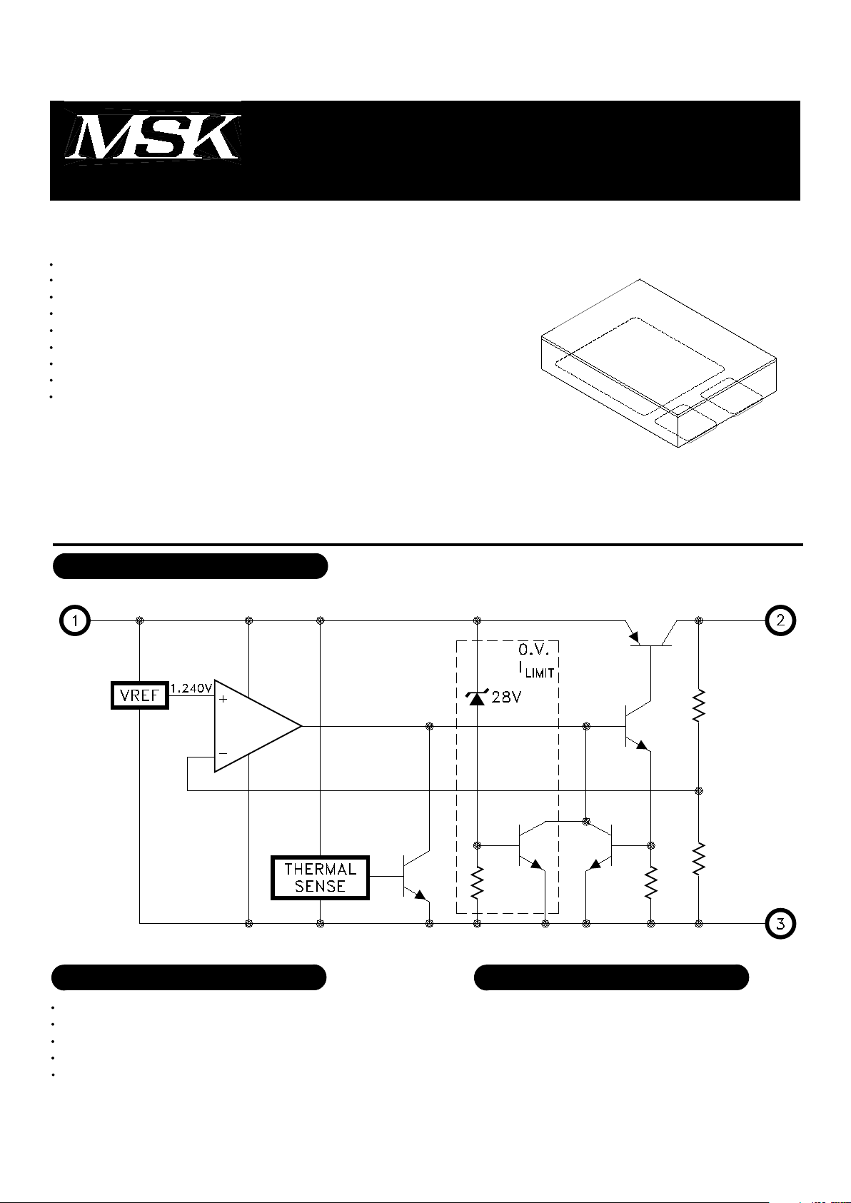
The MSK 5250 series voltage regulators are available in +2.5V, +3.3V, +5.0V, and +12.0V output configura-
tions. All boast ultra low dropout specifications due to the utilization of a super PNP output pass transistor with
monolithic technology. Dropout voltages of 370mV at 5 amps are typical in this configuration, which drives effi-
ciency up and power dissipation down. Accuracy is guaranteed with a 1% maximum output voltage tolerance. The
MSK 5250 series is packaged in a space efficient 3 pin power surface mount ceramic package.
EQUIVALENT SCHEMATIC
5250
TYPICAL APPLICATIONS
PIN-OUT INFORMATION
High Efficiency, High Current Linear Regulators
Constant Voltage/Current Regulators
System Power Supplies
Switching Power Supply Post Regulators
Battery Powered Equipment
VIN
VOUT
Ground
1
2
3
1 Rev. B 7/00
MIL-PRF-38534 QUALIFIED
VERY HIGH CURRENT, LOW DROPOUT
SURFACE MOUNT
VOLTAGE REGULATORS
Input Voltage (100mS 1%D.C.)
Input Voltage
Enable Voltage
Output Current
-20V to +60V
26V
-0.3V to 26V
5.5A
Storage Temperature Range . . -65°C to +150°C
Lead Temperature . . . . . . . ..........300°C
(10 Seconds Soldering)
Operating Temperature
MSK 5250 Series . . . . . . . . . -40°C to +85°C
MSK 5250H Series . . . . . . . -55°C to +125°C
VINP
VIN
VEN
IOUT
TST
TLD
TJ
ABSOLUTE MAXIMUM RATINGS
○○○○○○○○○○○○○○○
○○○○○○○○○○
○○○○○○○○○○○○○○○○
2 Rev. B 7/00
Output Current Limit 2
Output Noise 2
Thermal Resistance 2
Thermal Shutdown 2
∆VOUT = -1%; IOUT = 100 mA
∆VOUT = -1%; IOUT = 5A
VIN = VOUT+5V
10 mA ≤ IOUT ≤ 5A
(VOUT +1V) ≤ VIN ≤ 26V
IOUT = 10 mA
VOUT = 0V; VIN = VOUT +1V
VIN = VOUT +1V; IOUT = 2.5A
VIN = VOUT +1V; IOUT = 5A
CL = 20µF; 10 HZ ≤ f ≤ 100 KHZ
Junction to Case
TJ
Ground Current 2 8
1
2, 3
1
1
1
2, 3
1
2, 3
-
-
-
-
-
-
Parameter
ELECTRICAL SPECIFICATIONS
-
-
-
-
-
-
-
-
-
-
-
-
-
-
±0.5
±1.0
80
370
±0.2
±0.3
±0.05
±0.5
7.5
15
70
400
1.5
130
±1.0
±2.0
175
600
±1.0
±2.0
±0.5
±1.0
10
50
-
-
2.0
-
%
%
mV
mV
%
%
%
%
A
mA
mA
µV
°C/W
°C
-
-
-
-
-
-
-
-
-
-
-
-
-
-
±0.5
-
80
370
±0.2
±0.3
±0.05
±0.5
7.5
15
70
400
1.5
130
±1.0
-
200
625
±1.2
-
±0.6
-
10
55
-
-
2.2
-
Group A
Subgroup
MSK 5250H SERIES
Min. Typ. Max.
MSK 5250 SERIES
Min. Typ. Max.
Units
Test Conditions 1 3
Output Voltage Tolerance
Dropout Voltage 2
Load Regulation
Line Regulation
IOUT = 10mA; VIN = VOUT +1V
+2.5V
+3.3V
+5.0V
+12.0V
OUTPUT
VOLTAGE
7
PART
NUMBER
1
2
3
4
5
6
7
8
NOTES:
Output decoupled to ground using 20µF minimum capacitor unless otherwise specified.
This parameter is guaranteed by design but need not be tested.
Typical parameters are representative of actual device performance but are for reference only.
All output parameters are tested using a low duty cycle pulse to maintain TJ = TC.
Industrial grade devices shall be tested to subgroup 1 unless otherwise specified.
Military grade devices ('H' suffix) shall be 100% tested to subgroups 1,2,3.
Subgroup 1
Subgroup 2
Subgroup 3
Please consult the factory if alternate output voltages are required.
The MSK 5250-2.5 has an additional 10 mA of Quiescent Current.
TC = +25°C
TJ = +125°C
TA = -55°C
MSK5250-2.5
MSK5250-3.3
MSK5250-5.0
MSK5250-12
 Loading...