

MSK MSK5100-5, MSK5100-00, MSK5100-12, MSK5100-12B, MSK5100-3.3 Datasheet
...
4707 Dey Road Liverpool, N.Y. 13088
M.S.KENNEDY CORP.
(315) 701-6751
FEATURES:
5100
SERIES
ISO-9001 CERTIFIED BY DSCC
HIGH CURRENT,
LOW DROPOUT
VOLTAGE REGULATORS
Extremely Compact 10 Pin SOIC With Heat Sink Tab
Extremely Low Dropout Voltage: 350mV @ 1.5 Amps
Available in 3.3V, 5.0V, 12.0V and Adjustable Versions
Open Collector Error Flag Output
TTL Level Enable Pin: Zero Current Shutdown Mode
Reverse Battery and Load Dump Protection
Low Ground Current: 22mA Typical at Full Load
1% Guaranteed Accuracy
Output Current to 1.5 Amps
MIL-PRF-38534 QUALIFIED
DESCRIPTION:
The MSK 5100 series voltage regulators are available in +3.3V, +5.0V, +12.0V or adjustable output configura-
tions. All boast ultra low dropout specifications due to the utilization of a super PNP output pass transistor with
monolithic technology. Dropout voltages of 350mV at 1.5 amps are typical in this configuration, which drives effi-
ciency up and power dissipation down. Accuracy is guaranteed with a 1% output voltage tolerance. The series also
offers a TTL/CMOS compatible on/off enable function as well as an output flag pin. The MSK 5100 series is packaged
in a space efficient 10 pin power SOIC with a built in copper-moly sink tab.
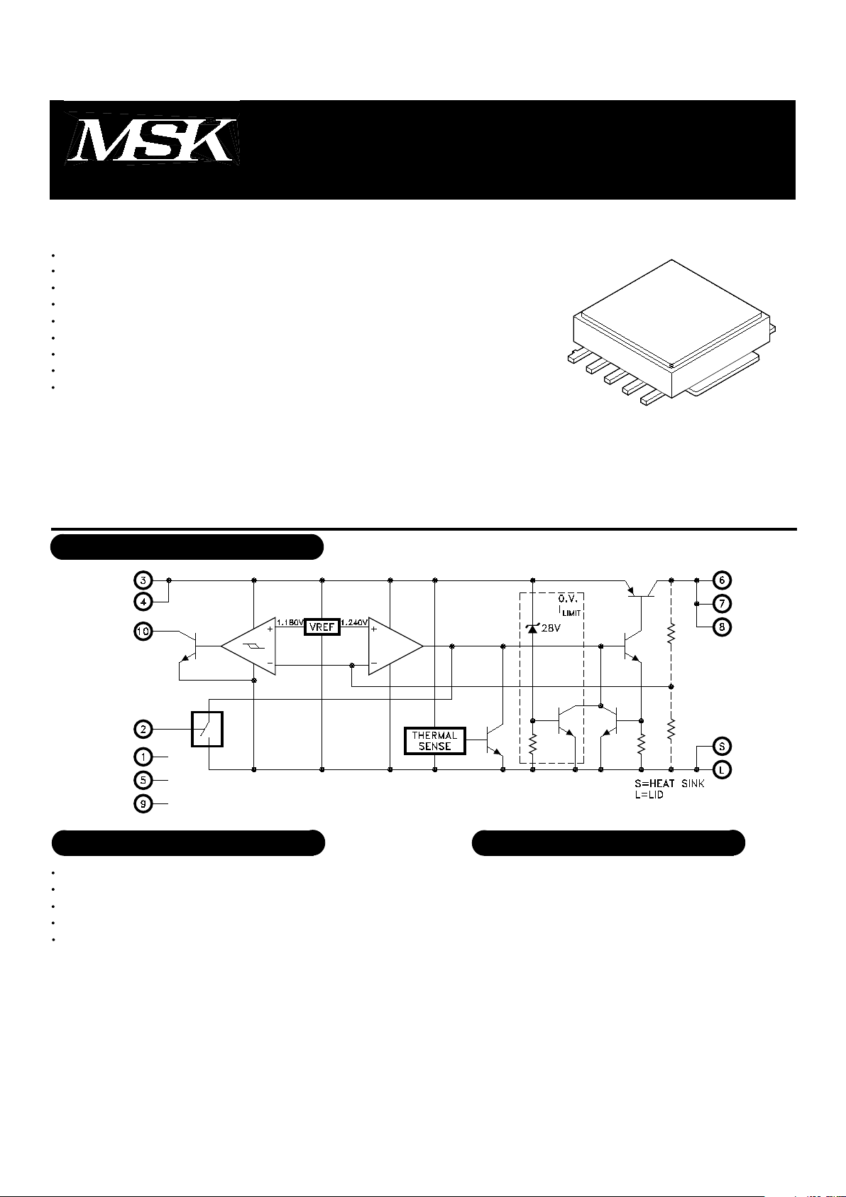
EQUIVALENT SCHEMATIC
TYPICAL APPLICATIONS
PIN-OUT INFORMATION
High Efficiency, High Current Linear Regulators
Constant Voltage/Current Regulators
System Power Supplies
Switching Power Supply Post Regulators
Battery Powered Equipment
N/C
Enable
Vin A
Vin B
N/C
Vout A
Vout B
N/C
Adj
N/C
1
2
3
4
5
6
7
8
9
10
MSK5100-00
N/C
Enable
Vin A
Vin B
N/C
Vout A
Vout B
Vout C
N/C
Flag
1
2
3
4
5
6
7
8
9
10
MSK5100-3.3,-5.0,-12
HEAT SINK
The heat sink of the package and the
lid are electrically connected to ground.
Schematic shown for fixed output voltage versions
Rev. D 10/00
1
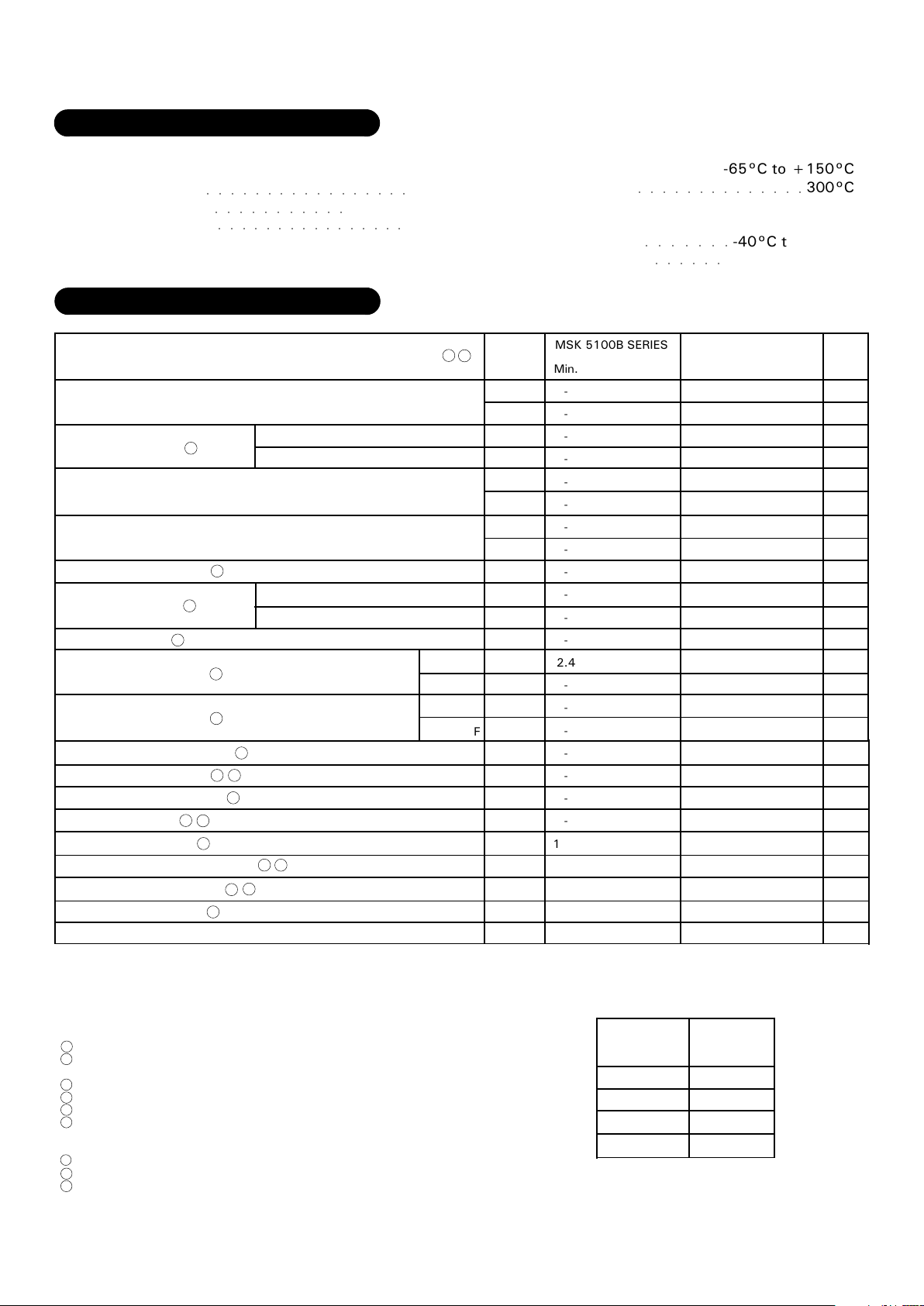
Output Voltage Tolerance
Dropout Voltage
Load Regulation
Line Regulation
Ground Current
Enable Input Voltage
Enable Input Current
Output Current Limit
Output Noise
Shutdown Output Current
Flag Output Leakage
Flag Output On Voltage
Flag Threshold
Reference Voltage
Reference Voltage Temp Drift
Adjust Pin Bias Current
Thermal Resistance
Thermal Shutdown
Input Voltage (100mS 1%D.C.)
Input Voltage
Enable Voltage
Output Current
Storage Temperature Range
Lead Temperature
(10 Seconds Soldering)
Operating Temperature
MSK5100 Series
MSK5100B Series
Group A
Subgroup
1
2,3
1
1
1
2,3
1
2,3
-
-
-
-
1
1
1
1
-
-
1
-
1
-
-
-
-
%
%
mV
mV
%
%
%
%
A
mA
mA
µV
V
V
µA
µA
µA
µA
V
mV
V
ppm/°C
nA
°C/W
°C
∆VOUT=-1%; IOUT=100m A
∆VOUT=-1%; IOUT=1.5A
VIN=VOUT+5V
10mA ≤ IOUT ≤ 1.5A
(VOUT +1V) ≤ VIN ≤ 26V
IOUT=10mA
VOUT=0V; VIN=VOUT+1V
VIN=VOUT+1V; IOUT=0.75A
VIN=VOUT+1V; IOUT=1.5A
CL=10µF; 10Hz ≤ f ≤ 100KHz
VENABLE ≤ 0.8V
VOH=26V
IOL ≤ 250µA; VIN=VOUT-2V
VIN=VOUT-7%
Normal Operation
Normal Operation
Full Temp; VIN=VOUT+1V
Junction to Case
TJ
-20V to +60V
26V
-0.3V to 26V
3.5A
Adjustable
+3.3V
+5.0V
+12.0V
VINP
VIN
VEN
IOUT
Parameter
TST
TLD
TJ
ELECTRICAL SPECIFICATIONS
ABSOLUTE MAXIMUM RATINGS
○○○○○○○○○○○○○○
○○○○○○○
○○○○○○
-65°C to +150°C
300°C
-40°C to +85°C
-55°C to +125°C
1
Test Conditions
1
2
3
4
5
6
7
8
9
NOTES:
Output decoupled to ground using 10µF minimum capacitor unless otherwise specified.
This parameter is guaranteed by design but need not be tested.
Typical parameters are representative of actual device performance but are for reference only.
All output parameters are tested using a low duty cycle pulse to maintain TJ = TC.
Industrial grade devices shall be tested to subgroups 1 and 4 unless otherwise specified.
Military grade devices ('B' suffix) shall be 100% tested to subgroups 1,2,3 and 4..
Subgroup 1,4
Subgroup 2
Subgroup 3
Please consult the factory if alternate output voltages are required.
Applies to MSK5100-00 adjustable version only.
Applies to fixed output devices only.
PART
NUMBER
OUTPUT
VOLTAGE
TC=+25°C
TJ=+125°C
TA=-55°C
MSK5100-00
MSK5100-3.3
MSK5100-5.0
MSK5100-12
○○○○○○○○○○○○○○○○
○○○○○○○○○○○
○○○○○○○○○○○○○○○○○
HIGH/ON
LOW/OFF
HIGH/ON
LOW/OFF
MSK 5100B SERIES
Min.
-
-
-
-
-
-
-
-
-
-
-
-
2.4
-
-
-
-
-
-
-
1.22
-
-
-
-
Typ.
±0.5
±1.0
80
350
±0.2
±0.3
±0.05
±0.5
2.1
8
22
400
-
-
20
1
10
0.01
0.2
75
1.24
20
40
1.8
130
Max.
±1.0
±2.0
200
600
±1.0
±2.0
±0.5
±1.0
3.5
20
-
-
-
0.8
75
2
20
2
0.4
-
1.26
-
120
2
-
Typ.
±0.5
-
80
350
±0.2
±0.3
±0.05
±0.5
2.1
8
22
400
-
-
20
1
10
0.01
0.2
75
1.24
20
40
1.8
130
MSK 5100 SERIES
Min.
-
-
-
-
-
-
-
-
-
-
-
-
2.4
-
-
-
-
-
-
-
1.22
-
-
-
-
Max.
±1.0
-
225
625
±1.2
-
±0.6
-
3.5
20
-
-
-
0.8
75
2
20
2
0.4
-
1.26
-
150
2
-
Units
2
2
2
2
8
2 8
8
2
9
9
2 9
2
3
IOUT=1A; VIN=VOUT+1V
2
Rev. D 10/00
2
2
2
2
 Loading...