

MSK MSK5042H, MSK5042, MSK5042E Datasheet
M.S.KENNEDY CORP.
ISO-9001 CERTIFIED BY DSCC
HIGH EFFICIENCY,
4 AMP ADJUSTABLE
SURFACE MOUNT
SWITCHING REGULATOR
5042
4707 Dey Road Liverpool, N.Y. 13088
FEATURES:
Up To 95% Efficiency For 5V Operation
4 Amp Output Current
4.5V to 30V Input Range
User Adjustable Output Voltage from 1.2V to 5.5V
300KHz Switching Frequency @ 1 Amp
User Programmable Soft-Start
Quiescent Current < 2.5mA
User Programmable Current Limit
MIL-PRF-38534 QUALIFIED
(315) 701-6751
DESCRIPTION:
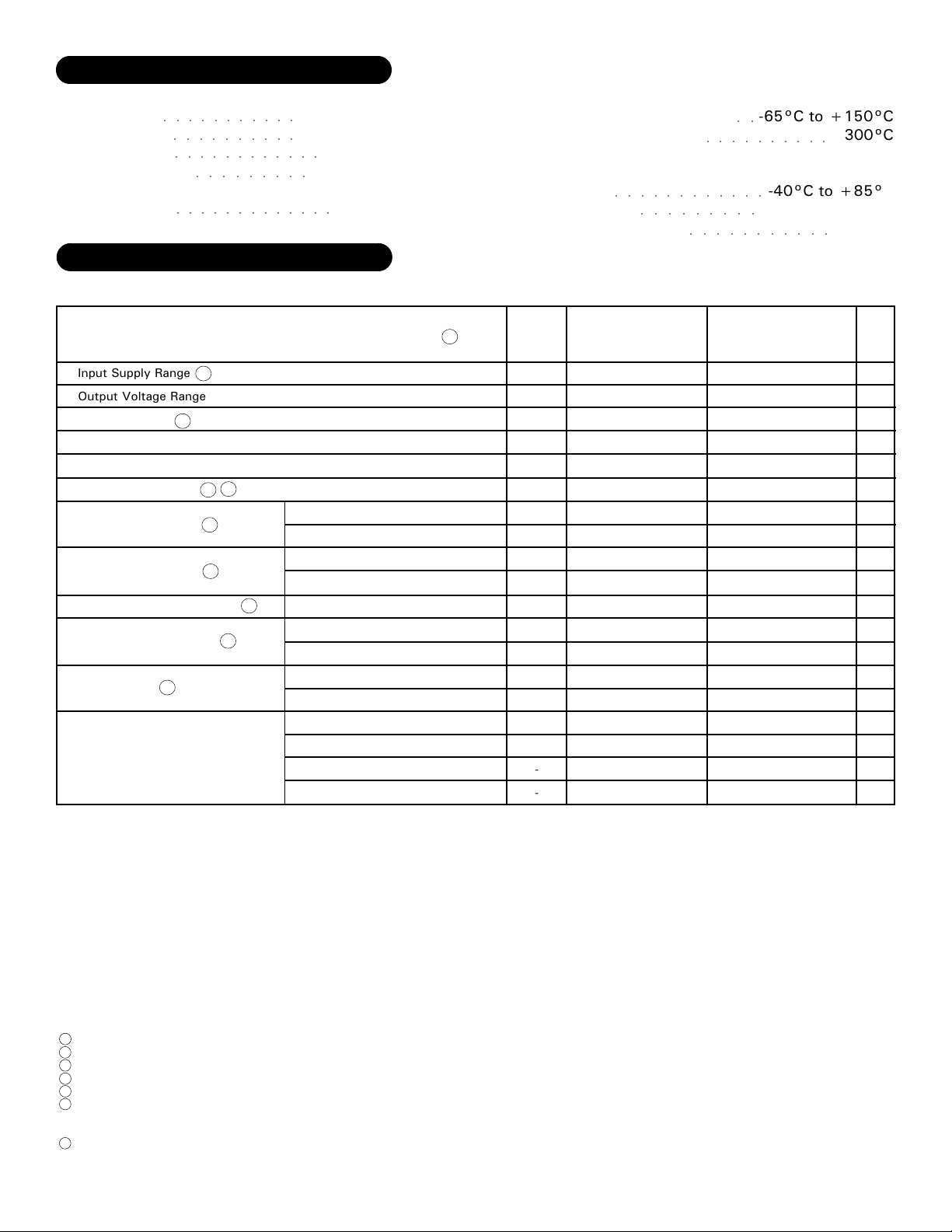
The MSK 5042 is a high efficiency, 4 amp, surface mount switching regulator. Output voltage is user adjustable
through the use of two external resistors or one external potentiometer. Output voltages from 1.2 volts to 5.5 volts
are possible. The operating frequency of the MSK 5042 is 300KHz and is internally set. An external "soft start"
capacitor allows the user to control how quickly the output comes up to regulation voltage after the application of an
input. An extremely low quiescent current of typically less than 2.5mA and nearly 95% operating efficiency at 5 volts
out, keep the total internal power dissipation of the MSK 5042 down to an absolute minimum.
EQUIVALENT SCHEMATIC
TYPICAL APPLICATIONS
Step-down Switching Regulator
Microprocessor Power Source
High Efficiency Low Voltage
Subsystem Power Supply
PIN-OUT INFORMATION
Case
1
Sense High
2
Sense Low
3
N/C
4
RF High
5
Amp In
6
N/C
7
34-44
23-33
11-22
10
9
8
PRELIMINARY Rev. B 1/021
Vout
Ground
Vin
Enable
Ref Out
Cton
ABSOLUTE MAXIMUM RATINGS
Input Voltage
Enable Voltage
Output Current
Sense Pin Voltage
○○○○○○○○○○○
○○○○○○○○○○
○○○○○○○○○○○○
○○○○○○○○○
Thermal Resistance
(Each MOSFET)
○○○○○○○○○○○○○
ELECTRICAL SPECIFICATIONS
Parameter
Input Supply Range
Output Voltage Range
Output Current
Load Regulation
Line Regulation
Oscillator Frequency
Enable Input Voltage
Enable Input Current
Disabled Quiescent Current
Current Limit Threshold
Cton Current
Efficiency
2
2
2
2
7
2
2
2
2
-0.3V, +36V
-0.3V, +36V
TST
TLD
5.0 Amps
-0.3V, +7V
TC
17°C/W
TJ
Test Conditions
IOUT=1.5A VIN=6.5V
Within SOA
0.75A≤IOUT≤2.5A
IOUT=1A 6.5V≤VIN≤20V
Internal IOUT≥1.5A
High
Low
VEN=VIN
VEN=0V
VEN=0V VIN=30V
Positive
Negative
Source
Fault Sink
VIN=5.0V IOUT=1.5A VOUT=1.9V
VIN=5.0V IOUT=1.5A VOUT=2.5V
VIN=5.0V IOUT=1.5A VOUT=3.3V
VIN=6V IOUT=1A VOUT=5V
1
Storage Temperature Range
Lead Temperature Range
(10 Seconds)
Case Operating Temperature
MSK5042
MSK5042H/E
○○○○○○○○○○○○
○○○○○○○○○
Junction Temperature
Group A
Subgroup
1,2,3
1
1
-
1,2,3
-
1,2,3
1,2,3
1
1
1
1
1
1
1
-
-
-
-
MSK 5042 H/E
Min. Typ.
4.75
1.2
4.0
-
-
270
2.0
-
-
-
-
80
-50
2.5
2.0
-
-
-
-
-
-
4.5
1.5
0.06
300
-
-
0.5
0.2
2.0
100
-100
4.0
-
70
80
90
95
Max.
30
5.5
0.10
330
0.5
2.0
2.0
2.5
120
-160
6.5
-65°C to +150°C
○○
○○○○○○○○○○
-40°C to +85°C
-55°C to +125°C
○○○○○○○○○○○
MSK 5042
Min.
Typ.
4.75
1.2
-
4.0
-
-
-
270
-
2.0
-
-
-
-
75
-45
2.5
-
2.0
-
-
-
-
-
-
-
-
Max.
-
-
4.5
1.5
0.06
300
-
-
0.5
0.2
2.0
100
-100
4.0
-
70
80
90
95
300°C
+150°C
Units
30
5.5
-
-
%/V
0.15
KHz
330
-
0.5
2.0
2.0
2.5
125
-165
6.5
-
-
-
-
-
V
V
A
%
V
V
µA
µA
mA
mV
mV
µA
mA
%
%
%
%
NOTES:
1
VIN=Enable, 5mV≤(sense high-sense low)≤75mV, IL=0A, COUT=6x330µF, CIN=6x220µF, CTON=0.01µF unless otherwise specified.
2
This parameter is guaranteed by design but need not be tested. Typical parameters are representative of actual device performance but are for reference only.
3
All output parameters are tested using a low duty cycle pulse to maintain TJ = TC.
4
Industrial grade and 'E' suffix devices shall be tested to subgroup 1 unless otherwise specified.
5
Military grade devices ('H' suffix) shall be 100% tested to subgroups 1,2 and 3.
6
Subgroup 1
Subgroup 2
Subgroup 3
7
Actual switching frequency can be load dependent if output current is low. Refer to typical performance curves.
TA=TC=+25°C
TA=TC=+125°C
TA=TC=-55°C
2
PRELIMINARY Rev. B 1/02
 Loading...