

MSK MSK5021, MSK5021B Datasheet
M.S.KENNEDY CORP.
ISO-9001 CERTIFIED BY DSCC
HIGH CURRENT,
SUPER LOW DROPOUT
ADJUSTABLE VOLTAGE REGULATOR
5021
4707 Dey Road Liverpool, N.Y. 13088
FEATURES:
Extremely Low Dropout Voltage: 0.50V @ 20 Amps
Output Voltage Adjustable from 1.3V to 36V with Two External Resistors
TTL Level Enable Pin
Externally Programmable Current Limit
Low Quiescent Current
Available Fully Qualified to Mil-PRF-38534
Output Current to 20 Amps
Regulation Dropout Fault Pin
MIL-PRF-38534 CERTIFIED
(315) 701-6751
DESCRIPTION:
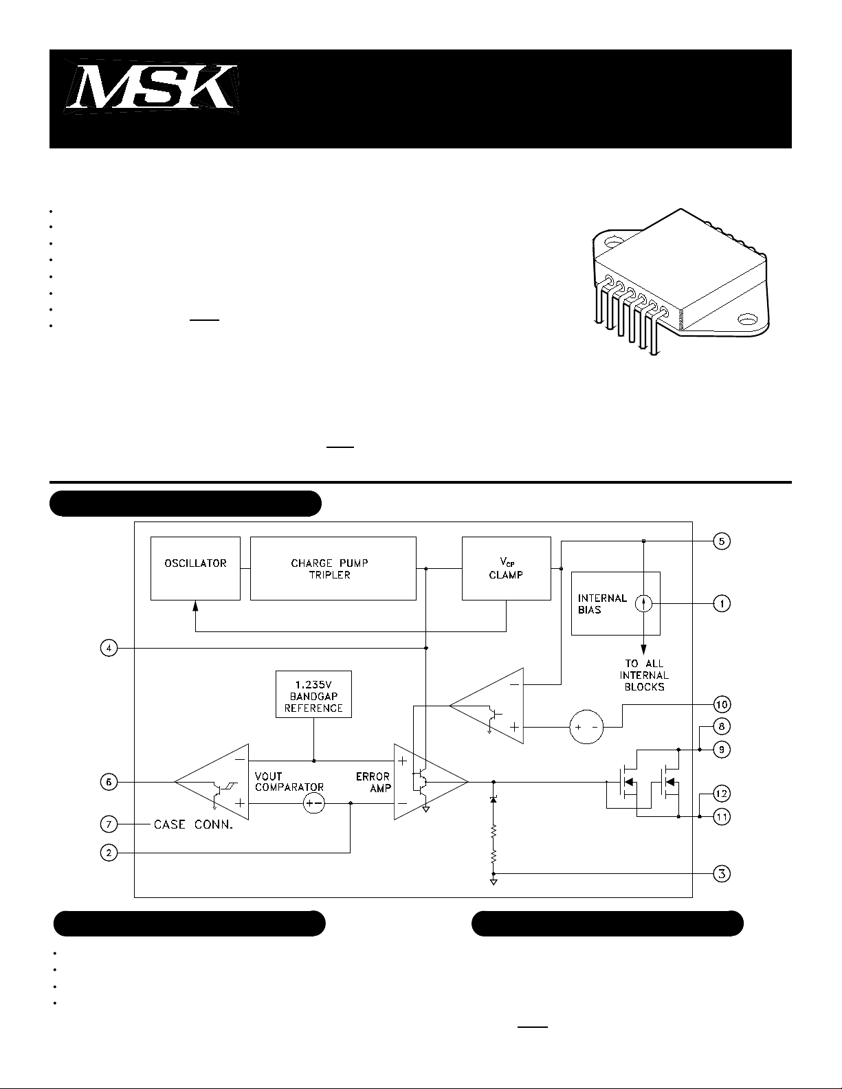
The MSK 5021 is a user adjustable voltage regulator capable of delivering 20 amps to a load with only a 0.5 volt
dropout voltage rating. The output voltage is adjustable from 1.3 volts to 36 volts through the selection of two
external resistors. Low dropout voltage ratings are achieved by employing a unique parallel MOSFET output pass
transistor configuration which drives power dissipation down and efficiency up. Accuracy is guaranteed with a ±1%
voltage tolerance at room temperature that only varies ±2% over temperature. A TTL level can be used to enable/
disable the device and a regulation dropout fault pin provides a means of monitoring the output level. The MSK 5021
is packaged in a thermally efficient 12 pin power dip that can be bolted directly to a heat sink.
EQUIVALENT SCHEMATIC
TYPICAL APPLICATIONS
High Efficiency, High Current Linear Regulators
Adjustable Voltage/Current Regulators
System Power Supplies
Switching Power Supply Post Regulators
PIN-OUT INFORMATION
12
1
Enable
2
VAdjust
3
Ground
4
CPump
5
Input
6
Fault
1
Output
11
Output
10
Sense
9
VSC
8
VSC
7
Case Connection
Rev. B 7/00
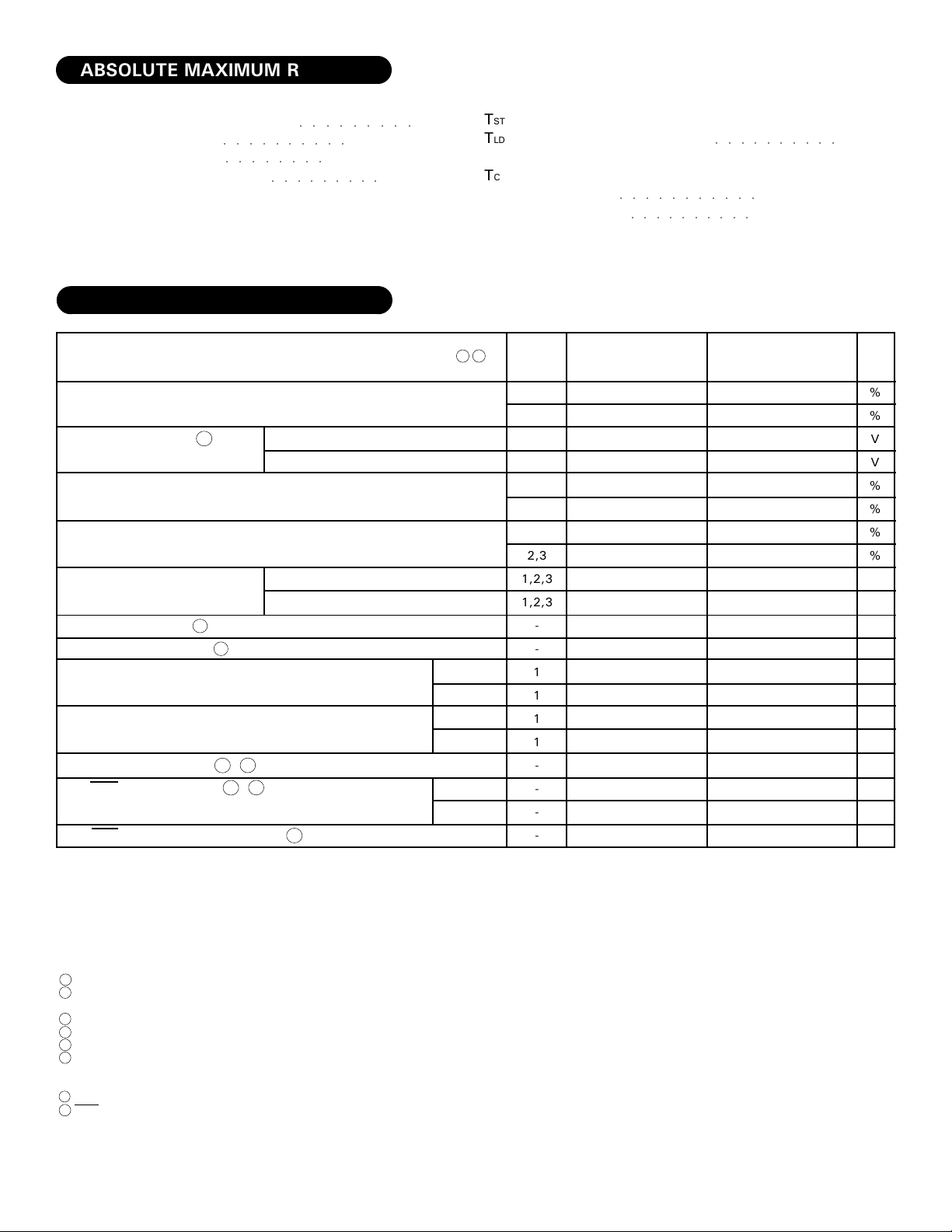
ABSOLUTE MAXIMUM RATINGS
Input Voltage (WRT VOUT)
VIN
Enable Voltage
VEN
Output Current
IOUT
Junction Temperature
TJ
○○○○○○○○○○
○○○○○○○○
○○○○○○○○○
20A within SOA
○○○○○○○○○
ELECTRICAL SPECIFICATIONS
36V
-0.3V to 36V
+175°C
TST
Storage Temperature Range
TLD
Lead Temperature Range
(10 Seconds)
TC
Case Operating Temperature
MSK5021
MSK5021B
○○○○○○○○○○○
○○○○○○○○○○
-65°C to +150°C
○○○○○○○○○○
-40°C to +85°C
-55°C to +125°C
300°C
Parameter
Output Voltage Tolerance
Dropout Voltage
2
Load Regulation
Line Regulation
Quiescent Current
Ripple Rejection 2
Thermal Resistance 2
Enable Input Voltage
Enable Input Current
2
Output Settling Time
Fault Output Voltage
7
2 8
Fault Output Sink Current Range
Test Conditions
1
IOUT=0A; VIN=VOUT+3V
IOUT= 0A
IOUT=20A
VIN=VOUT+3V
0A ≤ IOUT ≤ 20A
(VOUT +1.5V) ≤ VIN ≤ (VOUT+15V)
IOUT=0A
VEN=5V; VIN=VOUT+3V; IOUT=0A
VEN=0V; VIN=VOUT+3V; IOUT=0A
f=120Hz
Junction to Case
HIGH
LOW
HIGH
LOW
To within 10mV (IOUT=0A)
IFAULT=1mA
HIGH
LOW
2
3
Group A
Subgroup
1
2,3
1
1
1
2,3
1
2,3
1,2,3
1,2,3
-
-
1
1
1
1
-
-
-
-
MSK 5021(B)
Min.
Typ.
-
±0.5
-
±1.0
-
0.002
-
0.50
-
±0.5
-
±0.5
-
±0.5
-
±0.5
-
-
-
-
2.4
-
-
-
-
-
-
0.09
1
20
10
45
0.5
1.2
1.2
20
10
0.5
VIN
MSK 5021
2.4
1
Typ.
±0.5
-
-
-
-
-
-
-
-
-
-
-
-
-
0.002
0.5
±0.5
-
±0.5
-
20
10
45
0.5
1.2
1.2
-
20
-
10
-
0.5
-
VIN
-
0.09
-
-
Max.
Min.
±1.0
±2.0
0.010
0.75
±1.0
±2.0
±1.0
±1.0
30
50
-
0.6
-
0.8
50
25
-
-
-
10
-
Max.
±1.0
-
0.010
1.0
±1.0
-
±1.0
-
30
50
-
0.6
-
0.8
50
25
-
-
-
10
Units
%
%
V
V
%
%
%
%
mA
µA
dB
°C/W
V
V
µA
µA
mS
V
V
mA
NOTES:
Output decoupled to ground using 33µF minimum capacitor and RSC=0Ω unless otherwise specified.
1
This parameter is guaranteed by design but need not be tested. Typical parameters are representative of
2
actual device performance but are for reference only.
All output parameters are tested using a low duty cycle pulse to maintain TJ = TC.
3
Industrial grade devices shall be tested to subgroup 1 only unless otherwise specified.
4
Military grade devices ('B' suffix) shall be 100% tested to subgroups 1,2 and 3.
5
Subgroup 1
6
Subgroup 2
Subgroup 3
After application of enable pulse.
7
Fault pin connected to VIN through a 5.1KΩ resistor for VIN=5.0V.
8
TA=TC=+25°C
TA=TC=+125°C
TC=TC=-55°C
2
Rev. B 7/00
 Loading...