

MSK MSK5010-5TS, MSK5010-5TU, MSK5010-5ZD, MSK5010-5BZU, MSK5010-12BZD Datasheet
...
4707 Dey Road Liverpool, N.Y. 13088
M.S.KENNEDY CORP.
(315) 701-6751
FEATURES:
5010
SERIES
ISO-9001 CERTIFIED BY DSCC
HIGH CURRENT,
SUPER LOW DROPOUT
FIXED VOLTAGE REGULATORS
Extremely Low Dropout Voltage 0.45V @ 10 Amps
Available in 3.3V, 5.0V and 12.0V versions
Output Voltages Are Internally Set to ±1.5% maximum
TTL Level Enable Pin
Electrically Isolated Case
Low Quiescent Current
Output Current to 10 Amps
Available in Two Package Styles
Available with Three Lead Form Options
TYPICAL APPLICATIONS
High Efficiency, High Current Linear Regulators
Constant Voltage/Current Regulators
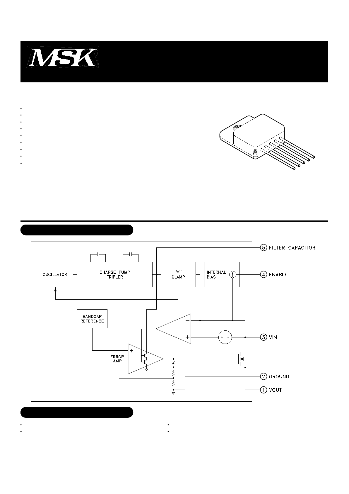
EQUIVALENT SCHEMATIC
MIL-PRF-38534 QUALIFIED
DESCRIPTION:
The MSK 5010 series voltage regulators are available in a +3.3V, +5.0V or +12.0V fixed output configuration.
All three boast ultra low dropout specifications due to the utilization of a MOSFET output pass transistor with
extremely low Rds(on). Dropout voltages of 0.45V at 10 amps are typical, in this configuration, which drives
efficiency up and power dissipation down. Accuracy is guaranteed with a 1.5% maximum initial output voltage
tolerance that varies only ±2% with temperature. The MSK 5010 series is packaged in a space efficient 5 pin SIP
that is electrically isolated from the internal circuitry allowing direct heat sinking for maximum heat dissipation.
1
Rev. F 7/00
System Power Supplies
Switching Power Supply Post Regulators
PART 7
NUMBER
IOUT=100mA; VIN=VOUT+3V
IOUT= 0A
IOUT=10A
VIN=VOUT+3V
100mA ≤ IOUT ≤ 9A
(VOUT +1.5V) ≤ VIN ≤ (VOUT+15V)
IOUT=100mA
VEN=VIN; VIN=VOUT+3V; IOUT=0A
VEN=0V; VIN=VOUT+3V; IOUT=0A
f=120Hz
Junction to Case
To within 10mV
Output Voltage Tolerance
Dropout Voltage 2
Load Regulation
Line Regulation
Quiescent Current
Ripple Rejection 2
Thermal Resistance 2
Enable Input Voltage 2
Enable Input Current 2
Output Settling Time 2 8
HIGH
LOW
HIGH
LOW
VIN
VEN
IOUT
TJ
Parameter
MSK 5010 SERIES
MSK 5010(B) SERIES
Input Voltage (WRT VOUT)
Enable Voltage
Output Current
Junction Temperature
○○○○○○○○○
○○○○○○○○
○○○○○○○○○
36V
-0.3V to 36V
10A within SOA
+175°C
TST
TLD
TC
Storage Temperature Range
Lead Temperature Range
(10 Seconds)
Case Operating Temperature
ELECTRICAL SPECIFICATIONS
ABSOLUTE MAXIMUM RATINGS
○○○○○○○○○○
-65°C to +150°C
300°C
-55°C to +125°C
3
Test Conditions
1
2
3
4
5
6
7
8
NOTES:
Output decoupled to ground using 20µF minimum capacitor unless otherwise specified.
This parameter is guaranteed by design but need not be tested.
Typical parameters are representative of actual device performance but are for
reference only.
All output parameters are tested using a low duty cycle pulse to maintain TJ = TC.
Industrial grade devices shall be tested to subgroup 1 unless otherwise specified.
Military grade devices ('B' suffix) shall be 100% tested to subgroups 1,2 and 3.
Subgroup 1
Subgroup 2
Subgroup 3
Please consult the factory if alternate output voltages are required.
After application of enable pulse
+12.0V
MSK5010-3.3
MSK5010-5.0
MSK5010-12
+3.3V
+5.0V
OUTPUT
VOLTAGE
○○○○○○○○○○
TA=TC=+25°C
TA=TC=+125°C
TA=TC= -55°C
Group A
Subgroup
1
2,3
1
1
1
2,3
1
2,3
1,2,3
1,2,3
-
-
1
1
1
1
-
Min.
-
-
-
-
-
-
-
-
-
-
-
-
2.4
-
-
-
-
Typ.
±0.3
±1.0
0.002
0.45
±0.5
±0.5
±0.3
±0.5
4.5
0.15
45
0.7
1.2
1.2
12.5
0.8
5
Max.
±1.5
±2.0
0.010
0.75
±1.0
±2.0
±1.0
±1.0
10
5.0
-
0.8
-
0.8
50
25
-
Min.
-
-
-
-
-
-
-
-
-
-
-
-
2.4
-
-
-
-
Typ.
±0.5
-
0.002
0.5
±0.5
-
±0.5
-
4.5
0.15
45
0.7
1.2
1.2
20
10
5
Max.
±1.5
-
0.015
1.0
±1.5
-
±1.5
-
10
5.0
-
1.0
-
0.8
50
25
-
Units
%
%
V
V
%
%
%
%
mA
µA
dB
°C/W
V
V
µA
µA
µS
2
2
Rev. F 7/00
 Loading...