

MSK MSK4364E, MSK4364H, MSK4364 Datasheet
ISO 9001 CERTIFIED BY DSCC
5 AMP, 55V, 3 PHASE
MOSFET BRUSHLESS
M.S.KENNEDY CORP.
4707 Dey Road Liverpool, N.Y. 13088 (315) 701-6751
FEATURES:
55 Volt Motor Supply Voltage
5 Amp Output Switch Capability
100% Duty Cycle High Side Conduction Capable
Shoot-Through/Cross Conduction Protection
Hall Sensing and Commutation Circuitry on Board
"Real" Four Quadrant Torque Control Capability
Good Accuracy Around the Null Torque Point
Isolated Design for High Voltage Isolation Plus Good Thermal Transfer
60°/ 120º Phasing Selectable
MOTOR CONTROLLER
MIL-PRF-38534 QUALIFIED
DESCRIPTION:
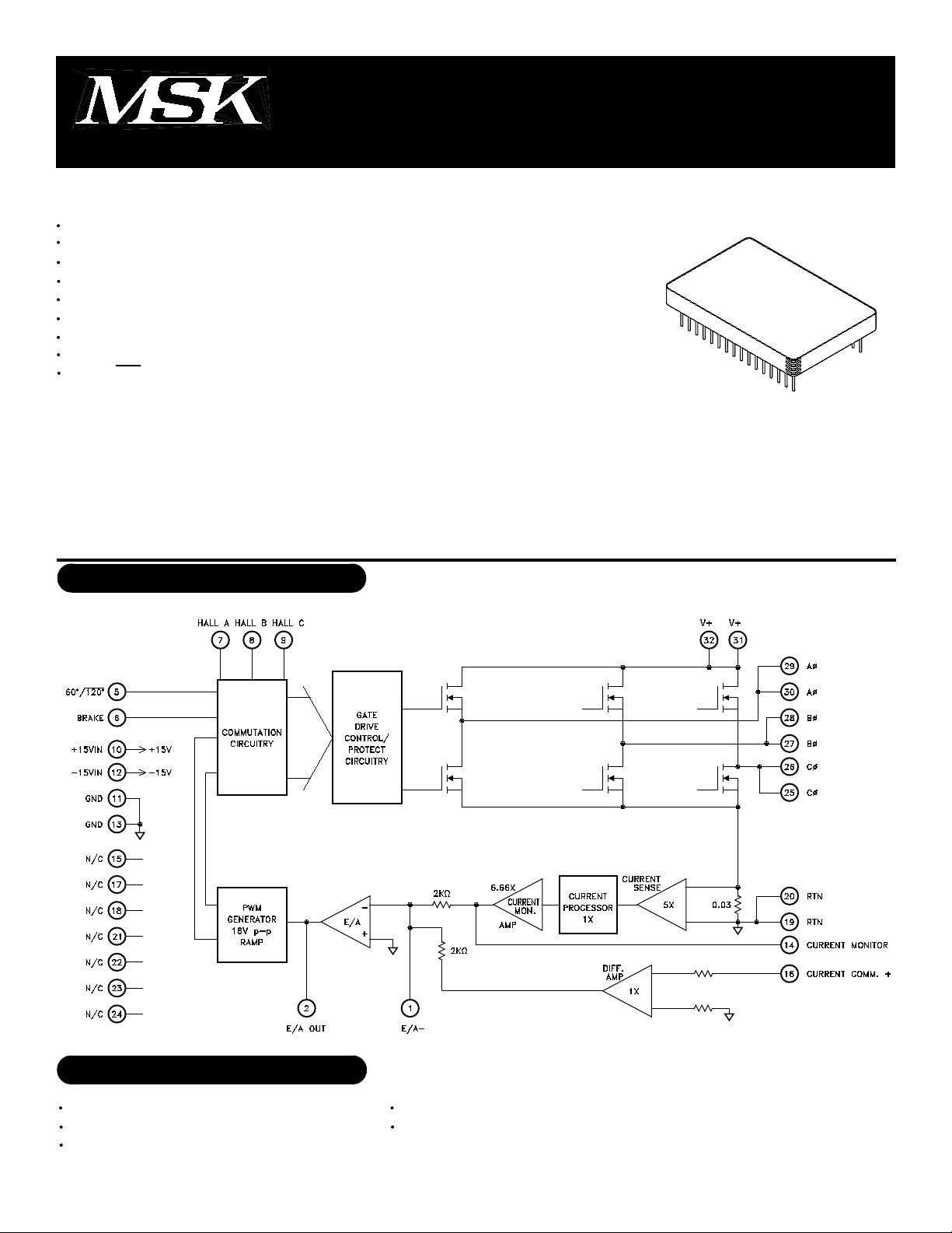
The MSK 4364 is a complete 3 Phase MOSFET Bridge Brushless Motor Control System in an electrically isolated
hermetic package. The hybrid is capable of 5 amps of output current and 55 volts of DC bus voltage. It has the
normal features for protecting the bridge. Included is all the bridge drive circuitry, hall sensing circuitry, commutation
circuitry and all the current sensing and analog circuitry necessary for closed loop current mode (torque) control.
When PWM'ing, the transistors are modulated in locked anti-phase mode for the tightest control and the most
bandwidth. Provisions for applying different compensation schemes are included. The MSK 4364 has good thermal
conductivity of the MOSFET's due to isolated substrate/package design that allows direct heat sinking of the hybrid
without insulators.
4364
EQUIVALENT SCHEMATIC
TYPICAL APPLICATIONS
3 Phase Brushless DC Motor Control
Servo Control
Fin Actuator Control
Gimbal Control
AZ-EL Control
1 Rev. A 1/02
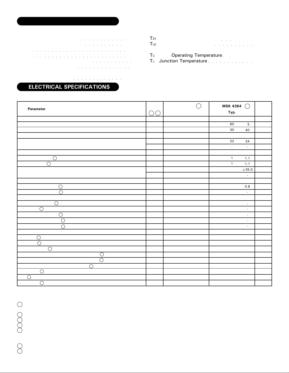
ABSOLUTE MAXIMUM RATINGS
V+
VIN
+Vcc
-Vcc
IOUT
IPK
θJC
High Voltage Supply
Current Command Input
○○○○○○○○○○○○○○○○○○○○○○○○○
○○○○○○○○○○○○○○○○○○○○○○○○○
Continuous Output Current
Peak Output Current
○○○○○○○○○○○○○○
○○○○○○○○○○
○○○○○○○○○○○
○○○○○○○○○○○○○○
Thermal Resistance @ 25°C
(Junction To Case)
○○○○○○○○○○○○○
ELECTRICAL SPECIFICATIONS
Parameter
POWER SUPPLY REQUIREMENTS
+Vcc
-Vcc
PWM
Free Running Frequency
CONTROL
Transconductance
Current Monitor
Output Offset
HALL INPUTS
Low Level Input Voltage
High Level Input Voltage
ERROR AMP
Input Voltage Range
Slew Rate
Output Voltage Swing
Gain Bandwidth Product
Large Signal Voltage Gain
OUTPUT
Rise Time
Fall Time
Leakage Current
Voltage Drop Across Bridge (1 Upper and 1 Lower)
Voltage Drop Across Bridge (1 Upper and 1 Lower)
Drain-Source On Resistance (Each MOSFET)
Diode VSD
trr
Dead Time
1
1
1
7
7
1
1
1
1
1
1
1
1
6
1
1
55V
±13.5V
+16V
-18V
5A
10A
11°C/W
Test Conditions
@ +15V
@ -15V
±5 Amps Output
±5 Amps Output
@ 0 Volts Command
@ 44V, +150°C Junction
1
@ 5 Amps
1
@ 5 Amps, +150°C Junction
@ 5 Amps, 150°C Junction
@ 5 Amps, Each FET
IF=5 Amps, di/dt=100A/µS
TST
Storage Temperature Range
TLD
Lead Temperature Range
(10 Seconds)
TC
Case Operating Temperature
TJ
Junction Temperature
All Ratings: Tc=+25°C Unless Otherwise Specified
Group A
Subgroup
4
1,2,3
1,2,3
4
5,6
4,5,6
4,5,6
4
5,6
-
-
-
-
-
-
-
-
-
-
-
-
-
-
-
-
5
MSK 4364H/E
Min.
18.7
0.95
±11
±12
21
0.9
3.0
6.5
175
Typ.
-
60
-
30
22
-
1
1
-
±5.0
-
-
-
-
-
-
-
-
-
-
-
-
-
-
-
±12
8
±13
6.5
275
100
100
-
-
-
-
-
280
2
○○○
○○○○○○○○○○
○○
○○○○○○○○○○○○
3
Max.
85
40
23
25.3
1.05
1.1
±25.0
±50.0
0.8
-
-
-
-
-
-
-
-
750
0.6
1.2
.100
1.6
-
-
MSK 4364
Min.
-
-
20
-
0.9
0.9
-
-
-
3.0
±11
6.5
±12
-
175
-
-
-
-
-
-
-
-
-
-65°C to +150°C
+300°C
-55°C to +125°C
+150°C
2
85
40
24
1.1
1.1
0.8
0.6
1.2
1.6
-
-
-
-
-
-
-
-
-
-
-
-
Units
mA
mA
KHz
KHz
Amp/Volt
V/Amp
mAmp
mAmp
Volts
Volts
Volts
V/µSec
Volts
MHz
V/mV
nSec
nSec
µAmps
Volts
Volts
Ω
Volts
nSec
µSec
Typ.
60
30
22
-
1
1
±5.0
-
-
-
±12
8
±13
6.5
275
100
100
-
-
-
-
-
280
2
Max.
±35.0
750
.100
NOTES:
1 Guaranteed by design but not tested. Typical parameters are representative of actual device
performance but are for reference only.
2 Industrial grade and 'E' suffix devices shall be tested to subgroups 1 and 4 unless otherwise specified.
3 Military grade devices ("H" Suffix) shall be 100% tested to Subgroups 1, 2, 3 and 4.
4 Subgroups 5 and 6 testing available upon request.
5 Subgroup 1, 4 TA = TC = +25°C
2, 5 T
3, 6 T
A = TC = +125°C
A = TC = -55°C
6 This is to be used for MOSFET thermal calculation only.
7 Measurements do not include offset current at 0V current command.
2
Rev. A 1/02

APPLICATION NOTES
MSK 4364 PIN DESCRIPTIONS
V+ - are the power connections from the hybrid to the bus.
All three pins for the motor voltage supply should be con-
nected together to share the current through the three pins in
the hybrid. The external wiring to these pins should be sized
according to the RMS current required by the motor. A high
quality monolithic ceramic capacitor for high frequencies and
enough bulk capacitance for keeping the V+ supply from
drooping should bypass these pins. 470µF is recommended.
Capacitors should be placed as close to these pins as practi-
cal.
AØ, BØ & CØ- are the connections to the motor phase wind-
ings from the bridge output. The wiring to these pins should
be sized according to the required current by the motor. There
are no short circuit provisions for these outputs. Shorts to
V+ or gound from these pins must be avoided or the bridge
will be destroyed. All three pins for each phase should be
connected together to share the current through the three
pins in the hybrid.
RTN - is the power return connection from the module to the
bus. All internal ground returns connect to this point inside
the hybrid. All three pins should be connected together to
share the current. All capacitors from the V+ bus should
connect to this point as close as possible. All external V+
return connections should be made as close to these pins as
possible. Wiring sizing to this pin should be made according
to the required current.
GND - is the return point for the low powered circuitry inside
the hybrid. All GND pins should be tied together. All capaci-
tors for bypassing the + and -15V supplies should be tied at
this point, as close to the pins as possible. Any ground plane
connections for low powered and analog citcuitry outside the
hybrid should be tied to this point.
+15VIN - is the input for applying +15 volts to run the low
power section of the hybrid. Both pins should be used to-
gether for optimum operation. These pins should be bypassed
with a 10µF capacitor and a 0.1µF capacitor as close to these
pins as possible.
HALL A,B,C - are the hall input pins from the hall devices in
the motor. These pins are internally pulled up to 6.25 volts.
The halls can reflect a 120/240 degree commutation or a 60/
300 degree scheme.
BRAKE - is a pin for commanding the output bridge into a
motor BRAKE mode. When pulled low, normal operation pro-
ceeds. When pulled high, the three high side bridge transis-
tors turn off and the three low side transistors turn fully on
without PWM'ing. This will cause rapid deceleration of the
motor and will cease motor operation until pulled high again.
Logic levels for this input are TTL compatible. It is internally
pulled high.
60/120 - is a pin for selecting the orientation scheme of the
motor. A high state will produce 60/300 degree commuta-
tion, whereas a low state will produce 120/240 degree com-
mutation. Logic levels for this input are TTL compatible. It is
internally pulled high.
CURRENT COMMAND (+) - is the input for controlling the
module in current mode. Scaled at 1 amp per volt of input
command, the bipolar input allows both forward and reverse
current control capability regardless of motor commutation
direction. The maximum operational command voltage should
be ±5 volts for ±5 amps of motor current. Going beyond 5
volts of command voltage will force the bridge to conduct
more than the desired maximum current. There is internal
current limiting that will ultimately limit the absolute maxi-
mum current being output by the bridge.
CURRENT MONITOR- is a pin providing a current viewing
signal for external monitoring purposes. This is scaled at ±1
amp of motor current per volt output, up to a maximum of
±5 volts, or ±5 amps. Going beyond the 5 volt maximum
may result in clipping of the waveform peaks.
E/A OUT - is the current loop error amplifier output. It is
brought out for allowing various loop compensation circuits
to be connected between this and E/A-.
IN
-15VIN - is the input for applying -15 volts to run the low
power section of the hybrid. Both pins should be used to-
gether for optimum operation. These pins should be bypassed
with a 10µF capacitor and a 0.1µF capacitor as close to these
pins as possible.
E/A- - is the current loop error amplifier inverting input. It is
brought out for allowing various loop compensation circuits
to be connected between this and E/A OUT.
3 Rev. A 1/02
 Loading...