

MSK MSK4362D, MSK4362HU, MSK4362U, MSK4362S Datasheet
ISO 9001 CERTIFIED BY DSCC
30 AMP, 75V, 3 PHASE
MOSFET BRUSHLESS
M.S.KENNEDY CORP.
4707 Dey Road Liverpool, N.Y. 13088 (315) 701-6751
FEATURES:
75 Volt Motor Supply Voltage
30 Amp Output Switch Capability
100% Duty Cycle High Side Conduction Capable
Shoot-Through/Cross Conduction Protection
Hall Sensing and Commutation Circuitry on Board
"Real" Four Quadrant Torque Control Capability
Good Accuracy Around the Null Torque Point
Isolated Package Design for High Voltage Isolation Plus Good Thermal Transfer
60°/ 120º Phasing Selectable
Plus and Minus 15 Volt Regulated Voltage Outputs are available for Powering Other Circuitry.
MOTOR CONTROLLER
MIL-PRF-38534 QUALIFIED
DESCRIPTION:
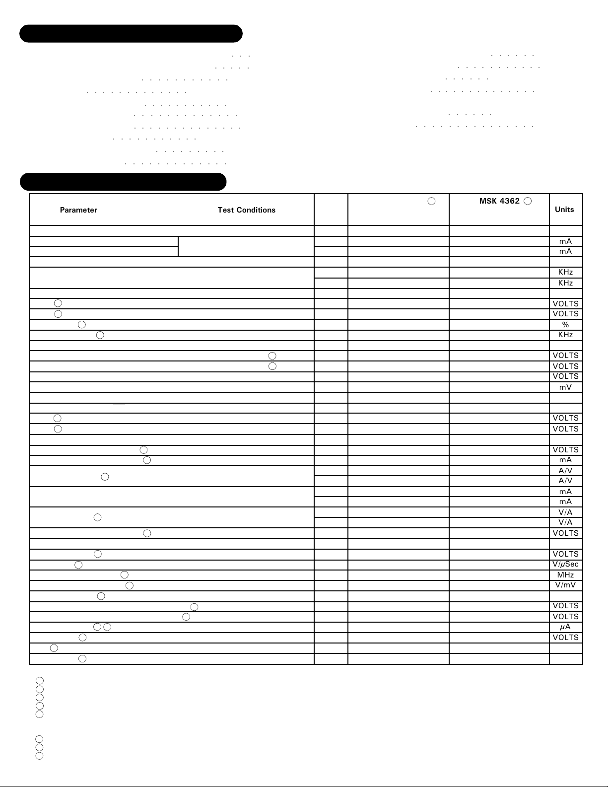
The MSK 4362 is a complete 3 Phase MOSFET Bridge Brushless Motor Control System in a convenient isolated
hermetic package. The hybrid is capable of 30 amps of output current and 75 volts of DC bus voltage. It has the
normal features for protecting the bridge. Included is all the bridge drive circuitry, hall sensing circuitry, commutation
circuitry and all the current sensing and analog circuitry necessary for closed loop current mode (torque) control.
When PWM'ing, the transistors are modulated in locked anti-phase mode for the tightest control and the most
bandwidth. Provisions for applying different compensation schemes are included. The MSK 4362 has good thermal
conductivity of the MOSFET's due to isolated package design that allows direct heat sinking of the hybrid without
insulators.
4362
BLOCK DIAGRAM
TYPICAL APPLICATIONS
3 Phase Brushless DC Motor Control
Servo Control
Fin Actuator Control
Gimbal Control
AZ-EL Control
PIN-OUT INFORMATION
1 REFOUT 13 E/A - 25+REG IN 37 BØ
2 HALL A 14 GND 26 LGND 38 BV+
3 HALL B 15 +Current Command 27 RTN 39 AVS
4 HALL C 16 -Current Command 28 RTN 40 AVS
5 60 /120 17 +15 VIN 29 CVS 41 AØ
6 BRAKE 18 Current Monitor Out 30 CVS 42 AØ
7 CLOCK SYNC 19 -15 VIN 31 CØ 43 AV+
8 DIS 20 -REG IN 32 CØ
9 GND 21 L1 33 CV+
10 N/C 22 -15 VOUT 34 BVS
11 N/C 23 GND 35 BVS
12 E/A OUT 24 +15 VOUT 36 BØ
1
Rev. F 6/00
ABSOLUTE MAXIMUM RATINGS
High Voltage Supply (internal regulators disabled)
High Voltage Supply (using internal regulators)
Current Command Input
Logic Inputs
○○○○○○○○○○○○○
±15VOUT External Load
REFOUT External Load
E/A OUT External Load
Clock SYNC Input
Continuous Output Current
Peak Output Current
○○○○○○○○○○○
○○○○○○○○○○○
○○○○○○○○○○○○○
○○○○○○○○○○○○○○
○○○○○○○○○○○
○○○○○○○○○
○○○○○○○○○○○○○
○○○○○
-0.2V to REFOUT
-0.2V to +15V
ELECTRICAL SPECIFICATIONS
75V
○○○
55V
±13.5V
±25 mA
15 mA
5 mA
30 Amps
41 Amps
Thermal Resistance (Output Switches)
RθJC
Thermal Resistance (Regulator)
RθJC
Storage Temperature Range
TST
Lead Temperature Range
TLD
○○○○○○○○○○○○○○
(10 Seconds)
Case Operating Temperature
TC
Junction Temperature
TJ
○○○○○○○○○○○○○○○
○○○○○○
○○○○○○○○○○○
○○○○○○
○○○○○○
-65°C to +150°C
-55°C to +125°C
1.5°C/W
9°C/W
+300°C
+150°C
Parameter
INPUT CURRENT
+15 VIN
-15 VIN
PWM
Clock Free Running Frequency
CLOCK SYNC INPUT
1
VIL
1
VIH
Duty Cycle
SYNC Frequency
REGULATORS
+15 VOUT
-15 VOUT
REFOUT
-15 VOUT Ripple
LOGIC INPUTS
(Hall A,B,C,Brake,60°/120°,DIS)
VIL
VIH
ANALOG SECTION
Current Command Input Range
Current Command Input Current
Transconductance
Offset Current
Current Monitor
Current Monitor Voltage Swing
ERROR AMP
E/A OUT Swing
Slew Rate
Gain Bandwidth Product
Large Signal Voltage Gain
OUTPUT SECTION
Voltage Drop Across Bridge (1 Upper & 1 Lower)
Voltage Drop Across Bridge (1 Upper & 1 Lower)
Leakage Current
Diode VSD
trr
Dead Time
1
1
1
1
1
1
8
8
1
1
1
1
1
1
1
1
1
1
7
Test Conditions
Output PWM'ing
Current Command=0 Volts
25mA Load
25mA Load
15mA Load
50mA Load
6
6
Group A
Subgroup
Current Command=0Volts
5mA Load
5mA Load
1
1
30 AMPS @ 150°c Junction
All switches off, V+=60V, 150°C Junction
30 AMPS
1
1
4
5,6
-
-
-
-
1,2,3
1,2,3
1,2,3
4
-
-
-
-
4
5,6
1
2,3
4
5,6
-
-
-
-
-
-
-
-
-
-
MSK 4362(H)
Min. Typ. Max.
-
68
-
30
21
18.7
12.5
10
Clock +0
14.25
-14.25
5.82
3.0
-13.5
2.70
2.55
-25
-50
0.300
0.280
-12
-12
6.5
175
22
22
-
-
-
-
-
Clock +3
-
-
-
-
-
-
-
-
-
-
-
3
3
0
0
0.33
0.33
-
-
8
-
6.5
275
-
-
-
-
-
-
-
-
-
-
280
2
25.3
15.75
-15.75
6.57
250
+13.5
3.30
3.45
0.367
0.380
+12
+12
1.83
750
NOTES:
1
Guaranteed by design but not tested. Typical parameters are representative of actual device performance but are for reference only.
2
Industrial grade devices shall be tested to subgroups 1 and 4 unless otherwise specified.
3
Military grade devices ("H" Suffix) shall be 100% tested to Subgroups 1, 2, 3 and 4.
4
Subgroups 5 and 6 testing available upon request.
5
Subgroup 1, 4 TA = TC = +25°C
6
Maximum power dissipation must be limited according to voltage regulator power dissipation.
7
Hybrid powered by external ±15V supplies.
8
Measurements do not include offset current at 0V current command.
2, 5 TA =TC =+125°C
3, 6 TA =TC = -55°C
2
85
40
23
2.5
90
0.8
1.5
25
50
1
2.6
3
Min. Typ. Max.
-
-
20
-
-
12.5
-
10
Clock +0
14.25
-14.25
5.82
-
-
-
3.0
-13.5
-
2.55
-
-50
-
0.280
-
-12
-12
-
-
-
6.5
-
175
-
-
-
-
-
-
-
-
MSK 4362
68
30
22
-
-
-
-
-
-
-
-
-
-
-
-
-
3
-
0
-
0.33
-
-
-
8
6.5
275
-
-
-
-
280
2
2
Units
85
40
24
2.5
mA
mA
KHz
KHz
-
VOLTS
VOLTS
-
90
Clock +3
15.75
-15.75
6.57
250
0.8
+13.5
1.5
3.45
50
0.380
+12
+12
1.83
KHz
VOLTS
VOLTS
VOLTS
mV
VOLTS
VOLTS
-
VOLTS
mA
A/V
A/V
-
mA
mA
-
V/A
V/A
-
VOLTS
VOLTS
V/µSec
-
MHz
-
V/mV
-
VOLTS
1
VOLTS
750
VOLTS
2.6
nSec
-
µSec
-
Rev. F 6/00
%
µA

APPLICATION NOTES
MSK 4362 PIN DESCRIPTIONS
AV+, BV+, CV+ - are the power connections from the hy-
brid to the bus. The pins for each phase are brought out
separately and must be connected together to the V+ source
externally. The external wiring to these pins should be sized
according to the RMS current required by the motor. These
pins should be bypassed by a high quality monolithic ceramic
capacitor for high frequencies and enough bulk capacitance
for keeping the V+ supply from drooping. 78 µF of ceramic
capacitance and 6200 µF of bulk capacitance was used in
the test circuit. The voltage range on these pins is from 16
volts up to 75 volts.
AØ, BØ & CØ- are the connections to the motor phase wind-
ings from the bridge output. The wiring to these pins should
be sized according to the required current by the motor. There
are no short circuit provisions for these outputs. Shorts to
V+ or gound from these pins must be avoided or the bridge
will be destroyed.
AVS, BVS, CVS - are the return pins on the bottom of each
half bridge. They are brought out separately and should be
connected together externally to allow the current from each
half bridge to flow through the sense resistor. The wiring on
these pins should be sized according to the current require-
ments of the motor.
-REF IN - is the input pin for applying power to the internal
-15V DC - DC converter. To use the converter, connect the
-REG IN pin to +15 VOUT pin. If the -15V converter is not
needed, no connection should be made to -REG IN and -15
VOUT. -15 volts will have to be supplied from an external
source to -15VIN. Also, L1 can be left open. See voltage
regulator portion of app. note for additional information.
L1 - is a pin for connecting an external inductor to the DC -
DC converter for generating -15 volts. A 47 µH inductor
capable of running at 250 KHz and about 1 amp of DC cur-
rent shall be used. Connect the inductor between L1 and
GND.
-15 VOUT - is a regulated -15 volt output available for exter-
nal uses. Up to 25 mA is available at this pin. A 100 micro-
farad capacitor should be connected as close to this pin as
possible and returned to GND along with a 0.22 microfarad
monolithic ceramic capacitor. CAUTION: See Voltage Regu-
lator Power Dissipation
-15 VIN - is the input for applying -15 volts to run the low
power section of the hybrid. This pin should be connected to
-15 VOUT if running off of the internal regulator. The re-
quired bypassing of the -15 VOUT pin is sufficient in this
case. For bringing in -15 volts, this pin should be bypassed
with a 10 µF capacitor and a 0.1 µF capacitor as close to this
pin as possible.
RTN - is the power return connection from the module to the
bus. All ground returns connect to this point from internal to
the module in a star fashion. All external ground connections
to this point should also be made in a similar fashion. The
V+ capacitors should be returned to this pin as close as
possible. Wire sizing to this pin connection should be made
according to the required current.
LGND - is an isolated ground connection to the RTN pin of
the hybrid that is connected internally. For any circuitry that
needs to be connected to the RTN pin without the influence
of current flow through RTN should be connected at this
point.
GND - is a ground pin that connects to the ground plane for
all low powered circuitry inside the hybrid.
+REG IN - is the input pin for applying power to the internal
+15V regulator. To use the regulator, connect the +REG IN
pin to the motor bus (V+). See regulator app. note for more
info on input voltage. If the +15V regulator is not needed,
no connection should be made to +REG IN and +15 VOUT.
+15 volts will have to be supplied from an external source to
+15VIN. Absolute maximum voltage on this pin is 55 volts.
See voltage regulator portion of app. note for additional infor-
mation.
+15 VOUT- is a regulated +15 volt output available for ex-
ternal uses. Up to 25 mA is available at this pin. A 100
microfarad capacitor should be connected as close to this pin
as possible and returned to GND along with a 0.22 micro-
farad monolithic ceramic capacitor. CAUTION: See Voltage
Regulator Power Dissipation.
+15 VIN - is the input for applying +15 volts to run the low
power section of the hybrid. This pin should be connected to
+15 VOUT if running off of the internal regulator. The re-
quired bypassing of the +15 VOUT pin is sufficient in this
case. For bringing in external +15 volts, this pin should be
bypassed with a 10 µF capacitor and a 0.1 µF capacitor as
close to this pin as possible.
CURRENT COMMAND (+,-) - are differential inputs for con-
trolling the module in current mode. Scaled at ±3 amps per
volt of input command, the bipolar input allows both forward
and reverse current control capability regardless of motor com-
mutation direction. The maximum operational command volt-
age should be ±10 volts for ±30 amps of motor current.
CURRENT MONITOR- is a pin providing a current viewing sig-
nal for external monitoring purposes. This is scaled at ±3
amps of motor current per volt output, up to a maximum of
±10 volts, or ±30 amps. As ±30 amps is exceeded, the
peaks of the waveform may become clipped as the rails of
the amplifiers are reached. This voltage is typically ±12.5
volts, equating to ±37 amps of current peaks.
E/A OUT - is the current loop error amp output connection.
It is brought out for allowing various loop compensation cir-
cuits to be connected between this and E/A-.
E/A- -is the current loop error amp inverting input connec-
tion. It is brought out for allowing various loop compensa-
tion circuits to be connected between this and E/A OUT.
CLOCK SYNC- is an input for synchronizing to an external
clock. The sync circuit will trigger on the edges of the ap-
plied clock and effectively shorten the period of the internal
oscillator on each cycle. The frequency can be increased
from a free running 22 KHz to 25 KHz maximum. The clock
applied shall be 15 volts amplitude with at least a 10% duty
cycle.
REFOUT- is a 6.25 volt regulated output to be used for pow-
ering the hall devices in various motors. Up to 15 mA of
output current is available.
HALL A, B & C - are the hall input pins from the hall devices
in the motor. These pins are internally pulled up to 6.25
volts. The halls can reflect a 120/240 degree commutation
scheme or a 60/300 degree scheme.
3
IN
Rev. F 6/00
 Loading...