

MSK MSK4223U, MSK4223D, MSK4223S Datasheet
ISO 9001 CERTIFIED BY DSCC
75 VOLT 6 AMP MOSFET
H-BRIDGE PWM MOTOR
4223
M.S.KENNEDY CORP.
4707 Dey Road Liverpool, N.Y. 13088 (315) 701-6751
FEATURES:
Low Cost Complete H-Bridge
6 Amp Capability, 75 Volt Maximum Rating
Self-contained Smart Lowside/Highside Drive Circuitry
Internal PWM Generation, Shoot-through Protection
Isolated Case Allows Direct Heatsinking
Four Quadrant Operation, Torque Control Capability
Logic Level Disable Input
Logic Level High Side Enable Input for Special Modulation or Function
Available With Leads Bent Up Or Down
DESCRIPTION:
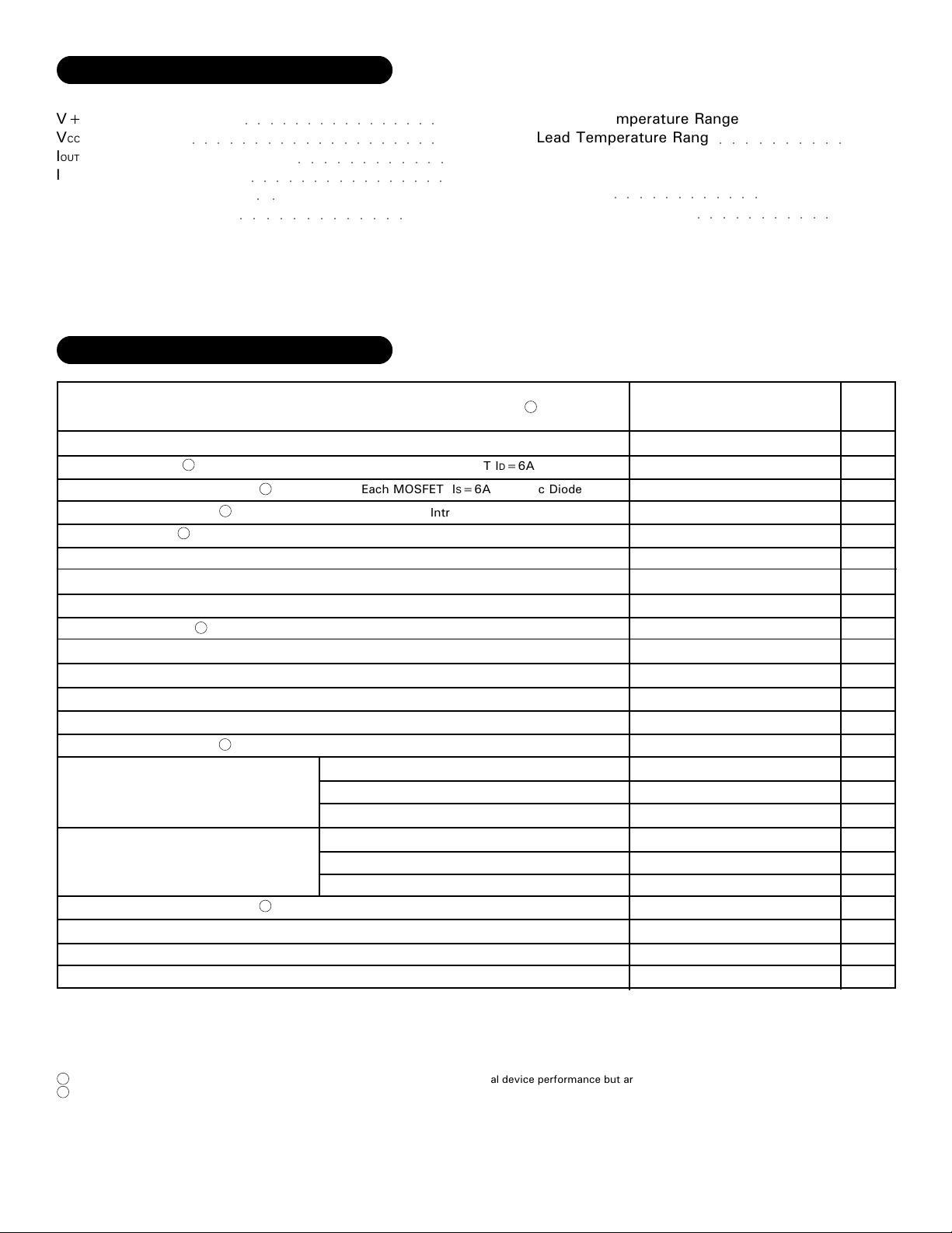
The MSK 4223 is a complete H-Bridge circuit to be used for DC brushed motor control or Class D switchmode
amplification. All of the drive/control circuitry for the lowside and highside switches are internal to the circuit. The
PWM circuitry is internal as well, leaving the user to only provide an analog signal for the motor speed/direction, or
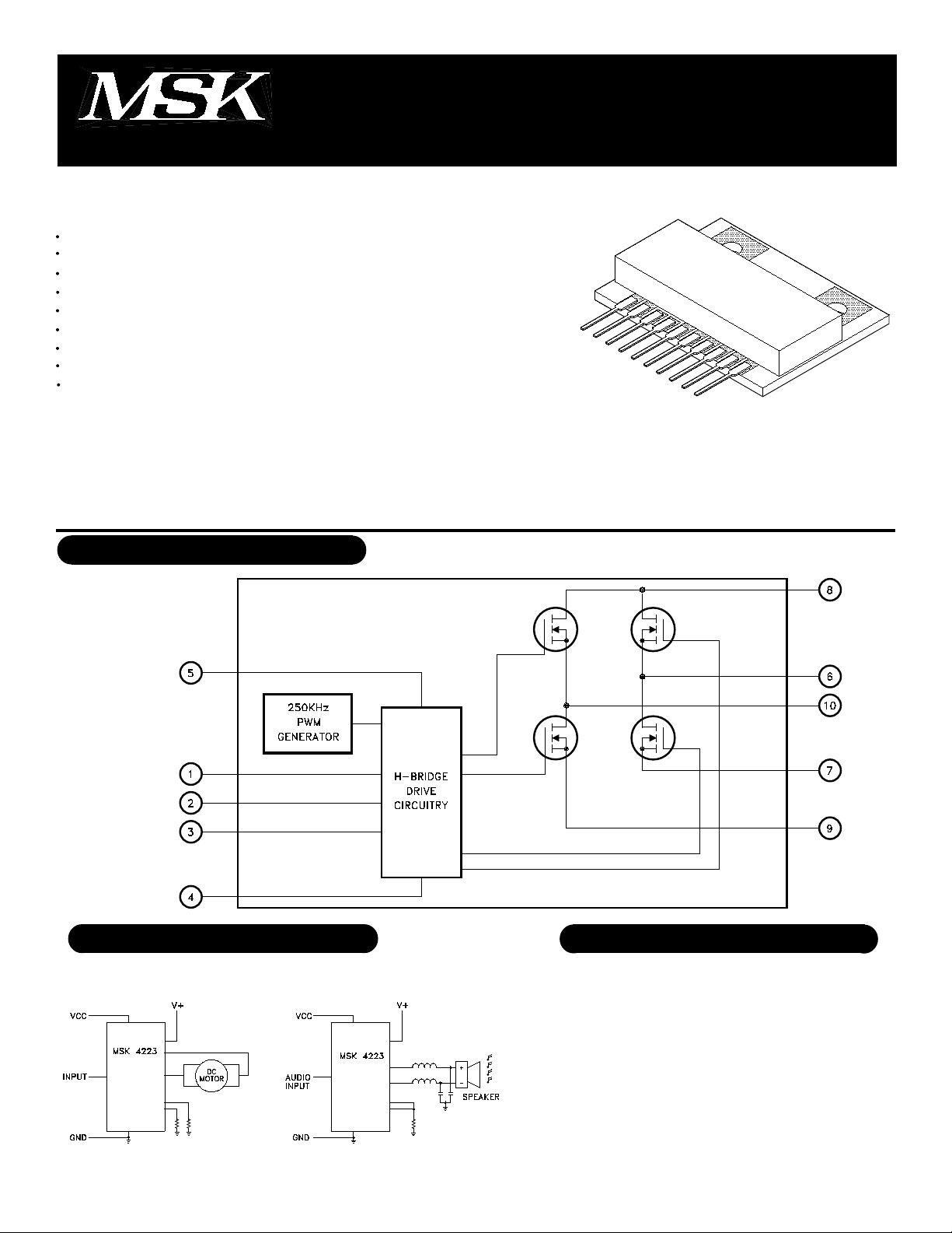
audio signal for switchmode audio amplification. The MSK 4223 is constructed on a space efficient ceramic sub-
strate that can be directly connected to a heatsink.
DRIVER/AMPLIFIER
EQUIVALENT SCHEMATIC
TYPICAL APPLICATIONS
PIN-OUT INFORMATION
HEN
1
Disable
2
Input
3
Ground
4
Vcc
5
Output A
6
Rsense A
7
V+
8
Rsense B
9
Output B
10
1
PRELIMINARY Rev. F 10/00
ABSOLUTE MAXIMUM RATINGS
High Voltage Supply
V+
Logic Supply
VCC
Continuous Output Current
IOUT
Peak Output Current
IPK
Output Voltage Range
VOUT
Thermal Resistance
θJC
○○○○○○○○○○○○○○○○○○○○
○○○○○○○○○○○○○○○○
○○○○○○○○○○○○
○○○○○○○○○○○○○○○○
○○
GND-2V min. To V+ max.
○○○○○○○○○○○○○
(Output Switches)
ELECTRICAL SPECIFICATIONS
75V
16V
6A
9A
4.6°C/W
Storage Temperature Range
TST
Lead Temperature Range
TLD
-65°C to +150°C
○○○○○○○○○○
(10 Seconds)
Case Operating Temperature
TC
MSK4223
Junction Temperature
TJ
○○○○○○○○○○○○
○○○○○○○○○○○
-40°C to +125°C
+150°C
All Ratings: Tc= +25°C Unless Otherwise Specified
300°C
Parameter
OUTPUT CHARACTERISTICS
VDS(ON) Voltage
Instantaneous Forward Voltage
Reverse Recovery Time
Leakage Current
PWM Frequency
Vcc SUPPLY CHARACTERISTICS
Quiescent Bias Current
Vcc Voltage Range
INPUT SIGNAL CHARACTERISTICS
Analog Input Voltage
Analog Input Voltage
Analog Input Voltage
LOGIC CONTROL INPUTS
Disable Input
HEN Input
SWITCHING CHARACTERISTICS
Rise-Time
Fall-Time
Dead-Time
1
1
1
1
1
-
-
-
-
-
9
-
-
-
-
-
-
-
MSK 4223
Typ.
0.75
1.1
-
1.0
250
46
12
6
3
9
-
-
-
-
-
-
56
33
100
Max.
1.5
1.8
260
25
275
60
16
6.5
3.5
9.5
0.8
-
-135
0.8
-
-270
84
50
-
Units
V
V
nS
uA
KHz
mA
V
V
V
V
V
V
uA
V
V
uA
nS
nS
nS
Test Conditions
Each MOSFET ID=6A
1
1
Each MOSFET IS=6A Intrinsic Diode
Intrinsic Diode
Each MOSFET V+=70V
Analog Input=6VDC RL=∞
Output A,B=50% Duty Cycle
Output A=100% Duty Cycle High
Output B=100% Duty Cycle High
Input Voltage LO
Input Voltage HI
Input Current (DISABLE=0V)
Input Voltage LO
Input Voltage HI
Input Current (HEN=0V)
RL=100Ω
V+=75V
V+=75V
2
Min.
225
5.5
2.5
8.5
2.7
2.7
NOTES:
1
Guaranteed by design but not tested. Typical parameters are representative of actual device performance but are for reference only.
2
Vcc=+12V, V+=28V, RL=1K AOUT to BOUT, unless otherwise specified.
2
PRELIMINARY Rev. F 10/00
 Loading...