

MSK MSK4201, MSK4201B Datasheet
ISO 9001 CERTIFIED BY DESC
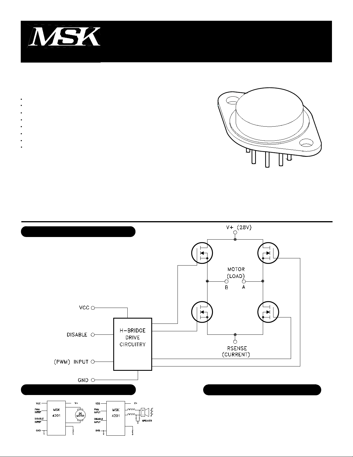
28 VOLT 5 AMP MOSFET
H-BRIDGE PWM MOTOR
4201
M.S.KENNEDY CORP.
4707 Dey Road Liverpool, N.Y. 13088 (315) 701-6751
FEATURES:
Low Cost Complete H-Bridge
28 Volt, 5 Amp Capability, 75 Volt Maximum Rating
Self-contained Smart Lowside/Highside Drive Circuitry
Internal Deadtime Generation, Shoot-through Protection
Output Disable/Shutdown Capability
Isolated Case Allows Direct Heatsinking
Four Quadrant Operation, Torque Control Capability
Available Fully Screened To MIL-H-38534
DESCRIPTION:
The MSK 4201 is a complete H-Bridge hybrid to be used for DC brushed motor control or Class D switchmode
amplifier. All of the drive/control circtuitry for the lowside and highside switches are internal to the hybrid. The user
provides a TTL compatible PWM signal for simultaneous amplitude and direction control in four quadrant mode. The
internal drive circuitry will provide proper deadtime/shoot-through protection for each half-bridge. All N-channel FETs
mean the best efficiency for the size, both in terms of on-resistance and switching capability. For an idle/sleep mode,
or for fault protection, a TTL compatible disable pin is provided so as to shut down all four transistors. The MSK 4201
is packaged in a space efficient isolated 8 pin TO-3 that can be directly connected to a heatsink.
DRIVER/AMPLIFIER
MIL-PRF-38534 CERTIFIED
EQUIVALENT SCHEMATIC
TYPICAL APPLICATIONS
PIN-OUT INFORMATION
5
V+
1
MOTOR B
2
VCC
3
DISABLE
4
1
GND
6
INPUT
7
MOTOR A
8
RSENSE
Rev. B 6/00
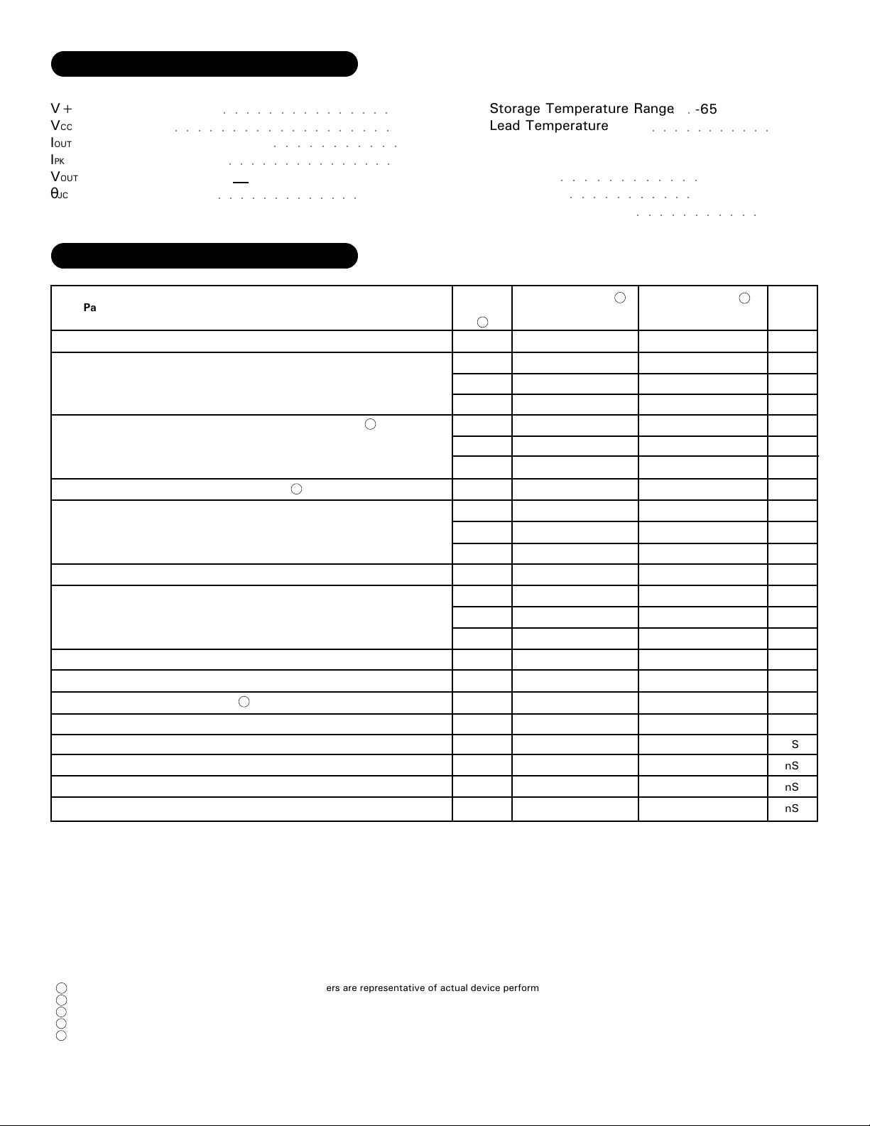
ABSOLUTE MAXIMUM RATINGS
High Voltage Supply
V+
Logic Supply
VCC
Continuous Output Current
IOUT
Peak Output Current
IPK
Output Voltage Range
VOUT
Thermal Resistance
θJC
○○○○○○○○○○○○○○○○○○○
○○○○○○○○○○○○○○○
○○○○○○○○○○○
○○○○○○○○○○○○○○○
GND-2V min. To V+ max.
○○○○○○○○○○○○○
(Output Switches)
ELECTRICAL SPECIFICATIONS
Parameter
OUTPUT CHARACTERISTICS
VDS(ON) Voltage (Each MOSFET)
Instantaneous Forward Voltage, Each MOSFET
(Intrinsic Diode)
Reverse Recovery Time (Intrinsic Diode)
Leakage Current, Each MOSFET
LOGIC SUPPLY CHARACTERISTICS
Quiescent Logic Current
INPUT SIGNALS CHARACTERISTICS
Threshold Voltage
SWITCHING CHARACTERISTICS
Turn-On Propagation Delay (Includes Deadtime)
Turn-Off Propagation Delay
Rise-Time
Fall-Time
Dead-Time
Test Conditions
1
V+=28V, VCC=12V, IC=2A
1
2.6°C/W
ID=2A
1
IS=2A
V+=75V
V+=70V
V+=75V
VCC=12V
(non-switching)
VCC=12V
75V
16V
5A
37A
Storage Temperature Range
TST
Lead Temperature Range
TLD
○○
-65°C to +150°C
○○○○○○○○○○○
(10 Seconds)
Case Operating Temperature
TC
MSK4201
MSK4201B
Junction Temperature
TJ
○○○○○○○○○○○○
○○○○○○○○○○○
○○○○○○○○○○○
-55°C to +125°C
-25°C to +85°C
+175°C
All Ratings: Tc= +25°C Unless Otherwise Specified
Subgroup
Group A
5
1
2
3
1
2
3
-
1
2
3
1
2
3
1,2,3
4
4
4
44
4
44
4
-
MSK 4201B
Min.
-
-
-
-
-
-
-
-
-
-
-
-
-
0.8
-
-
-
-
-
Typ.
0.55
0.90
0.36
0.95
0.85
1.0
-
1.0
2.0
0.5
11
11
11
1.5
160
85
36
170
100
3
Max.
0.8
1.2
0.60
1.1
0.95
1.25
240
5
10
5
15
15
15
2.7
TBD
TBD
TBD
TBD
-
Min.
-
-
-
-
-
-
-
-
-
-
-
-
-
0.8
-
-
-
-
-
MSK 4201
Typ.
0.55
-
-
0.95
-
-
-
1.0
-
-
11
-
-
1.5
160
85
36
170
100
2
Max.
1.0
-
-
1.2
-
-
240
10
-
-
15
-
-
2.7
-
-
-
-
-
300°C
Units
V
V
V
V
V
V
nS
uA
uA
uA
mA
mA
mA
V
nS
nS
nS
nS
nS
NOTES:
Guaranteed by design but not tested. Typical parameters are representative of actual device performance but are for reference only.
1
Industrial grade devices shall be tested to subgroups 1 and 4 unless otherwise specified.
2
Military grade devices ("B" suffix) shall be 100% tested to subgroups 1,2,3 and 4.
3
Subgroups 5 and 6 testing available upon request.
4
Subgroup 1,4 T
5
2 TA=TC= +125°C
3 TA=TC= -55°C
A=TC= +25°C
2
3030
30
3030
Rev. B 6/00

APPLICATION NOTES
MSK 4201 PIN DESCRIPTION
VCC - Is the low voltage supply for powering internal
logic and drivers for the lowside and highside MOSFETS.
The supplies for the highside drivers are derived from
this voltage.
V+ - Is the higher voltage H-bridge supply. The
MOSFETS obtain the drive current from this supply pin.
The voltage on this pin is limited by the drive IC. The
MOSFETS are rated at 100 volts. Proper by-passing to
GND with sufficient capacitance to suppress any volt-
age transients, and to ensure removing any drooping
during switching, should be done as close to the pins
on the hybrid as possible.
MOTOR A - Is the output pin for one half of the bridge.
When the PWM input is high, this output will be pulled
up to V+.
MOTOR B - Is the output pin for the other half of the
bridge. When the PWM input is low, this output will be
pulled up to V+.
RSENSE - This is the common connection for the bot-
tom of the bridge. This can have a sense resistor con-
nection to the V+ return ground for current limit sens-
ing, or can be connected directly to ground. The maxi-
mum voltage on this pin is ±2 volts with respect to
GND.
GND - Is the return connection for the input logic and
Vcc.
PWM INPUT - Is a TTL compatible input pin for provid-
ing the PWM signal to modulate the output switches.
The duty cycle can be between 0% (DC Low) and 100%
(DC High). See typical system operation notes.
DISABLE INPUT - Is a TTL compatible input for provid-
ing a shutdown signal to the hybrid for disabling all
four switches in the bridge regardless of the PWM in-
put level. A digital 1 disables, a digital 0 enables.
IN
3
Rev. B 6/00
 Loading...