

MSK MSK3554, MSK3554B Datasheet
ISO 9001 CERTIFIED BY DSCC
HIGH SPEED, WIDEBAND
OPERATIONAL AMPLIFIER
3554
M.S.KENNEDY CORP.
4707 Dey Road Liverpool, N.Y. 13088
FEATURES:
Stable at Low Gain
Fast Slew Rate - 1200V/µs Typical
Gain Bandwidth Product - 1200 MHz Typical
Low Quiescent Current - ±14.0 mA Typical
Low Offset - 2 mV Maximum
Drop In Replacement for OPA 3554 and TP 3554
High Output Current - ±100mA Minimum
MIL-PRF-38534 QUALIFIED
(315) 701-6751
DESCRIPTION:
The MSK 3554 is a pin compatible, low gain stable, drop-in replacement for the OPA 3554 and TP 3554. The
MSK 3554 does not exhibit high frequency output oscillations like other versions of the 3554 when operated at
closed loop gains of less than 55 V/V. The extremely low input bias current and input offset voltage ratings coupled
with a high slew rate and wide bandwidth make the MSK 3554 an excellent choice for fast D/A converters, buffers,
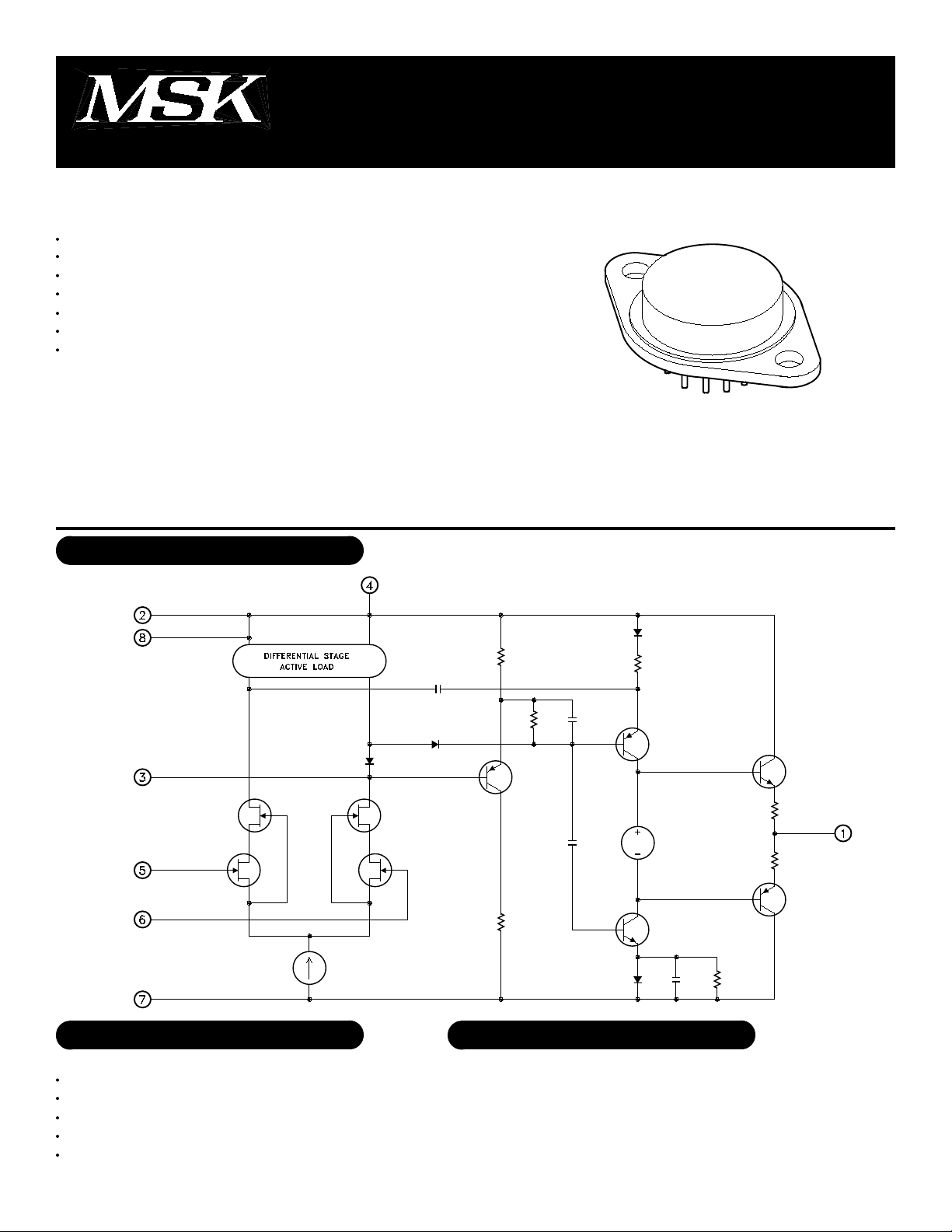
pulse amplifiers and other high speed op-amp applications. The MSK 3554 is packaged in an 8-pin TO-3 using thick
film hybrid technology to obtain high reliability and compact size.
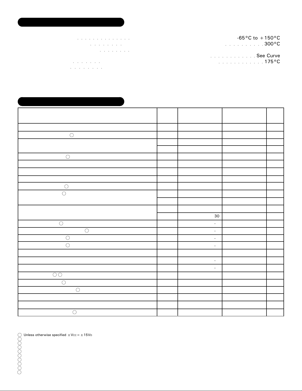
EQUIVALENT SCHEMATIC
TYPICAL APPLICATIONS
Fast D/A Converters
Pulse Amplifiers
Video Instrumentation
Fast Buffer/Follower
Video Frequency Filters
PIN-OUT INFORMATION
1
Output
2
Positive Power Supply
3
Compensation
4
Balance
8
Balance
7
Negative Power Supply
6
Non-Inverting Input
5
Inverting Input
Rev. B 7/001
ABSOLUTE MAXIMUM RATINGS
±VCC
IOUT
VIN
TC
Supply Voltage
○○○○○○○○○○○○○○
Peak Output Current
Differential Input Voltage
Case Operating Temperature
MSK 3554B
MSK 3554
○○○○○○○
○○○○○○○○
ELECTRICAL SPECIFICATIONS
Parameter
STATIC
Supply Voltage Range
Quiescent Current
Thermal Resistance
INPUT
Input Offset Voltage
Input Offset Voltage Drift
Input Offset Adjust
Input Bias Current
Input Offset Current
Input Impedance
Power Supply Rejection Ratio
Input Noise Density
Input Noise Voltage
OUTPUT
Output Voltage Swing
Output Current
Settling Time
2
Power Bandwidth
Bandwidth (Small Signal)
TRANSFER CHARACTERISTICS
Slew Rate
Open Loop Voltage Gain
3
3
Junction to Case Output Devices
Bal.Pins=N/C VIN=0V AV=-10V/V
3
10
3
3
3
3
3
RPOT=20KΩ To +VCC AV=-1V/V
3
RL=100Ω VO=±10V CC=0
3
VOUT=±10V RL=100Ω CC=0
CC=0 RL=100Ω F=1KHz VOUT=±10V
3
○○○○○○○○
○○○○○○○○
-55°C to +125°C
-40°C to +85°C
Test Conditions
VIN=0V
AV=-1V/V
VIN=0V
VCM=0V Either Input
VCM=0V
F=DC Differential
∆ VCC=10V
F=1KHz
F=10Hz To 1MHz
RL=100Ω
TJ<150°C
0.1% 10V step
CC=0
±18V
±150mA
±25V
TST
Storage Temperature Range
TLD
Lead Temperature Range
(10 Seconds)
PD
Power Dissipation
TJ
Junction Temperature
Group A
Subgroup
-
1
2,3
-
1
2,3
1,2,3
1
2,3
1
2,3
-
-
-
-
4
4
4
4
4
4
4
MSK 3554B
Min.
±12
Typ.
±15
±14
-
-
-
-
-
-
37
±0.5
±20
Adjust to Zero Adjust to Zero
±10
-
±10
-
±2.0
-
±2.0
-
10
-
110
80
15
-
10.0
-
-
16
70
800
90
±12
±120
120
19
90
1200
96
±10.5
±100
○○○○○○○○○○
○○○○○○○○○○○○
○○○○○○○○○○○○
MSK 3554
Min.
Max.
±12
±18
±20
±30
±2.0
±50
±50
±50
±25
±30
11
150
-
-
-
-
-
-
-
-
-
-
-
-
80
-
-
-
-
-
±10
-
±100
-
-
15
-
70
-
750
-
88
-
-65°C to +150°C
300°C
See Curve
175°C
Typ.
±15
±14
-
37
±0.5
±20
±20
-
±2.0
-
10
110
15
10.0
±12
±120
120
19
90
1200
96
Max.
±18
±20
±3.0
±100
±30
11
150
Units
V
mA
mA
-
°C/W
-
mV
µV/°C
-
mV
pA
nA
-
pA
nA
-
-
-
-
-
-
-
Ω
dB
nV√Hz
µVrms
V
mA
nS
MHz
-
MHz
-
V/µS
-
dB
-
NOTES:
Unless otherwise specified ±VCC=±15VDC
1
AV=-1, measured in false summing junction circuit.
2
Devices shall be capable of meeting the parameter, but need not be tested. Typical parameters are for reference only.
3
Industrial grade devices shall be tested to subgroups 1 and 4 unless otherwise specified.
4
Military grade devices ('B' suffix) shall be 100% tested to subgroups 1,2,3 and 4.
5
Subgroup 5 and 6 testing available upon request.
6
Subgroup 1,4 TA=TC=+25°C
7
Subgroup 2,5 TA=TC=+125°C
8
Subgroup 3,6 TA=TC=-55°C
9
Measurement taken .5 second after application of power using automatic test equipment.
10
2
Rev. B 7/00
 Loading...