

MSK MSK3018 Datasheet
ISO-9001 CERTIFIED BY DSCC
THREE PHASE BRIDGE
MOSFET POWER MODULE
3018
M.S.KENNEDY CORP.
4707 Dey Road Liverpool, N.Y. 13088 (315) 701-6751
FEATURES:
Designed for Higher Current, Bottom Side Braking
Pin Compatible with MPM3003
P and N Channel MOSFETs for Ease of Drive
Isolated Package for Direct Heat Sinking, Excellent Thermal Conductivity
Avalanche Rated Devices
Interfaces Directly with Most Brushless Motor Drive IC's
55 Volt, 10 Amp P-Channel, 30 Amp N-Channel
DESCRIPTION:
The MSK 3018 is a three phase bridge power circuit packaged in a space efficient isolated ceramic tab power SIP
package. Consisting of P-Channel MOSFETs for the top transistors and N-Channel MOSFETs for the bottom transis-
tors, the MSK 3018 will interface directly with most brushless motor drive IC's without special gate driving require-
ments. The MSK 3018 uses M.S.Kennedy's proven power hybrid technology to bring a cost effective high perfor-
mance circuit for use in today's sophisticated servo motor and disk drive systems. The MSK 3018 is a replacement
for the MPM3003 with higher current capability when turning on all the N-Channel FETs for braking.
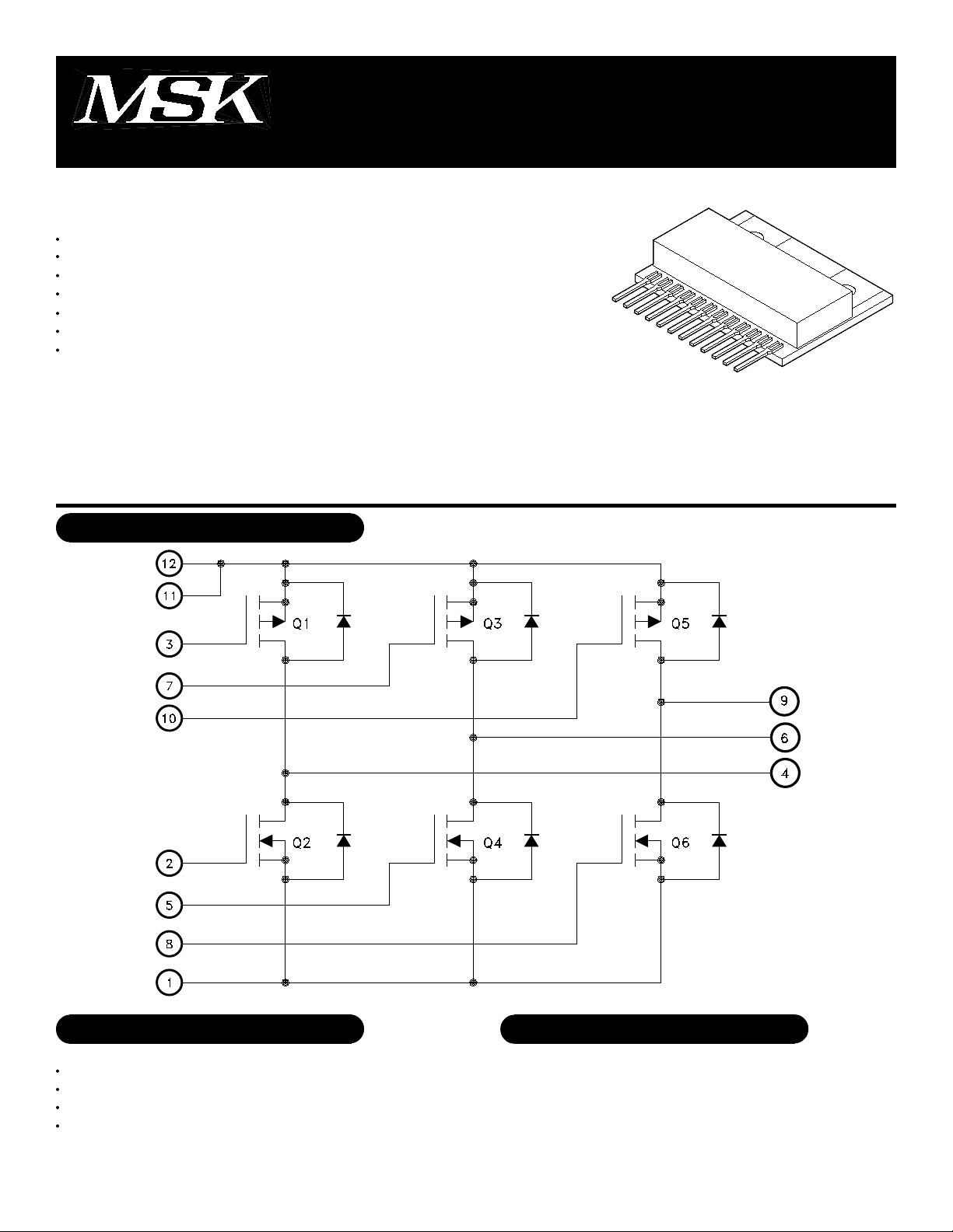
EQUIVALENT SCHEMATIC
TYPICAL APPLICATIONS
Three Phase Brushless DC Motor Servo Control
Disk Drive Spindle Control
Fin Actuator Control
Az-El Antenna Control
PIN-OUT INFORMATION
Source 2,4,6
1
Gate 2
2
Gate 1
3
Drain 1,2
4
Gate 4
5
Drain 3,4
6
1 Rev. A 7/00
Source 1,3,5
12
Source 1,3,5
11
Gate 5
10
Drain 5,6
9
Gate 6
8
Gate 3
7

ABSOLUTE MAXIMUM RATINGS
VDSS
VDGDR
VGS
ID
IDM
RTH-JC
Drain to Source Voltage
○○○○○○○○○○○
Drain to Gate Voltage
(RGS=1MΩ)
○○○○○○○○○○○○○○○○○
Gate to Source Voltage (Continuous)
Continuous Current (N-Channel)
(P-Channel)
Pulsed Current (N-Channel)
(P-Channel)
○○○○○○○○○
○○○○○○○○○
Thermal Resistance (Junction to Case)
(N-Channel FETs)
(P-Channel FETs)
○○○○○○○○○○○○○○○○
○○○○○○○○○○○○○○○○
ELECTRICAL SPECIFICATIONS
○○○
±20V MAX
○○○○○○
○○○○○○○
55V MAX
55V MAX
30A MAX
14A MAX
40A MAX
20A MAX
2°C/W
6°C/W
Single Pulse Avalanche Energy
(Q2,Q4,Q6)
(Q1,Q3,Q5)
Junction Temperature
TJ
Storage Temperature
TST
Case Operating Temperature Range
TC
Lead Temperature Range
TLD
(10 Seconds)
○○○○○○○○○○○○○○○○○○○
○○○○○○○○○○○○○○○○○○○
○○○○○○○○○○
○○○○○○○○
○○○○○○○○○○○○○○○
570mJ
180mJ
+175°C MAX
-55°C to +150°C
-55°C to +125°C
300°C MAX
Parameter
Test Conditions
4
Min.
Drain-Source Breakdown Voltage
Drain-Source Leakage Current
Gate-Source Leakage Current
Gate-Source Threshold Voltage
2
Drain-Source On Resistance
Drain-Source On Resistance
Forward Transconductance
N-Channel (Q2,Q4,Q6)
Total Gate Charge
Gate-Source Charge
Gate-Drain Charge
Turn-On Delay Time
Rise Time
Turn-Off Delay Time
Fall Time
Input Capacitance
Output Capacitance
Reverse Transfer Capacitance
P-CHANNEL (Q1,Q3,Q5)
Total Gate Charge
Gate-Source Charge
Gate-Drain Charge
Turn-On Delay Time
Rise Time
Turn-Off Delay Time
Fall Time
Input Capacitance
Output Capacitance
Reverse Transfer Capacitance
BODY DIODE
Forward On Voltage
Reverse Recovery Time
Reverse Recovery Charge
NOTES:
This parameter is guaranteed by design but need not be tested. Typical parameters are representative of actual device performance but are for reference only.
1
Resistance as seen at package pins.
2
Resistance for die only; use for thermal calculations.
3
TA=25°C unless otherwise specified.
4
Test limits due to autotest fixturing constraints.
5
1
1
1
1
1
1
1
1
1
1
1
1
1
1
1
1
1
1
1
5
3
1
1
1
1
1
VGS=0 ID=0.25mA (All Transistors)
DS=55V VGS=0V (Q2,Q4,Q6)
V
DS=-55V VGS=0V (Q1,Q3,Q5)
V
GS=±20V VDS=0 (All Transistors)
V
DS=VGS ID=250µA (Q2,Q4,Q6)
V
DS=VGS ID=250µA (Q1,Q3,Q5)
V
GS=10V ID=10A (Q2,Q4,Q6)
V
GS=-10V ID=-10A (Q1,Q3,Q5)
V
GS=10V ID=10A (Q2,Q4,Q6)
V
GS=10V ID=-10A (Q1,Q3,Q5)
V
DS=25V ID=10A (Q2,Q4,Q6)
V
DS=-25V ID=-10A (Q1,Q3,Q5)
V
D=30A
I
DS=44V
V
GS=10V
V
DD=28V
V
D=30A
I
G=2.5Ω
R
D=0.93Ω
R
GS=0V
V
DS=25V
V
f=1MHz
D=-10A
I
DS=-44V
V
GS=-10V
V
DD=-28V
V
D=-10A
I
G=13Ω
R
D=2.6Ω
R
GS=0V
V
DS=-25V
V
f=1MHz
S=30A VGS=0V (Q2,Q4,Q6)
I
S=-10A VGS=0V (Q1,Q3,Q5)
I
S=30A di/dt=100A/µS (Q2,Q4,Q6)
I
S=-10A di/dt=100A/µS (Q1,Q3,Q5)
I
S=30A di/dt=100A/µS (Q2,Q4,Q6)
I
S=-10A di/dt=100A/µS (Q1,Q3,Q5)
I
2
55
-
-
-
2.0
-2.0
-
-
-
-
30
4.2
-
-
-
-
-
-
-
-
-
-
-
-
-
-
-
-
-
-
-
-
-
-
-
-
-
-
MSK3018
Typ.
-
-
-
-
-
-
-
-
-
-
-
-
-
-
-
14
62
47
58
3400
830
240
-
-
-
13
55
130
41
620
280
140
1.3
-1.6
120
54
510
110
Max.
-
25
-25
±100
4.5
-4.5
0.04
0.16
0.013
0.10
-
-
150
24
55
-
-
-
-
-
-
-
35
7.9
16
-
-
-
-
-
-
-
-
-
190
82
760
160
Rev. A 7/00
Units
V
µA
µA
nA
V
V
Ω
Ω
Ω
Ω
S
S
nC
nC
nC
nS
nS
nS
nS
pF
pF
pF
nC
nC
nC
nS
nS
nS
nS
pF
pF
pF
V
V
nS
nS
nC
nC
 Loading...