

MSK MSK3017 Datasheet
ISO-9001 CERTIFIED BY DSCC
THREE PHASE BRIDGE
MOSFET POWER MODULE
3017
M.S.KENNEDY CORP.
4707 Dey Road Liverpool, N.Y. 13088 (315) 701-6751
FEATURES:
All N-Channel Mosfets
Isolated Package for Direct Heat Sinking, Excellent Thermal Conductivity
Avalanche Rated Devices
Interfaces with Most Brushless Motor Drive IC's
200 Volt, 30 Amp Full Three Phase Bridge at 25°C
DESCRIPTION:
The MSK 3017 is an all N-Channel three phase power MOSFET Bridge Circuit. Packaged in a space efficient isolated
ceramic tab power SIP that allows for direct heat sinking, the MSK 3017 can be interfaced with a wide array of brushless
motor drive IC's. The MSK 3017 uses M.S Kennedy's proven power hybrid technology to produce a cost effective high
performance circuit for use in today's sophisticated servo motor and disk drive systems.
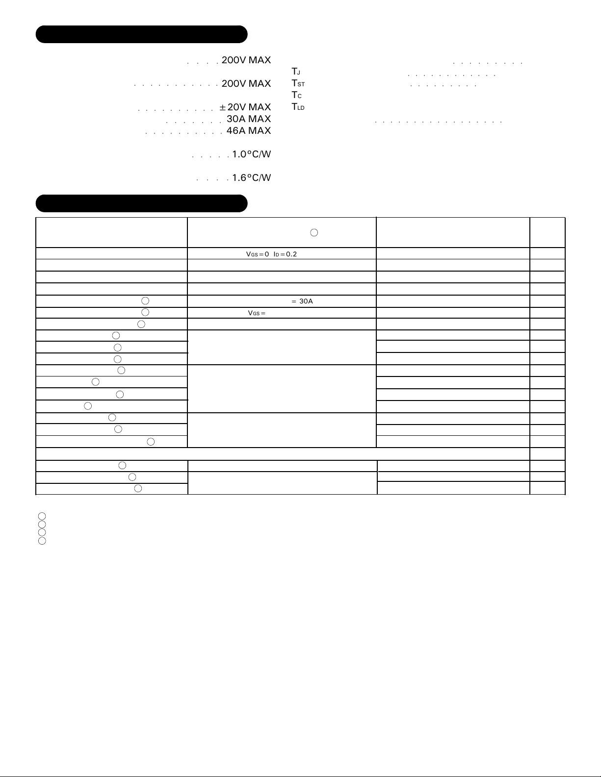
EQUIVALENT SCHEMATIC
TYPICAL APPLICATIONS
Three Phase Brushless DC Motor Servo Control
Disk Drive Spindle Control
Fin Actuator Control
Az-El Antenna Control
PIN-OUT INFORMATION
1
Drain Q2, Q4, Q6
2
Drain Q2, Q4, Q6
3
Drain Q2, Q4, Q6
4
Gate Q2
5
Gate Q1
6
Drain Q1, Source Q2
7
Drain Q1, Source Q2
8
Drain Q1, Source Q2
9
Gate Q4
10
Gate Q3
11
Drain Q3, Source Q4
1 Rev. - 8/01
Drain Q3,Source Q4
12
Drain Q3, Source Q4
13
Source Q1, Q3, Q5
14
Source Q1, Q3, Q5
15
Source Q1, Q3, Q5
16
Gate Q6
17
Drain Q5, Source Q6
18
Drain Q5, Source Q6
19
Drain Q5, Source Q6
20
Gate Q5
21
ABSOLUTE MAXIMUM RATINGS
VDSS
VDGDR
VGS
ID
IDM
RTH-JC
Drain to Source Voltage
Drain to Gate Voltage
(RGS=1MΩ)
○○○○○○○○○○○
Gate to Source Voltage
(Continuous)
Continuous Current
Pulsed Current
○○○○○○○○○○
○○○○○○○
○○○○○○○○○○
Thermal Resistance
(Junction to Case)@25°C
RTH-JC
Thermal Resistance
(Junction to Case)@125°C
ELECTRICAL SPECIFICATIONS
Parameter
Drain-Source Breakdown Voltage
Drain-Source Leakage Current
Gate-Source Leakage Current
Gate-Source Threshold Voltage
Drain-Source On Resistance
Drain-Source On Resistance
Forward Transconductance
Total Gate Charge
Gate-Source Charge
Gate-Drain Charge
Turn-On Delay Time
Rise Time
Turn-Off Delay Time
Fall Time
Input Capacitance
Output Capacitance
Reverse Transfer Capacitance
Body Diode
Forward On Voltage
Reverse Recovery Time
Reverse Recovery Charge
1
1
1
2
3
1
1
1
1
1
1
1
1
1
1
1
○○○○
±20V MAX
○○○○○
○○○○
200V MAX
200V MAX
30A MAX
46A MAX
1.0°C/W
1.6°C/W
Test Conditions
VGS=0 ID=0.25mA
DS=200V VGS=0V
V
GS=±20V VDS=0
V
DS=VGS ID=250µA
V
GS=10V ID = 30A
V
GS=10V ID=30A
V
DS=50V ID=30A
V
D = 30A
I
DS=160V
V
GS = 10V
V
DD=100V
V
D = 30A
I
G = 4.3Ω
R
RD = 2.1Ω
VGS=0V
DS=25V
V
f=1MHz
S=30 A VGS=0V
I
S=30 A di/dt=100A/µS
I
Single Pulse Avalanche Energy
Junction Temperature
TJ
Storage Temperature
TST
Case Operating Temperature Range
TC
Lead Temperature Range
TLD
(10 Seconds)
4
○○○○○○○○○○○○○○○○○
○○○○○○○○○○○○
○○○○○○○○○
MSK3017
Min.
200
-
-
2.0
-
-
24
-
-
-
-
-
-
-
-
-
-
-
-
-
○○○○○○○○○
-55°C to +150°C
-55°C to +125°C
Typ.
-
-
-
-
-
-
-
-
-
-
23
120
100
94
5200
1200
310
1.8
390
4.8
Max.
250
±100
0.09
0.06
230
110
590
1000 mJ
+150°C MAX
300°C MAX
Units
-
4.0
-
42
-
-
-
-
-
-
-
-
7.2
V
µA
nA
V
Ω
Ω
S
nC
nC
nC
nS
nS
nS
nS
pF
pF
pF
V
nS
µC
NOTES:
1
This parameter is guaranteed by design but need not be tested. Typical parameters are representative of actual device performance but are for reference only.
2
Resistance as seen at package pins.
3
Resistance for die only; use for thermal calculations.
4
TA=25°C unless otherwise specified.
2 Rev. - 8/01
 Loading...