


MSK MSK3013 Datasheet
ISO-9001 CERTIFIED BY DSCC
QUAD N-CHANNEL
MOSFET POWER MODULE
M.S.KENNEDY CORP.
4707 Dey Road Liverpool, N.Y. 13088
FEATURES:
• Pin Compatible with MPM3013
• QUAD Independent N - Channel MOSFETS
• Isolated Package for Direct Heat Sinking, Excellent Thermal Conductivity
• Avalanche Rated Devices
• 55 Volt, 25 Amp Rated
• Low RDS (ON) - 0.022Ω For Each Die
DESCRIPTION:
The MSK 3013 is a QUAD N-Channel power circuit packaged in a space efficient isolated ceramic tab power SIP
package. The MSK 3013 consists of four totally isolated N-Channel MOSFETs. The MSK 3013 uses M.S.Kennedy's
proven power hybrid technology to bring a cost effective high performance circuit for use in today's sophisticated
servo motor and disk drive systems. The MSK 3013 is a replacement for the MPM3013 with only minor differences
in specifications.
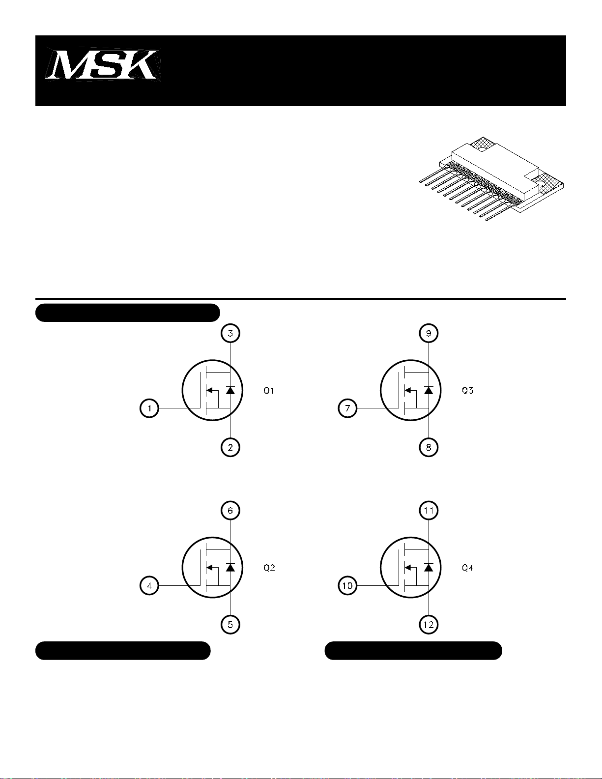
EQUIVALENT SCHEMATIC
3013
(315) 701-6751
TYPICAL APPLICATIONS
• Stepper Motor Servo Control
• Disk Drive Head Control
• X-Y Table Control
• Az-El Antenna Control
• Various Switching Applications
PIN-OUT INFORMATION
1 Q1 Gate 7 Q3 Gate
2 Q1 Source 8 Q3 Source
3 Q1 Drain 9 Q3 Drain
4 Q2 Gate 10 Q4 Gate
5 Q2 Source 11 Q4 Drain
6 Q2 Drain 12 Q4 Source
1
Rev. B 7/00
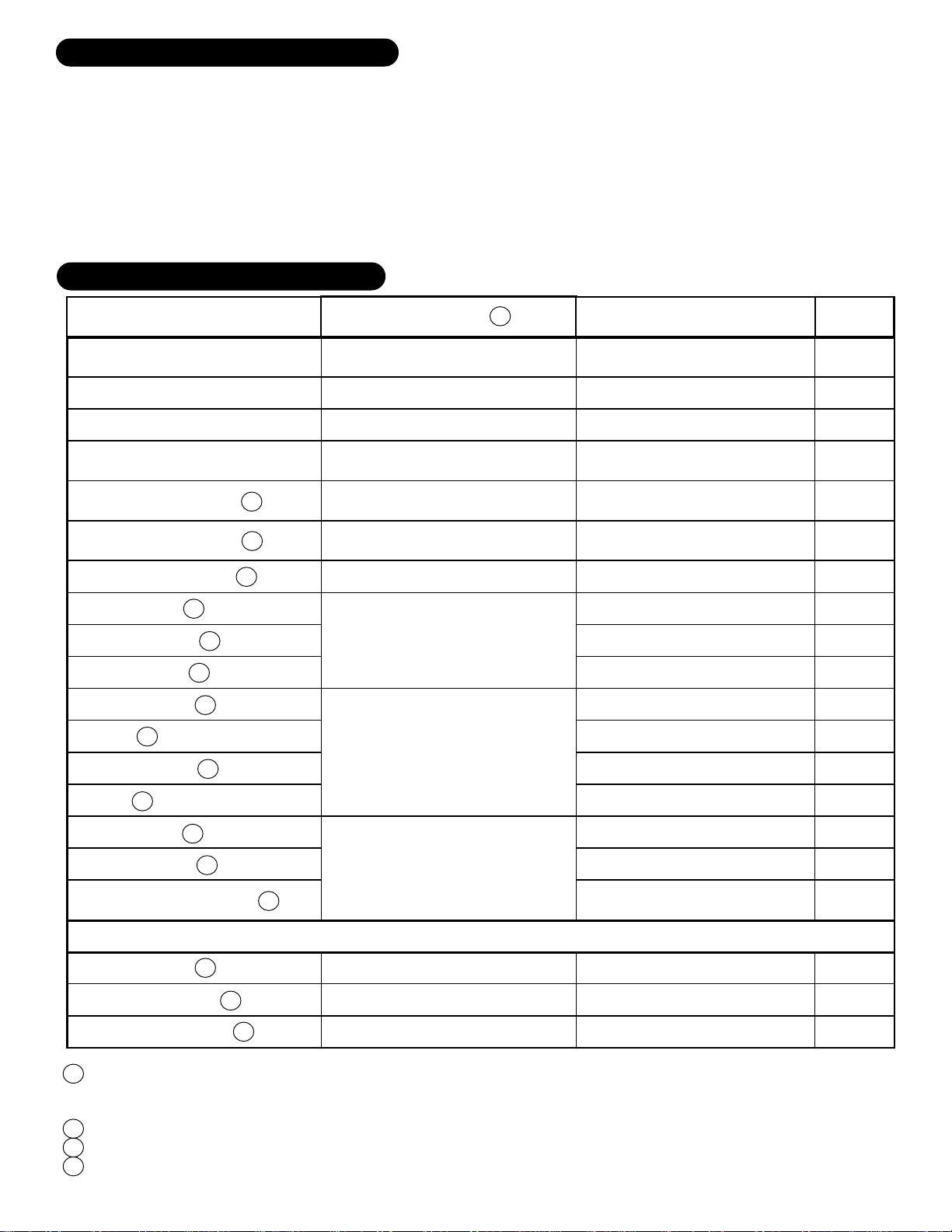
ABSOLUTE MAXIMUM RATINGS
VDSS Drain to Source Voltage . . .55V MAX
VDGDR Drain to Gate Voltage
(RGS=1MΩ)......... 55V MAX
VGS Gate to Source Voltage
(Continuous)........ ±20V MAX
TJ Junction Temperature. . . ........+175°C MAX
TST Storage Temperature. . . ......-55°C TO +150°C
TC Case Operating Temperature Range . .-55°C TO 125°C
TLD Lead Temperature Range
(10 Seconds) . . . . . . ..........300°C MAX
ID Continuous Current ..... 25A MAX
IDM Pulsed Current ....... 49A MAX
RTH-JC Thermal Resistance
(Junction to Case)...... 0.3°C/W
ELECTRICAL SPECIFICATIONS
Parameter
Drain-Source Breakdown Voltage VGS = 0 ID = 0.25 mA 55 - - V
Drain-Source Leakage Current VDS = 55V VGS = 0V - - 25 µA
Gate-Source Leakage Current VGS = ±20V VDS = 0 - - ±100 nA
Gate-Source Threshold Voltage VDS = VGS ID = 250 µA 2 - 4 V
Drain-Source on Resistance 2 VGS = 10V ID = 25A - 0.033 0.040
Drain-Source on Resistance 3 VGS = 10V ID = 25A - - 0.022
Test Conditions 4
Min. Typ. Max.
MSK 3013
Units
Ω
Ω
Forward Transconductance 1 VDS = 25V ID = 25A 17 - - S
Total Gate Charge 1 ID = 25A - - 65 nC
Gate-Source Charge 1 VDS = 28V - - 12 nC
Gate-Drain Charge 1 VGS = 10V - - 27 nC
Turn-On Delay Time 1 VDD = 28V - 7.3 - nS
Rise Time 1 ID = 25A - 69 - nS
Turn-Off Delay Time 1 RG = 12 - 47 - nS
Fall Time 1 RD = 1.1 - 60 - nS
Input Capacitance 1 VGS = 0V - 1300 - pF
Output Capacitance 1 VDS = 25V - 410 - pF
Reverse Transfer Capacitance 1 f = 1 MHz - 150 - pF
BODY DIODE
Forward on Voltage 1 IS = 25A VGS = 0V - 1.3 1.75 V
Reverse Recovery Time 1 IS = 25A di/dt = 100A/µS - 65 98 nS
Ω
Reverse Recovery Charge 1 IS = 25A di/dt = 100A/µS - 160 240 µC
NOTES:
1 This parameter is guaranteed by design but need not be tested. Typical parameters are representative of
actual
device performance but are for reference only.
2 Resistance as seen at package pins.
3 Resistance for die only; use for thermal calculations.
4TA=25°C unless otherwise specified. Parameters apply to each transistor in the module.
2
Rev. B 7/00