

MSK MSK3004 Datasheet
H-BRIDGE
ISO-9001 CERTIFIED BY DSCC
MOSFET POWER MODULE
3004
M.S.KENNEDY CORP.
4707 Dey Road Liverpool, N.Y. 13088 (315) 701-6751
FEATURES:
Pin Compatible with MPM3004
P and N Channel MOSFETs for Ease of Drive
Isolated Package for Direct Heat Sinking, Excellent Thermal Conductivity
Avalanche Rated Devices
55 Volt, 10 Amp Full H-Bridge
DESCRIPTION:
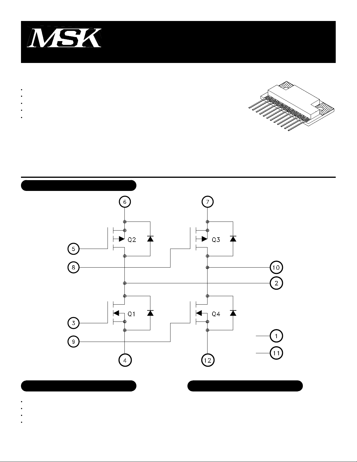
The MSK 3004 is an H-bridge power circuit packaged in a space efficient isolated ceramic tab power SIP package.
The MSK 3004 consists of P-Channel MOSFETs for the top transistors and N-Channel MOSFETs for the bottom
transistors. The MSK 3004 uses M.S.Kennedy's proven power hybrid technology to bring a cost effective high
performance circuit for use in today's sophisticated servo motor and disk drive systems. The MSK 3004 is a
replacement for the MPM3004 with only minor differences in mechanical specifications.
EQUIVALENT SCHEMATIC
TYPICAL APPLICATIONS
Stepper Motor Servo Control
Disk Drive Head Control
X-Y Table Control
Az-El Antenna Control
PIN-OUT INFORMATION
N/C
1
Drain 1,2
2
Gate 1
3
Source 1
4
Gate 2
5
Source 2
6
1
12
11
10
9
8
7
Source 4
N/C
Drain 3,4
Gate 4
Gate 3
Source 3
Rev. F 6/00
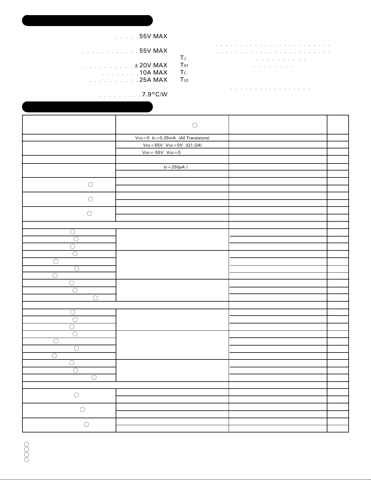
ABSOLUTE MAXIMUM RATINGS
VDSS
VDGDR
VGS
ID
IDM
RTH-JC
Drain to Source Voltage
Drain to Gate Voltage
(RGS=1MΩ)
○○○○○○○○○○○○
Gate to Source Voltage
(Continuous)
Continuous Current
Pulsed Current
○○○○○○○○○○
○○○○○○○○
○○○○○○○○○○
Thermal Resistance
(Junction to Case)
○○○○○○○○○
○○○○○
±20V MAX
55V MAX
55V MAX
10A MAX
25A MAX
7.9°C/W
Single Pulse Avalanche Energy
(Q1,Q4)
(Q2,Q3)
Junction Temperature
TJ
Storage Temperature
TST
Case Operating Temperature Range
TC
Lead Temperature Range
TLD
(10 Seconds)
○○○○○○○○○○○○○○○○○○○○○○○○
○○○○○○○○○○○○○○○○○○○○○○○○
○○○○○○○○○○
○○○○○○○○
○○○○○○○○○○○○○○○○○
+175°C MAX
-55°C to +150°C
-55°C to +125°C
300°C MAX
ELECTRICAL SPECIFICATIONS
Parameter
Drain-Source Breakdown Voltage
Drain-Source Leakage Current
Gate-Source Leakage Current
Gate-Source Threshold Voltage
Drain-Source On Resistance
Drain-Source On Resistance
Forward Transconductance
N-Channel (Q1,Q4)
Total Gate Charge
Gate-Source Charge
Gate-Drain Charge
Turn-On Delay Time
Rise Time
Turn-Off Delay Time
Fall Time
Input Capacitance
Output Capacitance
Reverse Transfer Capacitance
P-CHANNEL (Q2,Q3)
Total Gate Charge
Gate-Source Charge
Gate-Drain Charge
Turn-On Delay Time
Rise Time
Turn-Off Delay Time
Fall Time
Input Capacitance
Output Capacitance
Reverse Transfer Capacitance
BODY DIODE
Forward On Voltage
Reverse Recovery Time
Reverse Recovery Charge
1
1
1
1
1
1
1
2
3
1
1
1
1
1
1
1
1
1
1
1
1
1
1
1
Test Conditions
4
Min.
VGS=0 ID=0.25mA (All Transistors)
DS=55V VGS=0V (Q1,Q4)
V
DS=-55V VGS=0V (Q2,Q3)
V
GS=±20V VDS=0 (All Transistors)
V
DS=VGS ID=250µA (Q1,Q4)
V
DS=VGS ID=250µA (Q2,Q3)
V
GS=10V ID=10A (Q1,Q4)
V
GS=-10V ID=-7.2A (Q2,Q3)
V
GS=10V ID=10A (Q1,Q4)
V
GS=10V ID=-7.2A (Q2,Q3)
V
DS=25V ID=10A (Q1,Q4)
V
DS=-25V ID=-7.2A (Q2,Q3)
V
D=10A
I
DS=44V
V
GS=10V
V
DD=28V
V
D=10A
I
G=24Ω
R
D=2.6Ω
R
GS=0V
V
DS=25V
V
1
1
S=-7.2A VGS=0V (Q2,Q3)
I
S=10A di/dt=100A/µS (Q1,Q4)
I
S=-7.2A di/dt=100A/µS (Q2,Q3)
I
S=10A di/dt=100A/µS (Q1,Q4)
I
S=-7.2A di/dt=100A/µS (Q2,Q3)
I
f=1MHz
D=-7.2A
I
DS=-44V
V
GS=-10V
V
DD=-28V
V
D=-7.2A
I
G=24Ω
R
D=3.7Ω
R
GS=0V
V
DS=-25V
V
f=1MHz
S=10A VGS=0V (Q1,Q4)
I
55
-
-
-
2.0
-2.0
-
-
-
-
4.5
2.5
-
-
-
-
-
-
-
-
-
-
-
-
-
-
-
-
-
-
-
-
-
-
-
-
-
-
MSK3004
Typ.
-
-
-
-
-
-
-
-
-
-
-
-
-
-
-
4.9
34
19
27
370
140
65
-
-
-
13
55
23
37
350
170
92
1.3
-1.6
56
47
0.12
0.084
Max.
-
25
-25
±100
4.5
-4.5
0.15
0.28
0.07
0.175
-
-
20
5.3
7.6
-
-
-
-
-
-
-
19
5.1
10
-
-
-
-
-
-
-
-
-
83
71
0.18
0.13
NOTES:
1
This parameter is guaranteed by design but need not be tested. Typical parameters are representative of actual device performance but are for reference only.
2
Resistance as seen at package pins.
3
Resistance for die only; use for thermal calculations.
4
TA=25°C unless otherwise specified.
2
Rev. F 6/00
71mJ
96mJ
Units
V
µA
µA
nA
V
V
Ω
Ω
Ω
Ω
S
S
nC
nC
nC
nS
nS
nS
nS
pF
pF
pF
nC
nC
nC
nS
nS
nS
nS
pF
pF
pF
V
V
nS
nS
µC
µC
 Loading...