

MSK MSK2541B, MSK2541 Datasheet

ISO 9001 CERTIFIED BY DSCC
DUAL HIGH POWER
M.S. KENNEDY CORP
4707 Dey Road Liverpool, N.Y. 13088 (315) 701-6751
FEATURES:
Available as SMD #5962-9083801 HX
High Output Current - 10 Amps Peak
Wide Power Supply Range - ±10V to ±40V
On Board Current Limit
FET Input
Isolated Case
Second Source for OMA 2541SKB
DESCRIPTION:
The MSK 2541 is a high power dual monolithic amplifier ideally suited for high power amplification and magnetic
deflection applications. This amplifier is capable of operation at a supply voltage rating of 80 volts and can deliver
guaranteed continuous output currents up to 5A per amplifier. The MSK 2541 has internal current limit circuitry to
protect the amplifier and load from transients. The MSK 2541 is available in a hermetically sealed 8 pin TO3 package
that is isolated from internal circuitry. This allows for convenient bolt down heat sinking when necessary.
EQUIVALENT SCHEMATIC
OP-AMP
MIL-PRF-38534 CERTIFIED
2541
TYPICAL APPLICATIONS
Servo Amplifer
Motor Driver
Audio Amplifier
Programmable Power Supply
Bridge Amplifier
PIN-OUT INFORMATION
1 Output B 8 Inverting Input B
2 Positive Power Supply 7 Non-Inverting Input B
3 Non-Inverting Input A 6 Negative Power Supply
4 Inverting Input A 5 Output A
1
Rev. B 8/00
ABSOLUTE MAXIMUM RATINGS
±V
CC Voltage Supply ±40V
OUT Peak Output Current See S.O.A.
I
IN Differential Input Voltage ±VCC
V
VIN Common Mode Input Voltage ±VCC
TC Case Operating Temperature Range
MSK 2541B -55° to +125°C
MSK 2541 -40° to +85°C
○○○○○○○○○○○○
○○○○○○○
○○○○○○○
○○○○○
○○○○○○○○○○○○
○○○○○○○○○○○○
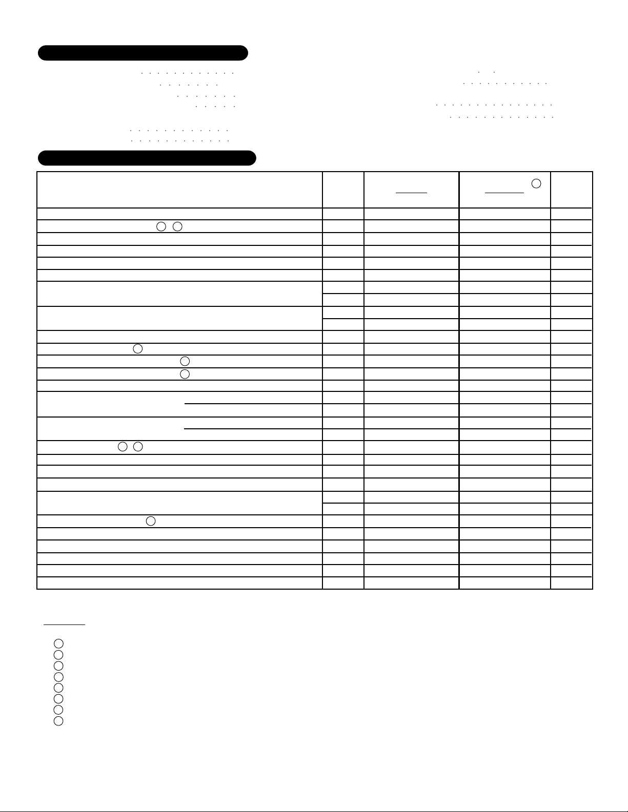
ELECTRICAL SPECIFICATIONS
Parameter
STATIC
Supply Voltage Range
Quiescent Current
2
Total - Both Amplifiers V
INPUT
Input Offset Voltage
Input Offset Voltage Drift
Input Bias Current
Input Bias Current
Input Capacitance
Input Impedance
Common Mode Rejection Ratio
Power Supply Rejection Ratio
4
F = DC V
V
OUTPUT
Output Voltage Swing
Output Current
4
Settling Time
3
Power Bandwidth
TRANSFER CHARACTERISTICS
Slew Rate
Open Loop Voltage Gain
THERMAL RESISTANCE
4
θJC (Junction to Case)
θJC
One Amplifier, AC Output F > 60 Hz
θJC
θJC
Both Amplifiers, AC Output F > 60 Hz
θJA (Junction to Ambient)
Test Conditions
4
IN = 0V
V
V
IN = 0V
V
CM = 0V
Either Input
VCM = 0V
F = DC
4
CC = ±10V to ±40V
4
L = 5.6Ω F ≤ 10 KHz
R
R
L = 10Ω F = 10 KHz
R
L = 5.6Ω F ≤ 10 KHz
R
L = 10Ω F = 10 KHz
0.1% 2V step
R
L = 10Ω VO = 20 VRMS
VOUT = ±10V RL = 10Ω
F = 10 Hz R
One Amplifier, DC Output
Both Amplifiers, DC Output
No Heat Sink
IN = 0V
CM = ±22V
L = 10 KΩ
TST Storage Temperature Range -65° to +150°C
TLD Lead Temperature Range 300°C
○○
○○○○○○○○○○○
(10 Seconds)
PD Power Dissipation 125W
TJ Junction Temperature 150°C
MSK 2541B
Group A
Subgroup
-
1, 2, 3
1
2, 3
1
2, 3
1
2, 3
-
-
-
-
4
5, 6
4
5, 6
-
4
4
4
5, 6
-
-
-
-
-
Military Industrial
Min.
±10
Typ.
±35
±40
-
±0.1
-
±15
-
±4
-
±10
-
2.0
-
-
-
10
-
95
±28
±30
±5
113
-
90
±29
±31
±8
±3.0
-
45
6
95
55
10
100
85
-
1.4
-
1.25
-
0.9
-
0.8
-
30
○○○○○○○○○○○○○○○
○○○○○○○○○○○○○
MSK 2541
Max.
±40
±60
±1.0
±30
±50
±50
30
20
-
5
-
12
-
-
-
-
-
-
-
2
-
-
-
-
-
-
-
1.9
1.5
1.2
1.0
-
Min.
±10
-
-
-
-
-
-
-
-
-
90
-
±28
-
±5
-
-
40
6
90
-
-
-
-
-
-
Typ.
±35
±40
±1.0
±15
±10
±29
1.25
±4
2.0
5
10
113
90
±8
2
50
10
100
1.4
0.9
0.8
30
5
Max.
±40
±60
±10
±100
-
12
-
-
-
30
1.9
1.5
1.2
1.0
Units
V
mA
mV
-
µV/°C
pA
-
nA
pA
-
nA
-
-
-
-
-
-
-
-
-
-
-
-
-
pF
W
dB
dB
V
V
A
A
µS
KHz
V/µS
dB
dB
°C/W
°C/W
°C/W
°C/W
-
°C/W
NOTES:
1 Unless otherwise specified: RCL = 0Ω, ±VCC = ±34 VDC, all specs are per amplifier.
2 Electrical specifications are derated for power supply voltages other than ±34 VDC.
3 AV = -1, measured in false summing junction circuit.
4 Devices shall be capable of meeting the parameter, but need not be tested. Typical parameters are for reference only.
5 Industrial grade devices shall be tested to subgroups 1 and 4 unless otherwise specified.
6 Military grade devices ('B' suffix) shall be 100% tested to subgroups 1, 2, 3 and 4.
7 Subgroup 5 and 6 testing available upon request.
8 Subgroup 1, 4 TA=TC=+25°C
Subgroup 2, 5 TA=TC=+125°C
Subgroup 3, 6 TA=TC=-55°C
2
Rev. B 8/00
 Loading...