

MSK MSK1932U-0, MSK1932S-4, MSK1932S-0, MSK1932D-4, MSK1932D-0 Datasheet
...
ISO-9001 CERTIFIED BY DSCC
ULTRA HIGH SPEED/VOLTAGE
1932
VIDEO AMPLIFIER
M.S.KENNEDY CORP.
4707 Dey Road Liverpool, N.Y. 13088 (315) 701-6751
SERIES
FEATURES:
Low Cost Complete Amplifier System
100Vpp Output Signal Into 10pF
Ultra Fast Transition Times: 1.7nS @ 50Vpp
User Adjustable Contrast and Brightness
TTL Compatible Blanking
On Board DC Reference Output
Customized Versions Readily Available
Available with Three Lead Bend Options
MIL-PRF-38534 CERTIFIED
DESCRIPTION:
The MSK 1932 Series of High Speed, High Voltage Video Amplifiers is designed to directly drive the cathode of
today's high performance CRT's. The MSK 1932 has user adjustable contrast and brightness levels and also comes
with a blanking function. The MSK 1932 can be directly connected to many video sources including RS170, RS343
and high speed video D/A converters. The MSK 1932 is available in four versions for different applications. The MSK
1932-0 has no internal high voltage resistor or inductor allowing the user to dissipate much of the power externally.
The MSK 1932-2, MSK 1932-4 and the MSK 1932-6 each have an internal resistor-inductor designed for optimum
bandwidth. The MSK 1932-6 has slightly lower bandwidth but can be operated from up to +130V. Each version of
the MSK 1932 is packaged in an isolated 22 pin insulated ceramic substrate that can be directly connected to a heat
sink using standard mounting techniques. The leads are available straight out, bent up or bent down.
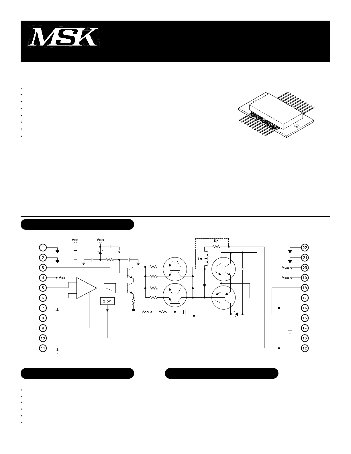
EQUIVALENT SCHEMATIC
TYPICAL APPLICATIONS
Helmet Mounted Displays
High Resolution RGB Displays
High Resolution Monochrome Displays
Automatic Test Equipment
Medical Monitors
CAE/CAD Station Monitors
PIN-OUT INFORMATION
1
2
3
4
5
6
7
8
Ground
Ground
Blank
VEE
-Input
+Input
Ground
VGain
9
10
11
12
13
14
15
16
Voff
Vref
Ground
+VHV RES
+VHV RES
Ground
+VHV
+VHV
17
18
19
20
21
22
Output
Cath Rtn
Vcc
Vcc
Ground
Ground
Rev. B 8/001
ABSOLUTE MAXIMUM RATINGS
+VHV
High Voltage Supply (1932-0)
(1932-2)
(1932-4)
(1932-6)
VCC
VEE
VIN
VIC
VGAIN
VOFF
Positive Supply Voltage
Negative Supply Voltage
Differential Input Voltage
Common Mode Input Voltage
Gain Adjust Input Voltage
Offset Adjust Input Voltage
ELECTRICAL SPECIFICATIONS
Parameter
STATIC
Quiescent Current
High Voltage Supply
Thermal Resistance to Case
INPUT
Input Bias Current
Blank Input Current
Offset Adjust Input Current
Gain Adjust Input Current
Blank Input Pulse Width
Common Mode Rejection Ratio
Input Impedance
Input Capacitance
Blank Mode Input
Rejection ∆V
Gain Adjust Rejection ∆V
Power Supply Rejection Ratio
Internal Rp
OUTPUT
Reference Output Voltage
∆V Blank Mode
∆V Min Offset
∆V Max Offset
Voltage Gain
Output Voltage High
Output Voltage Low
Transistion Times
Linearity Error
Gain Linearity
Thermal Distortion
6
2
3
6
6
7
3
3
3
3
4
3
4
6
4
5
6
5
5
6
3
3
∆V=VHV-VOUT VOFF=0V VGAIN=3V
6
6
6
6
7
VGAIN =4V VOFF=1V VCM=0.5V
3
○○○○
○○○○○
○○○○○
○○○○○
○○○○○○○○○
○○○○○○○○○
○○○○○○○○○
○○○○○○
-0.6 to +6V
○○○○
-0.6 to +6V
○○○
Test Conditions
VCM=0V @ +15V
VCM=0V @ -10.5V
QOUT and QCAS
3
VCM=0V
VBLANK=0.4V
VBLANK=2.4V
7
3
4
+VCC and -VEE=Nom ±5%
3
VBLANK=2.4V VGAIN=5V
VOFF=1V VIN=2.0V VCM=0.5V
VOFF=1V
VGAIN=5V
Normal Operation
VCM=±0.5V F=10Hz
Either Input F=DC
Either Input
VBLANK=2.4V VIN=0.3V
∆V=VHV-VOUT
∆VGAIN=5V
IOUT<2mA
∆V=VHV-VOUT VOFF=1V
∆V=VHV-VOUT VOFF=5V
VIN=0.6V F=10KHz
VGAIN=3V Both Inputs
VGAIN=3V F=10KHz
VGAIN=3V F=10KHz
VIN=0.6V TR=TF<0.5nS
1
+110V
+110V
+75V
+130V
+17V
-12V
2V
±2V
Min.
30
30
10K
25
5.2
32
95
VBLANK
IREF
TST
TLD
TJ
IRP
TC
MSK1932-0
Typ.
75
-
-75
-
100
10
-
±1
-
500
-
300
-
2
-
2
-
-
40
-
20K
2
-
-
-
30
0
-
5.5
3
0
42
98
10
-
3.5
-
-
-
-
-
-
-
Blank Input Voltage
Reference Output Current
Storage Temperature Range
Lead Temperature Range
(10 Seconds)
Junction Temperature
Current Through Rp
Case Operating Temperature
(All Devices)
MSK1932-2
Max.
Min.
100
-
-100
-
110
30
13
-
±50
-
600
-
400
-
10
-
10
-
-
30
-
-
-
10K
-
-
-
-
25
-
380
5.8
5.2
3xRpRp-3xRp 3xRpRp-3xRp
6
0
52
32
-
95
20
-
4.5
-
±2
-
±2
-
±2
-
Typ.
75
-75
100
10
±1
500
300
2
2
-
40
20K
2
-
30
400
5.5
3
42
98
10
2.8
-
-
-
Max.
100
-100
110
13
±50
600
400
10
10
-
-
-
-
-
420
5.8
6
52
1381107213811072
-
20
4.0
±2
±2
±2
Min.
10K
190
5.2
36
○○○○○○○○○
○○○○○○○○○○
○○○○○○○○○
○○○○○○○○○○○
○○○○○○○○○○○○
MSK1932-4
Max.
Typ.
75
-75
70
10
±1
500
300
2
2
-
40
20K
2
-
30
200
5.5
3
21
68
10
1.7
-
-
-
100
-100
75
13
±50
600
400
10
10
-
-
-
-
±10xRp±10xRp±10xRp3
-
210
5.8
3xRpRp-3xRp
6
26
6855
-
20
2.5
±2
±2
±2
-
-
30
-
-
-
-
-
-
30
-
-
-
25
0
16
65
-
-
-
-
-
-0.6 to +6V
5mA
-40°C to +150°C
300°C
150°C
290mA
-25°C to +125°C
MSK1932-6
Units
Max.
Typ.
Min.
100
-100
130
12
±50
600
400
10
10
-
-
-
-
-
420
5.8
3xRpRp-3xRp
10
52
145
-
20
8
±2
±2
±2
mA
mA
V
°C/W
µA
µA
µA
µA
µA
nS
dB
Ω
pF
mV
mV
dB
Ω
V
mV
V
V
V/V
V
V
nS
%GS
%
%GS
30
30
10K
25
380
5.2
0
32
72
115
75
-
-75
-
120
8
-
±1
-
500
-
300
-
2
-
2
-
-
40
-
20K
2
-
--±2xRp--±2xRp--±2xRp--±2xRp
±10xRp
-
-
30
400
5.5
3
42
120
118
10
-
6
-
-
-
-
-
-
-
NOTES:
1
+VCC = +15V, -VEE = -10.5V, VBLANK = VGAIN = VOFF = ±VIN = 0V, CL=10pF, TC=25°C unless otherwise specified.
2
VHV=Typical Value for each dash number for all parameters.
3
This parameter is quaranteed by design but need not be tested. Typical parameters are representative of actual device performance but are for reference only.
4
RP=Internal RP except MSK 1932-0. External value = 400Ω unless otherwise specified for the MSK 1932-0.
5
∆V is defined as the difference between +VHV and the output.
6
Parameter is 100% tested on production devices.
7
Parameter is sample tested in accordance with MSK industrial grade quality devices.
2
Rev. B 8/00
 Loading...