

MSK MSK1922 Datasheet
ISO-9001 CERTIFIED BY DSCC
ULTRA HIGH SPEED/VOLTAGE
1922
VIDEO AMPLIFIER
M.S.KENNEDY CORP.
4707 Dey Road Liverpool, N.Y. 13088 (315) 701-6751
SERIES
FEATURES:
Ultra High Performance Complete Amplifier System
50Vpp Output Signal Into 10pF
Ultra Fast Transition Times: 1.2nS @ 50Vpp
User Adjustable Contrast and Brightness
TTL Compatible Blanking
On Board DC Reference Output
Customized Versions Readily Available
MIL-PRF-38534 CERTIFIED
DESCRIPTION:
The MSK 1922 High Speed, High Voltage Video Amplifier is designed to directly drive the cathode of today's high
performance CRT's. The MSK 1922 has user adjustable contrast and brightness levels and also comes with a
blanking function. The MSK 1922 can be directly connected to many video sources including RS170, RS343 and high
speed video D/A converters. The MSK 1922 has an internal resistor-inductor designed for optimum bandwith. The
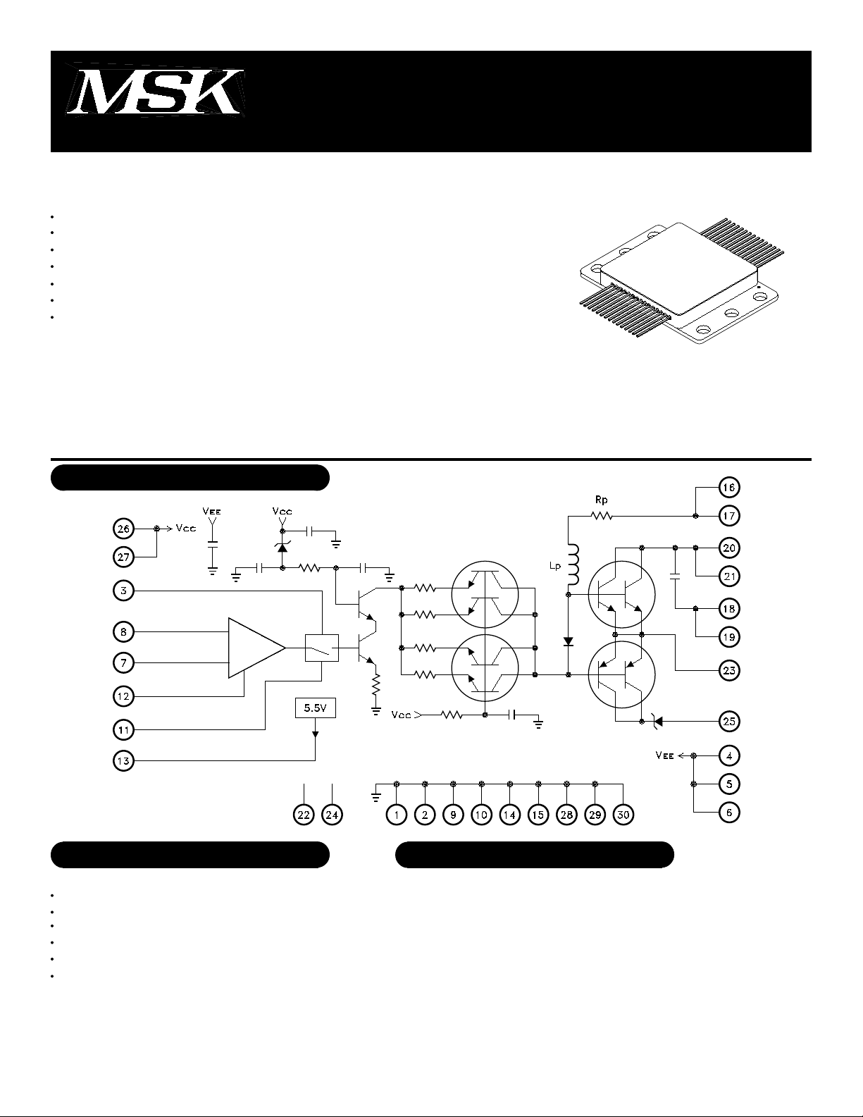
MSK 1922 is packaged in a hermetic 30 pin power flatpack that can be directly connected to a heat sink using
standard 4-40 screws.
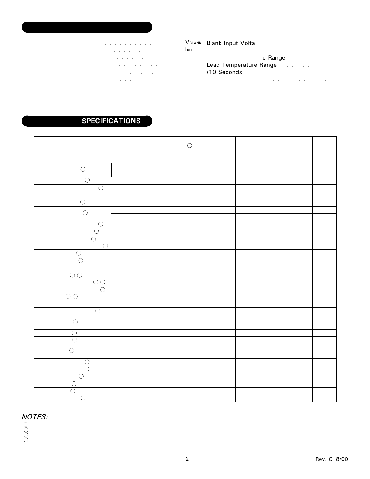
EQUIVALENT SCHEMATIC
TYPICAL APPLICATIONS
Helmet Mounted Displays
High Resolution RGB Displays
High Resolution Monochrome Displays
Automatic Test Equipment
Medical Monitors
CAE/CAD Station Monitors
PIN-OUT INFORMATION
GND
1
GND
2
Blank
3
VEE
4
VEE
5
VEE
6
-Input
7
+Input
8
GND
9
GND
10
1 Rev. C 8/00
11
12
13
14
15
16
17
18
19
20
VGAIN
VOFF
VREF
GND
GND
VHV RES
VHV RES
GND
GND
VHV
VHV
21
N/C
22
Output
23
N/C
24
Cath. RTN/GND
25
VCC
26
VCC
27
GND
28
GND
29
GND
30
ABSOLUTE MAXIMUM RATINGS
+VHV
VCC
VEE
VIN
VIC
VGAIN
VOFF
High Voltage Supply
○○○○○○○○○○
Positive Supply Voltage
Negative Supply Voltage
Differential Input Voltage
Common Mode Input Voltage
Gain Adjust Input Voltage
Offset Adjust Input Voltage
ELECTRICAL SPECIFICATIONS
Parameter
STATIC
Quiescent Current
High Voltage Supply
Thermal Resistance to Case
INPUT
Input Bias Current
Blank Input Current
Offset Adjust Input Current
Gain Adjust Input Current
Blank Input Pulse Width
Common Mode Rejection Ratio
Input Impedance
Input Capacitance
Blank Mode Input
Rejection ∆V
Gain Adjust Rejection ∆V
Power Supply Rejection Ratio
Internal Rp
OUTPUT
Reference Output Voltage
∆V Blank Mode
∆V Min Offset
∆V Max Offset
Voltage Gain
Output Voltage High
Output Voltage Low
Transition Times
Linearity Error
Gain Linearity
Thermal Distortion
4
2
2
2
2
2
2
2
2
2
2
2
3
2
3
2
2
3
4
3
3
3
4
4
4
2
2
2
2
+75V
○○○○○○○○○
○○○○○○○○○
○○○○○○○○○
○○○○○○
○○○○
○○○
∆V=VHV-VOUT VOFF=0V VGAIN=3V
VIN=0.6V TR=TF<0.2nS (input)
VGAIN =4V VOFF=1V VCM=0.5V
VOFF=1V VIN=2.0V VCM=0.5V
+17V
-12V
2V
±2V
-0.6 to +6V
-0.6 to +6V
Test Conditions
VCM=0V @ +15V
VCM=0V @ -10.5V
QOUT and QCAS
VCM=0V
VBLANK=0.4V
VBLANK=2.4V
VOFF=1V
VGAIN=5V
Normal Operation
VCM=±0.5V F=10Hz
Either Input F=DC
Either Input
VBLANK=2.4V VIN=0.3V
∆V=VHV-VOUT
∆VGAIN=5V
+VCC and -VEE=Nom ±5%
IOUT<2mA
∆V=VHV-VOUT VOFF=1V
VBLANK=2.4V VGAIN=5V
∆V=VHV-VOUT VOFF=5V
VIN=0.6V F=10KHz
VGAIN=4V Both Inputs
VGAIN=4V F=10KHz
VGAIN=4V F=10KHz
VBLANK
IREF
TST
TLD
TJ
IRP
TC
1
Blank Input Voltage
○○○○○○○○○
Reference Output Current
Storage Temperature Range
Lead Temperature Range
○○○○○○○○○
(10 Seconds)
Junction Temperature
Current Through Rp
○○○○○○○○○○○
○○○○○○○○○○○○
Case Operating Temperature
MSK1922
Min.
30
30
10K
25
140
5.2
-3xRp Rp 3xRp
11
40
65
Typ.
-
-
-
-
-
-
-
-
-
-
-
-
0
-
-
-
-
-
75
-75
70
10
±1
500
300
2
2
-
40
20K
2
-
-
30
150
5.5
2
16
54 64
68
10
1.2
-
-
-
-0.6 to +6V
○○○○○○○○○○
-40°C to +150°C
300°C
175°C
290mA
-25°C to +125°C
Max.
100
-100
75
13
±50
600
400
10
10
-
-
-
-
±2xRp
±10xRp
-
160
5.8
6
21
-
20
-
±2
±2
±2
Units
mA
mA
V
°C/W
µA
µA
µA
µA
µA
nS
dB
Ω
pF
mV
mV
dB
Ω
V
mV
V
V
V/V
V
V
nS
%GS
%
%GS
5mA
NOTES:
1
+VCC = +15V, -VEE = -10.5V, VBLANK = VGAIN = VOFF = ±VIN = 0V, CL=10pF, TC=25°C unless otherwise specified.
2
This parameter is guaranteed by design but need not be tested. Typical parameters are representative of actual device performance but are for reference only.
3
∆V is defined as the difference between +VHV and the output.
4
Parameter is 100% tested on production devices.
2
Rev. C 8/00
 Loading...