

MSK MSK1911 Datasheet
M.S.KENNEDY CORP.
ISO-9001 CERTIFIED BY DSCC
HIGH PERFORMANCE,
HIGH VOLTAGE
VIDEO DISPLAY DRIVER
1911
4707 Dey Road Liverpool, N.Y. 13088
FEATURES:
Internal Load Resistor for Highest Bandwidth
Ultra Fast Rise Time - 2.0nS Typical
Wide Bandwidth - 225 MHz Typical
Variable Gain - 0 to 100 V/V
On Board Reference Output
60 Vpp Output Voltage Swing
Blanking Capability
User Adjustable Brightness and Contrast
25,000 V/µSec Slew Rate
Low Cost Complete Video CRT Driver System
MIL-PRF-38534 CERTIFIED
(315) 701-6751
DESCRIPTION:
The MSK 1911 is a high performance, high voltage, variable gain video amplifier capable of directly driving high
resolution video displays.
The MSK 1911 features differential inputs and a linearly adjustable gain stage with an output offset adjustment
which allows it to be a versatile performer well suited for many applications. A TTL level blanking input is available to
set the output to a predetermined black level independent of signal input.
The MSK 1911 is packaged in a cost effective, highly thermally conductive, insulated package which can be
bolted directly to a heat sink for efficient thermal management.
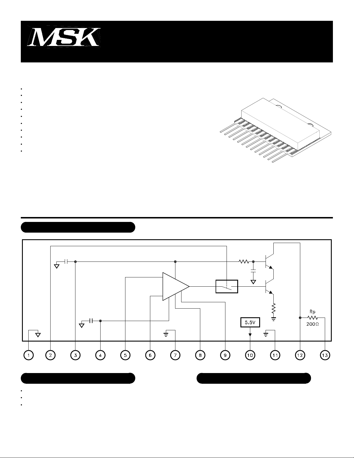
EQUIVALENT SCHEMATIC
TYPICAL APPLICATIONS
High Resolution Mono-Chrome Displays
High Resolution RGB Displays
High Speed, High Voltage Amplification for ATE
PIN-OUT INFORMATION
8
10
11
12
13
9
VGAIN
VOFF
VREF
Ground
Output
+VHV
1
Ground
2
Blank
3
VCC
4
VEE
5
-Input
6
+Input
7
Ground
1 Rev. D 8/00
ABSOLUTE MAXIMUM RATINGS
+VHV
+VCC
-VEE
VID
VGAIN
VOFF
VBLANK
IREF
High Voltage Supply
○○○○○○○○○○○
Positive Supply Voltage
Negative Supply Voltage
Differential Input Voltage
Gain Adjust Input Voltage
Offset Adjust Input Voltage
Blank Input Voltage
○○○○○○○
Reference Output Current
ELECTRICAL SPECIFICATIONS
Parameter
STATIC
Quiescent Current
HIgh Voltage Supply
Thermal Resistance to Case
INPUT
Input Bias Current
Blank Input Current
Offset Adjust Input Current
Gain Adjust Input Current
Blank Input Pulse Width
Common Mode Rejection Ratio
Input Impedance
Input Capacitance
Blank Mode Input Rejection ∆V
Gain Adjust Rejection ∆V
Power Supply Rejection Ratio
OUTPUT
Reference Output Voltage
Output Voltage Blank Mode ∆V
Output Voltage (Min Offset) ∆V
Output Voltage (Max Offset) ∆V
Voltage Gain
Bandwidth
Transition Times
Linearity Error
Gain Linearity
Thermal Distortion
4
2
2
2
2
5
2
5
2
2
2
2
2
2
2
4
4 6
2
4
3
2
2
3
2
2
2
○○○○○○○○○○
○○○○○○○○○○
○○○○○○○○○○○
○○○○
-0.6V to +6V
-0.6V to +6V
○○○
-0.6V to +6V
○○○○○○○○
Test Conditions
5
VCM=±0.5V F=10Hz
VBLANK=2.4V VIN=0.3V
+VCC and -Vee=Nom ±5%
VBLANK=2.4V VOFF=1V VGAIN=0V
6
6
VIN=0.5V F=10KHz VGAIN=5V
VGAIN=3V TR=TF<0.5nS VOFF=1V
VGAIN=1V VOFF=1V VCM=0.5V
VOFF=1V VIN=0.2V VCM=0.5V
+75V
+12V
TST
TLD
-12V
2V
TJ
PD
TC
5mA
1
VCM=0V@+10V
VCM=0V@-10.5V
TC≤85°C
VCM=0V TC=25°C
VCM=0V Full Temp.
VBLANK=0.4V
VBLANK=2.4V
VOFF=1V
VGAIN=5V
Normal Operation
Either Input F=DC
Either Input
∆VGAIN=5V
IOUT<2mA
VOFF=0V VGAIN=5V
VOFF=5V VGAIN=0V
Either Input
VOFF=0V
Storage Temperature Range
Lead Temperature Range
○○○○○○○○○
(Solder 10 Seconds)
Junction Temperature
Total Power Dissipation
○○○○○○○○○○
○○○○○○○○○○○○
(Tc=25°C)
Case Operating Temperature
MSK 1911
○○○○○○○○○○○
Tc=25°C unless otherwise specified
MSK 1911
Min.
-
-
50
-
-
-
-
-
-
-
30
-
10K
-
-
-
25
5.2
-0.4
0.1
12
80
200
-
-
-
-
Typ.
85
-75
70
3.2
±1
±5
500
300
2
2
-
40
20K
2
-
-
30
5.5
0
2.0
20
100
225
2.0
-
-
-
-65°C to +150°C
+300°C
+175°C
13W
-25°C to +85°C
Max.
110
-100
75
7
±50
±250
600
400
10
10
-
-
-
-
±0.4
±2.0
-
5.8
+0.4
8.0
28
120
-
-
±2
±2
±2
Units
mA
mA
V
°C/W
µA
µA
µA
µA
µA
µA
nS
dB
Ω
pF
V
V
dB
V
V
V
V
V/V
MHz
nS
%GS
%
%GS
NOTES:
CC = +10V, -VEE = -10.5V, +VHV = +70V, VBLANK = 0.4V, CL = 2pF, VGAIN = VOFF = ±VIN = 0V unless otherwise specified.
+V
1
These parameters are guaranteed by design but need not be tested. Typical parameters are representative of actual device performance but are for
2
reference only.
Much faster rise times are obtained without using test sockets. In addition, a peaking network may be used to improve overall bandwidth.
3
This parameter is tested 100% on production devices.
4
This parameter is sample tested in accordance with MSK industrial grade quality levels.
5
Output voltage ∆V is the difference between +VHV and VOUT.
6
2 Rev. D 8/00
 Loading...