

MSK MSK181HZ, MSK181EZ, MSK181, MSK181Z, MSK181H Datasheet
...
ISO-9001 CERTIFIED BY DSCC
HIGH VOLTAGE/HIGH CURRENT
OPERATIONAL AMPLIFIER
181
M.S.KENNEDY CORP.
4707 Dey Road Liverpool, N.Y. 13088 (315) 701-6751
FEATURES:
Low Cost
High Voltage Operation:
Single Supply: +8V to +60V
Dual Supply: ±4V to±30V
High Output Current: 3 Amp Continuous
High Speed: 10V/µS
Low Quiescent Current: 20 mA Typ.
Adjustable Current Limits
Thermal Shutdown
Monolithic Technology
Enable/Status Pin For Output Disable Control
MSK181
MIL-PRF-38534 CERTIFIED
MSK181Z
DESCRIPTION:
The MSK 181 is a high power monolithic operational amplifier ideal for use with a wide variety of loads. With operation from
either single or dual supplies, the MSK 181 offers excellent design flexibility. Power dissipation is kept to a minimum with a
quiescent current rating of only 20mA, while 3 Amps of continuous available output current makes the MSK 181 a very good low
cost choice for motor drive circuits and audio amplification. The MSK 181 is internally protected against current overloads and
overtemperature conditions. Current limit can also be user-selected through the use of a resistor/potentiometer or voltage out/
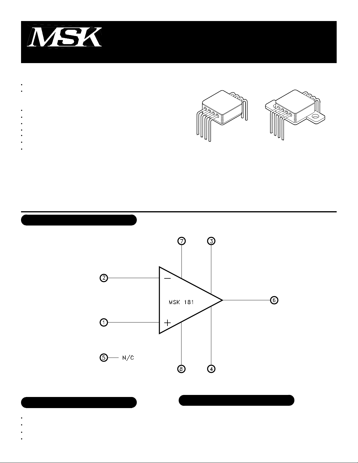
current out DAC. The MSK 181 is packaged in a hermetically sealed 8 pin power dip and the MSK 181Z is offered with bolt down
tabs for applications that require heat sinking.
EQUIVALENT SCHEMATIC
TYPICAL APPLICATIONS
Servo Driver
Actuator Driver
Audio Amplifier
Power Supplies
PIN-OUT INFORMATION
+VIN
1
-VIN
2
ILIM
3
E/S
4
1
8
7
6
5
-Vcc
+Vcc
Output
N/C
PRELIMINARY Rev. C 8/01
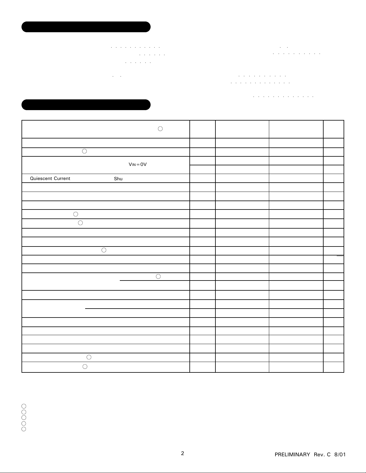
ABSOLUTE MAXIMUM RATINGS
VCC
±IOUT
VIND
VIN
TJ
Total Supply Voltage
Output Current (within S.O.A.)
Input Voltage (Differential)
Input Voltage (Common Mode)
Junction Temperature
ELECTRICAL SPECIFICATIONS
Parameter
STATIC
Supply Voltage Range
Quiescent Current
Quiescent Current
INPUT
Input Offset Voltage
Input Offset Voltage Drift
Input Bias Current
Input Offset Current
Input Impedance
Input Capacitance
Common Mode Rejection Ratio
Input Voltage Noise Density
OUTPUT
Output Voltage Swing
Output Current
Shutdown Input Mode
Output Disable Time
Output Enable Time
TRANSFER CHARACTERISTICS
Slew Rate
Open Loop Voltage Gain
Settling Time ±0.1%
2
2
2
2
(-VCC)-0.1≤ VIN ≤ (+VCC)-3V
VES High- Output Enabled E/S Open or High
VES Low- Output Disabled E/S Forced Low
AV=1 VOUT= 50Vp-p RL=8Ω
2
2
○○○○○○○○○○○
○○○○○○
○○○○○○
60V
5A
±29.5V
+27V/-29V
○○
Internal Protection
(See Application Note)
Test Conditions
VIN=0V
Shutdown Mode VIN=0V
VIN=0V
VIN=0V
VIN=0V
VIN=OV
f=DC
f=DC
f=1KHZ
IOUT=0.6A
IOUT=3.0A
DC=Continuous
VOUT=±25V RL=1KΩ
AV=10 50V Step
1
2
TST
Storage Temperature Range
TLD
Lead Temperature Range
(10 seconds)
TC
Case Operating Temperature
(MSK181H/E)
(MSK181)
RTH
Thermal Resistance
○○○○○○○○○○
○○○○○○○○○○○○○
Junction to Case
Min.
±4
-
-
-
-
-
-
±1
-
-
80
-
±27
±25.5
±3
-27.5
-
-
-
-
90
-
MSK181H/E
Typ.
-
±17
±17
±6
±2
±30
±100
±5
7
10
6
95
90
±28
±26
-
-
-
1
3
10
98
15
Group A
Subgroup
-
1
2,3
-
1
-
1
1
-
-
1
-
4
4
4
4
4
-
-
-
4
-
-65°C to +150°C
○○
○○○○○○○○○○
-55°C to +125°C
-40°C to +85°C
○○○○○○○○○○○○○
MSK181
Typ.
Max.
±30
±20
±20
-
±10
-
±500
±50
-
-
-
-
-
-
-
-
-29
-
-
-
-
-
Min.
±4
-
-
-
-
-
-
-
-
-
75
-
±26
±24
±3
-27.5
-
-
-
-
88
-
±17
±6
±2
±30
±100
±5
±28
±26
10
95
90
98
18
Max.
-
±30
±23
-
±15
±750
±75
7
6
-
-
-
-29
1
3
8
300°C
1.8°C/W
Units
mA
mA
-
mA
-
mV
µV/°C
-
-
-
-
nV/√HZ
-
-
-
-
-
-
-
V/µS
-
-
-
V
nA
nA
Ω
pF
dB
V
V
A
V
V
µS
µS
dB
µS
NOTES:
Unless otherwise specified ±VCC= ±30VDC and E/S pin is open.
1
Devices shall be capable of meeting the parameter, but need not to be tested. Typical parameters are for reference only.
2
Industrial grade and 'E' suffix devices shall be tested to subgroups 1 and 4 unless otherwise specified.
3
Military grade devices ('H' suffix) shall be 100% tested to subgroups 1,2,3 and 4.
4
Subgroup 1,4 TA=TC=+25°C
5
Subgroup 2 TA=TC=+125°C
Subgroup 3 TA=TC=-55°C
2
PRELIMINARY Rev. C 8/01
 Loading...