

MSK MSK173B, MSK173B-1, MSK173-1, MSK173 Datasheet
Half and Full Bridge Motor Drives
Audio Power Amplifiers
Headphones
Cellular Phones, PCMCIA, PDA
Ideal for Single Supply Systems
5V - Peripheral
12V - Automotive
28V - Avionic
4707 Dey Road Liverpool, N.Y. 13088 (315) 701-6751
FEATURES:
ISO-9001 CERTIFIED BY DSCC
M.S.KENNEDY CORP.
Extremely Compact Surface Mount Package
Low Cost Dual High Power Amplifier
Wide Supply Voltage Range: 5V to 40V
High Output Current: 2A
High Efficiency: |Vs-2.2V| at 2A
Internal Current Limit
Wide Common Mode Range
(Includes Negative Supply Voltage)
Low Distortion
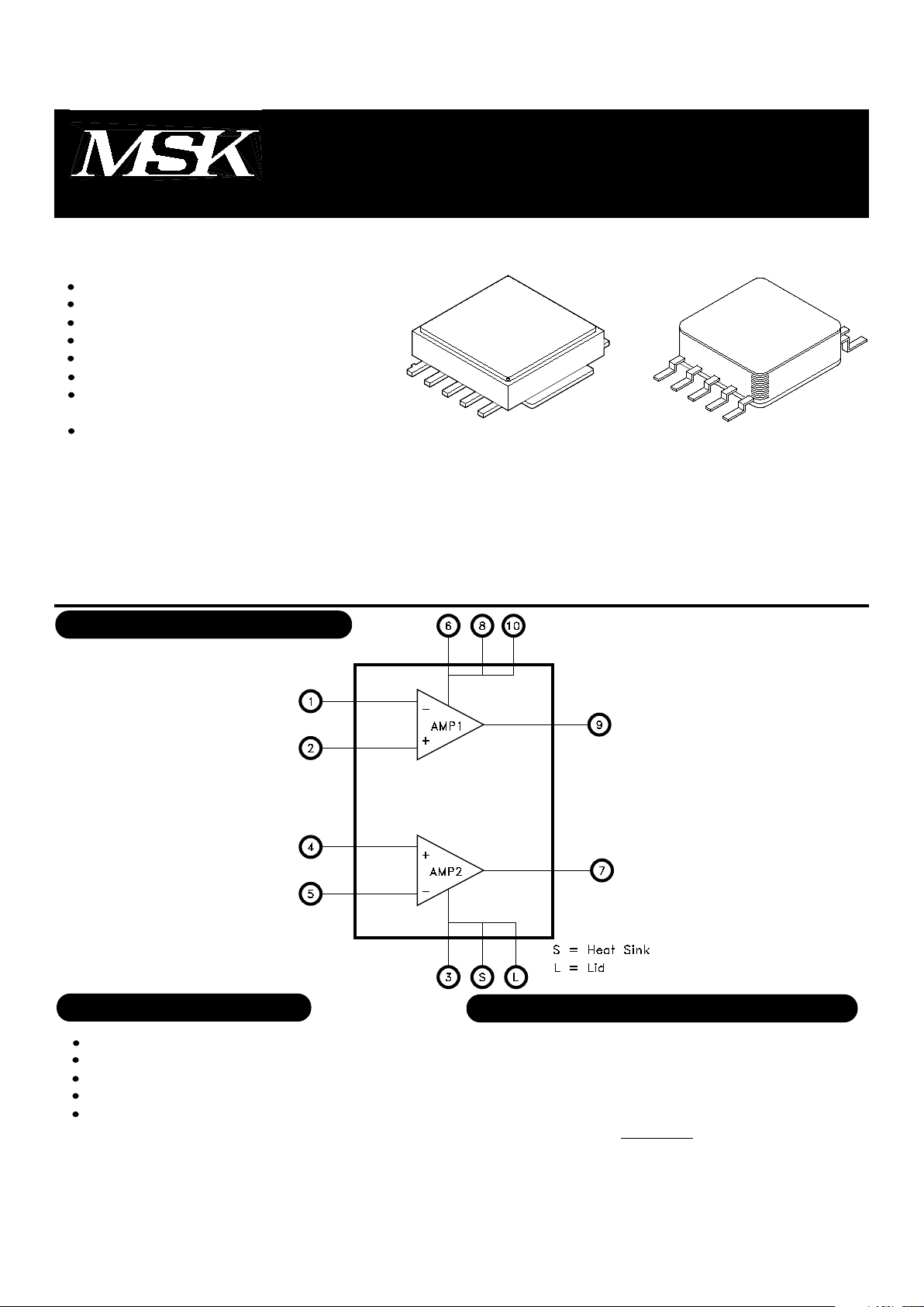
EQUIVALENT SCHEMATIC
The MSK 173 is a high power dual operational amplifier. Each amplifier is capable of delivering two amps of
current to the load. The MSK 173 is an excellent low cost alternative for bridge mode configurations since both
amplifiers are packaged together and will track thermally. The wide common mode range includes the negative rail,
facilitating single supply applications. It is possible to have a "ground based" input driving a single supply amplifier
with ground acting as the second or "bottom" supply of the amplifier. The output stage is current limit protected to
approximately 4.0 amps. The MSK 173 is packaged in an extremely space efficient 10 pin power SOIC package. The
MSK 173-1 is packaged in a 10 pin flatpack. Consult the factory for other packaging options if desired.
DESCRIPTION:
1
All power pins must be
electrically connected
for proper operation.
PIN-OUT INFORMATION
1
2
3
4
5
-Input 1
+Input 1
-Vcc
+Input 2
-Input 2
+Vcc
Output 1
+Vcc
Output 2
+Vcc
Rev. H 8/00
The heat sink of the package and the lid are electrically
connected to -Vcc. The heat sink tab must be connected
to the system -Vcc.
HEAT SINK
10
9
8
7
6
TYPICAL APPLICATIONS
173/173-1
HIGH POWER DUAL
OPERATIONAL AMPLIFIER
MSK173
MSK173-1
MIL-PRF-38534
1
2
3
4
5
6
STATIC
Supply Voltage Range
INPUT
Offset Voltage Drift
Power Supply Rejection
Common Mode Rejection
Total Noise
OUTPUT
Output Voltage Swing
Output Current Peak
Current Limit
Power Bandwidth
Crosstalk
Capacitive Load
TRANSFER CHARACTERISTICS
Slew Rate
Open Loop Voltage Gain
(Split Supply)
Total; VIN=0V
VIN=0V
VCM=0V
Full Temp.
∆VCC=±15V
VCM=±10VDC
RL=500Ω AV=1 CL=1500pF
VOUT=MAX
VOUT=28VPP
IOUT=1A f=1KHz
AV=+1V/V
F=10Hz RL=500Ω
-65°C to +150°C
300°C
-55°C to+125°C
-40°C to +85°C
3.0°C/W
12.0°C/W
Storage Temperature
Lead Temperature
Case Operating Temperature
(MSK173B,173B-1 )
(MSK173,173-1)
Thermal Resistance (DC)
Junction to Case
MSK 173
MSK 173-1
Total Supply Voltage
Output Current (within S.O.A.)
Input Voltage (Differential)
Input Voltage
(Common Mode)
Junction Temperature
40V
3A PK
±VCC
+VCC, -VCC-0.5V
150°C
ABSOLUTE MAXIMUM RATINGS
TST
TLD
TC
RTH
○○○○○○○○○○○○○
VCC
±IOUT
VIND
VIN
TJ
Unless otherwise noted ±VCC=±15VDC.
Devices shall be capable of meeting the parameter, but need not be tested. Typical parameters are for reference only.
Industrial grade devices shall be tested to subgroups 1 and 4 unless otherwise requested.
Military grade devices ('B' suffix) shall be 100% tested to subgroups 1,2,3 and 4. Consult factory for availability of military grade devices.
Subgroup 5 and 6 testing available upon request.
Subgroup 1,4 TC=+25°C
Subgroup 2,5 TC=+125°C
Subgroup 3,6 TA=-55°C
○○○○○○○○○○○○
○○○○
○○○○
○○○○○○○○
○○○○○
Group A
Subgroup
-
1
2
3
1
2, 3
-
-
-
-
-
-
4
-
-
-
-
-
4
-
Typ.
±15
±35
±50
±30
±0.5
±2.0
±20
±35
±75
80
85
0.1
±14.2
±3.0
±4.0
13.6
68
0.22
1.2
100
Min.
±2.5
-
-
-
-
-
-
-
-
60
60
-
±14
±2.0
-
-
60
-
0.5
80
Min.
±2.5
-
-
-
-
-
-
-
-
60
60
-
±14
±2.0
-
-
-
-
0.5
80
Max.
±20
±60
-
-
±15
-
-
±1000
-
-
-
1.0
-
-
-
-
-
-
-
-
Typ.
±15
±35
-
-
±2
-
±20
±35
±75
80
85
0.1
±14.2
±3.0
±4.0
13.6
68
0.22
1.2
100
Units
V
mA
mA
mA
mV
mV
µV/°C
nA
nA
dB
dB
mV
V
A
A
KHz
dB
µF
V/µS
dB
Parameter
Max.
±20
±50
±75
±50
±10
±15
±50
±500
±1000
-
-
1.0
-
-
-
-
-
-
-
-
Test Conditions
ELECTRICAL SPECIFICATIONS
NOTES:
Quiescent Current
○○○○○○○
○○○○○○○○○
○○○○○○○
VIN=0VOffset Voltage
Input Bias Current
2
4
○○○○○○○○○○○○○○○○○
○○○○○○○○○○○○○○○
4
MSK173
MSK173-1
2
2
2
2
2
2
2
2
2
1
2
MSK173B
MSK173B-1
Rev. H 8/00
 Loading...