

MSK MSK165, MSK165B Datasheet
ISO-9001 CERTIFIED BY DSCC
ULTRA HIGH VOLTAGE DUAL
OPERATIONAL AMPLIFIER
165
M.S.KENNEDY CORP.
4707 Dey Road Liverpool, N.Y. 13088 (315) 701-6751
FEATURES:
Internally Compensated For Gains > 10 V/V
Monolithic MOS Technology
High Voltage Operation : 350V
Low Quiescent Current : 4mA Total
High Output Current : 60mA Min. Per Channel
No Second Breakdown
High Speed : 40V/µS Typ.
Space Efficient Dual Amplifier
MIL-PRF-38534 QUALIFIED
MSK165
DESCRIPTION:
The MSK 165 is an ultra high voltage dual monolithic MOSFET operational amplifier ideally suited for electrostatic
transducer and electrostatic deflection applications. With a total supply voltage rating of 350 volts and 60mA of
output current available from each amplifier, the MSK 165 is also an excellent low cost choice for high voltage piezo
drive circuits. The MOSFET output frees the MSK 165 from secondary breakdown limitations and power dissipation
is kept to a minimum with a quiescent current rating of only 4mA total. The MSK 165 is internally compensated for
gains of 10 V/V or greater and is packaged in a hermetically sealed 14 pin power dip with heat sink bolt down tabs.
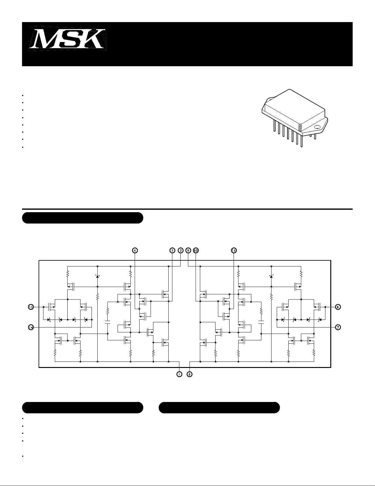
EQUIVALENT SCHEMATIC
TYPICAL APPLICATIONS
High Voltage Piezo Electric Positioning
Electrostatic Deflection
Computer to Vacuum Tube Interface
Ultra High Voltage
Dual Op-Amp Applications
Bridge Amplifier
PIN-OUT INFORMATION
-Vcc 1
1
+Vcc 1
2
Output Drive 1
3
Current Sense 1
4
N/C
5
Inverting Input 2
6
Non -Inverting Input 2
7
1
Non-Inverting Input 1
14
Inverting Input 1
13
N/C
12
Current Sense 2
11
Output Drive 2
10
+Vcc 2
9
-Vcc 2
8
Rev. A 8/00
ABSOLUTE MAXIMUM RATINGS
2
VCC
±IOUT
±IOUTP
VIND
VIN
TJ
Total Supply Voltage
Output Current (within S.O.A.)
Output Current Peak
Input Voltage (Differential)
Input Voltage (Common Mode)
Junction Temperature
○○○○○○○○○○○
○○○○○○○○○○
○○○○○○○
○○○○○○○○○
ELECTRICAL SPECIFICATIONS
○○○○○
120mA
○○○○
350V
60mA
±16V
±Vcc
150°C
Storage Temperature
TST
Lead Temperature
TLD
Case Operating Temperature
TC
(MSK165B)
(MSK165)
Thermal Resistance (DC Each Amplifier)
RTH
○○○○○○○○○○○
○○○○○○○○○○○○○
Junction to Case
○○○○○
○○○○○○○○○○○○○○
○○○○○○○○○○○○○○
-65°C to +150°C
300°C
-55°C to +125°C
-40°C to +85°C
12°C/W
Parameter
STATIC
Supply Voltage Range
2
Quiescent Current
INPUT
Offset Voltage
Offset Voltage Drift
Offset Voltage vs ±Vcc
Input Bias Current
Input Impedance
Input Capacitance
4
4
4
4
4
Common Mode Rejection
Noise
OUTPUT
Output Voltage Swing
Output Current
Power Bandwidth
Resistance
Settling Time to 0.1%
Capacitive Load
4
4
3
4
TRANSFER CHARACTERISTICS
Slew Rate
Open Loop Voltage Gain
4
Min.
±50
-
-
-
-
-
-
-
-
-
-
84
-
±138
±60
-
-
-
10
20
94
MSK165B
Typ.
±150
±1.4
±2.0
±1.0
±15
±40
±20
±5
-
11
10
5
94
50
±141
±120
26
150
12
-
40
106
Max.
±175
±2.0
±3.0
±2.1
±30
±65
±32
±50
±50
-
-
-
-
-
-
-
-
-
-
-
-
Test Conditions
1
Group A
Subgroup
4
9
-
1
VIN=0V
2
3
VIN=0V
VIN=0V
VIN=0V
VCM=0V
1
2,3
1
1,3
2
(DC)
-
-
4
VCM=±90VDC
1Hz≤f≤10Hz
IOUT=±40mA Peak
VOUT=MAX
VOUT=280VPP
No Load RCL=0Ω
4
10V Step
AV=+1V/V
-
-
4
4
-
-
-
-
4
F=15Hz RL=5KΩ
4
Min.
±50
-
-
-
-
-
-
-
-
-
-
84
-
±138
±60
-
-
-
10
10
94
MSK165
Typ.
±150
±1.4
-
-
±15
±40
±20
±5
-
11
10
5
94
50
±141
±120
26
150
12
-
20
106
Max.
±175
±2.0
-
-
±30
-
±32
±100
-
-
-
-
-
-
-
-
-
-
-
-
-
Units
V
mA
mA
mA
mV
µV/°C
µV/V
pA
nA
Ω
pF
dB
µVRMS
V
mA
KHz
Ω
µS
nF
V/µS
dB
NOTES:
1
Unless otherwise noted, ±VCC= ±150VDC and specifications apply to each amplifier.
2
Derate maximum supply voltage 0.5V/°C below TC=+25°C. No derating is needed above TC=25°C.
3
AV=-10V/V measured in false summing junction circuit.
4
Devices shall be capable of meeting the parameter, but need not be tested. Typical parameters are for reference only.
5
Industrial grade devices shall be tested to subgroups 1 and 4 unless otherwise requested.
6
Military grade devices ('B' suffix) shall be 100% tested to subgroups 1,2,3 and 4.
7
Subgroup 5 and 6 testing available upon request.
8
Subgroup 1,4 TC=+25°C
Subgroup 2,5 TC=+125°C
Subgroup 3,6 TA=-55°C
9
Electrical specifications are derated for power supply voltages less than ±50VDC.
Rev. A 8/002
 Loading...