

MSK MSK155, MSK155E, MSK155H Datasheet
ISO-9001 CERTIFIED BY DSCC
HIGH POWER DUAL
OPERATIONAL AMPLIFIER
155
M.S.KENNEDY CORP.
4707 Dey Road Liverpool, N.Y. 13088 (315) 701-6751
FEATURES:
Available to DSCC SMD #5962-02509HX
Space Efficient Dual Power Amplifier
Low Cost
High Voltage Operation: Up to 80V
Low Quiescent Current: 40mA Typ. Total
High Output Current: 5A Min. Per Amp
High Speed: 10V/µS Typ.
Monolithic Technology
Replaces obsolete MSK 154 up to 80V
MIL-PRF-38534 QUALIFIED
DESCRIPTION:
The MSK 155 is a high power dual monolithic operational amplifier ideally suited for high power amplification and
magnetic deflection applications. With a total supply voltage rating of 80 volts and 5A of available output current per
amplifier, the MSK 155 is also an excellent low cost choice for motor drive circuits. With both amplifiers in the same
package, thermally induced output offset voltages are eliminated. Power dissipation is kept to a minimum with a total
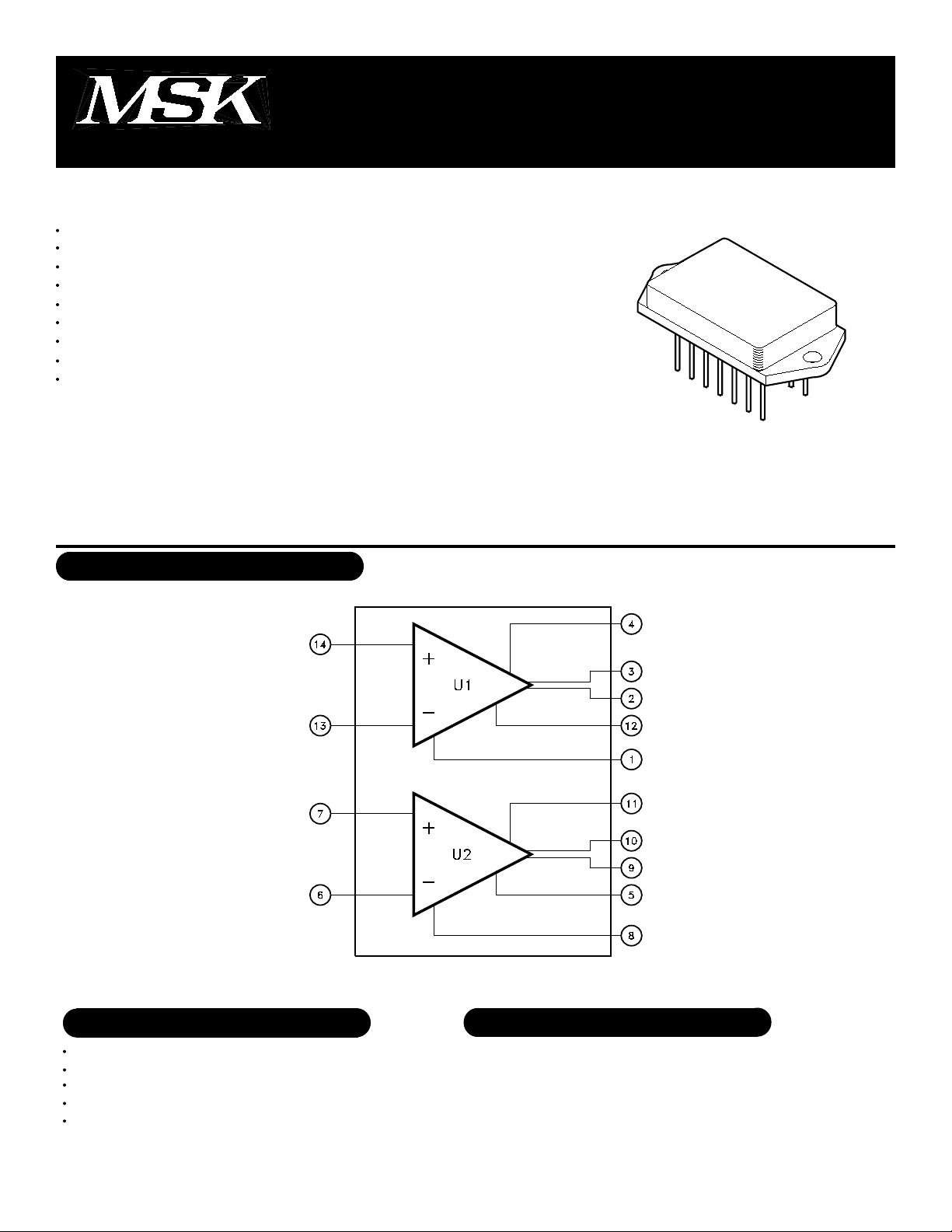
quiescent current rating of only 40mA. The MSK 155 is packaged in a hermetically sealed 14 pin power dip with heat
sink bolt down tabs.
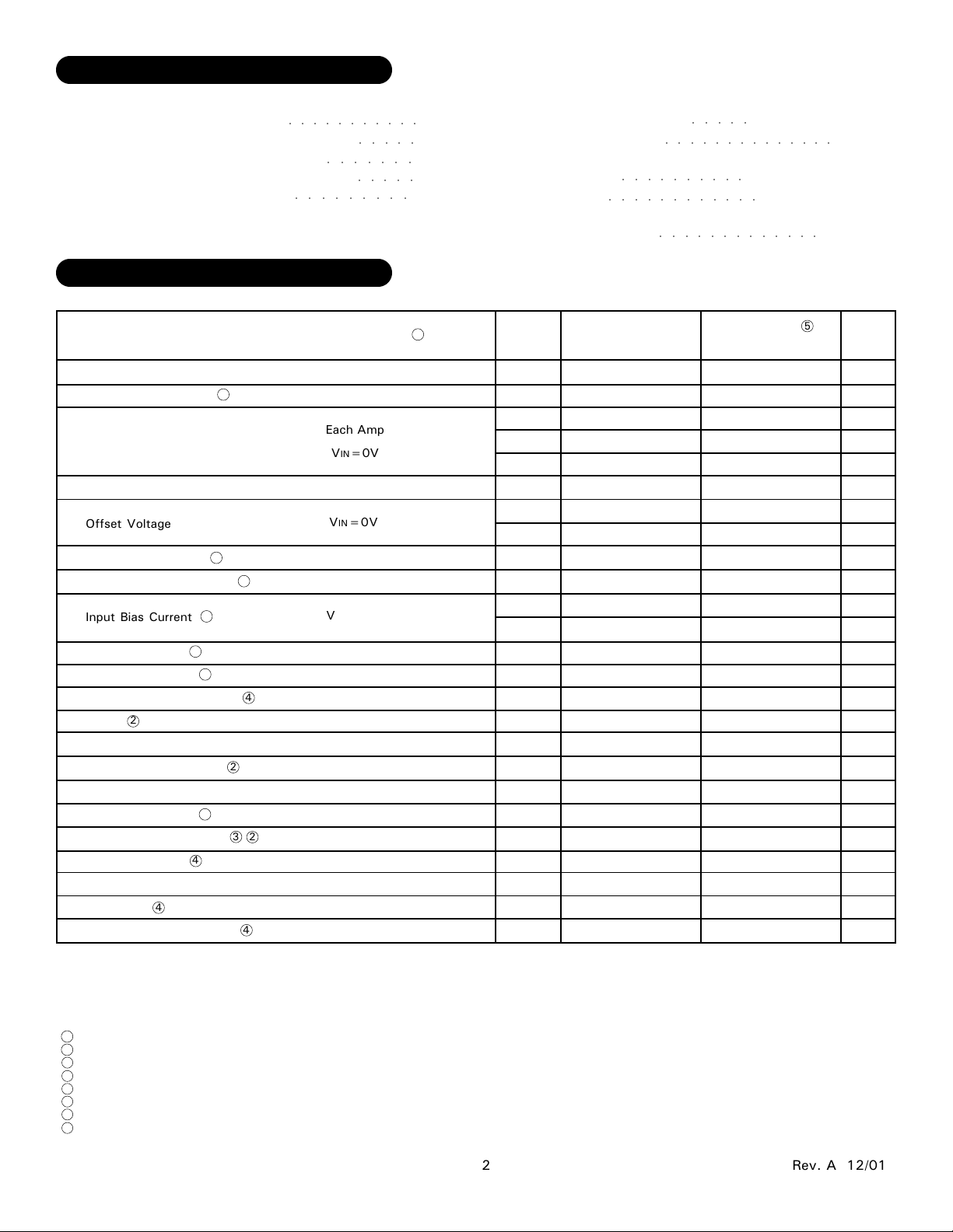
EQUIVALENT SCHEMATIC
TYPICAL APPLICATIONS
PA Audio
Magnetic Deflection
Motor Drive
Noise Cancellation
High Power Bridge Amplifier
PIN-OUT INFORMATION
1
-Vcc1
2
Output Drive 1B
3
Output Drive 1A
4
+Vcc1
5
Current Sense 2
6
Inverting Input 2
7
Non Inverting Input 2
1
14
Non Inverting Input 1
13
Inverting Input 1
12
Current Sense1
11
+Vcc 2
10
Output Drive 2A
9
Output Drive 2B
8
-Vcc 2
Rev. A 12/01
ABSOLUTE MAXIMUM RATINGS
VCC
±IOUT
VIND
VIN
TJ
Total Supply Voltage
Output Current (within S.O.A.)
Input Voltage (Differential)
Input Voltage (Common Mode)
Junction Temperature
ELECTRICAL SPECIFICATIONS
Parameter
STATIC
Supply Voltage Range
Quiescent Current
INPUT
Offset Voltage
Offset Voltage Drift
Offset Voltage vs ±Vcc
Input Bias Current
Input Impedance
Input Capacitance
Common Mode Rejection
Noise
2
OUTPUT
Output Voltage Swing
Output Voltage Swing
Power Bandwidth
Settling Time to 0.1%
Capacitive Load
TRANSFER CHARACTERISTICS
Slew Rate
4
Open Loop Voltage Gain
4
4
2
4
2
2
4
2
4
4
RL = 10Ω VOUT=20VRMS
2
3
VOUT = ±10V RL = 10Ω
4
○○○○○○○○○○○
○○○○○
○○○○○○○
○○○○○
○○○○○○○○○
150°C
Test Conditions
Each Amp
VIN=0V
VIN=0V
VIN=0V
VIN=0V
VCM=0V
(DC)
VCM=±22VDC
F = 10Hz to 1KHz
RL=10K
IOUT=5A Pk
2V Step
AV=+10V/V
F=10Hz RL = 10KΩ
80V
±5A
±Vcc
±Vcc
1
TST
Storage Temperature
TLD
Lead Temperature
TC
Case Operating Temperature
(MSK155H/E)
(MSK155)
RTH
Thermal Resistance (DC)
○○○○○○○○○○
○○○○○○○○○○○○
Junction to Case
Group A
Subgroup
-
1
2
3
1
2,3
2,3
-
1
2, 3
-
-
4
-
-
4
4
-
-
4
4
MSK155H/E
Min.
±10
-
-
-
-
-
-
-
-
-
-
-
95
-
-
±29
45
-
10
6
95
Typ.
±35
±20
±20
±20
±0.1
±2
±10
±5
±20
-
10
5
110
10
±33.5
±30
55
2
-
10
100
○○○○○
○○○○○○○○○○○○○○
-65°C to +150°C
-55°C to +125°C
-40°C to +85°C
○○○○○○○○○○○○○
MSK155
90
40
10
90
Typ.
±35
±20
-
-
-
-
-
-
-
-
-
-
-
-
-
±0.1
-
±10
±5
±20
-
10
5
110
10
-
±33.5
-
±30
55
-
2
-
10
6
100
12
Max.
±40
±30
±30
±30
±2
±10
±50
-
±100
±10
-
-
-
-
-
-
-
-
-
-
-
Min.
±10
±29
12
2.0°C/W
5
Max.
±40
±35
-
-
±10
-
-
-
±200
-
-
-
-
-
-
-
-
-
-
-
-
300°C
Units
V
mA
mA
mA
mV
mV
µV/°C
µV/V
pA
nA
Ω
pF
dB
µVRMS
V
V
KHz
µS
nF
V/µS
dB
NOTES:
1
Unless otherwise noted ±VCC= ±35VDC, RCL = 0Ω and specifications apply to each amplifier.
2
Typical parameters are for reference only.
3
AV=-1V/V measured in false summing junction circuit.
4
Devices shall be capable of meeting the parameter, but need not be tested.
5
Industrial grade and 'E' suffix devices shall be tested to subgroups 1 and 4 unless otherwise requested.
6
Military grade devices ('H' suffix) shall be 100% tested to subgroups 1,2,3 and 4.
7
Subgroup 5 and 6 testing available upon request.
8
Subgroup 1,4 TC=+25°C
Subgroup 2,5 TC=+125°C
Subgroup 3,6 TA=-55°C
2
Rev. A 12/01
 Loading...