

MSK MSK1461B, MSK1461 Datasheet
ISO 9001 CERTIFIED BY DSCC
HIGH SPEED/VOLTAGE
OP AMP
1461
M.S.KENNEDY CORP.
4707 Dey Road Liverpool, N.Y. 13088 (315) 701-6751
FEATURES:
Extremely Fast - 500v/µS
Wide Supply Range ±15V to ±45V
VMOS Output, No S.O.A. Restrictions
Large Gain-Bandwidth Product
FET Input
Electrically Isolated Case
800mA Typical Output Current
MIL-PRF-38534 CERTIFIED
DESCRIPTION:
The MSK 1461 is a state of the art high speed FET input operational amplifier. The distinguishing characteristic
of the MSK 1461 is its unique VMOS output stage which completely eliminates the safe operating area restrictions
associated with secondary breakdown of bipolar transistor output stage op-amps. Freedom from secondary break-
down allows the 1461 to handle large output currents at any voltage level limited only by transistor junction tempera-
ture. 115 dB of open loop gain gives the 1461 high closed loop gain accuracy and the typical ±1.0mV of input offset
voltage will fit well in any error budget. A 500 V/µS slew rate and 1200 MHz gain bandwidth product make the 1461
an outstanding high-speed op-amp. A single external capacitor is used for compensation and output current limiting
is user programmable through the selection of two external resistors.
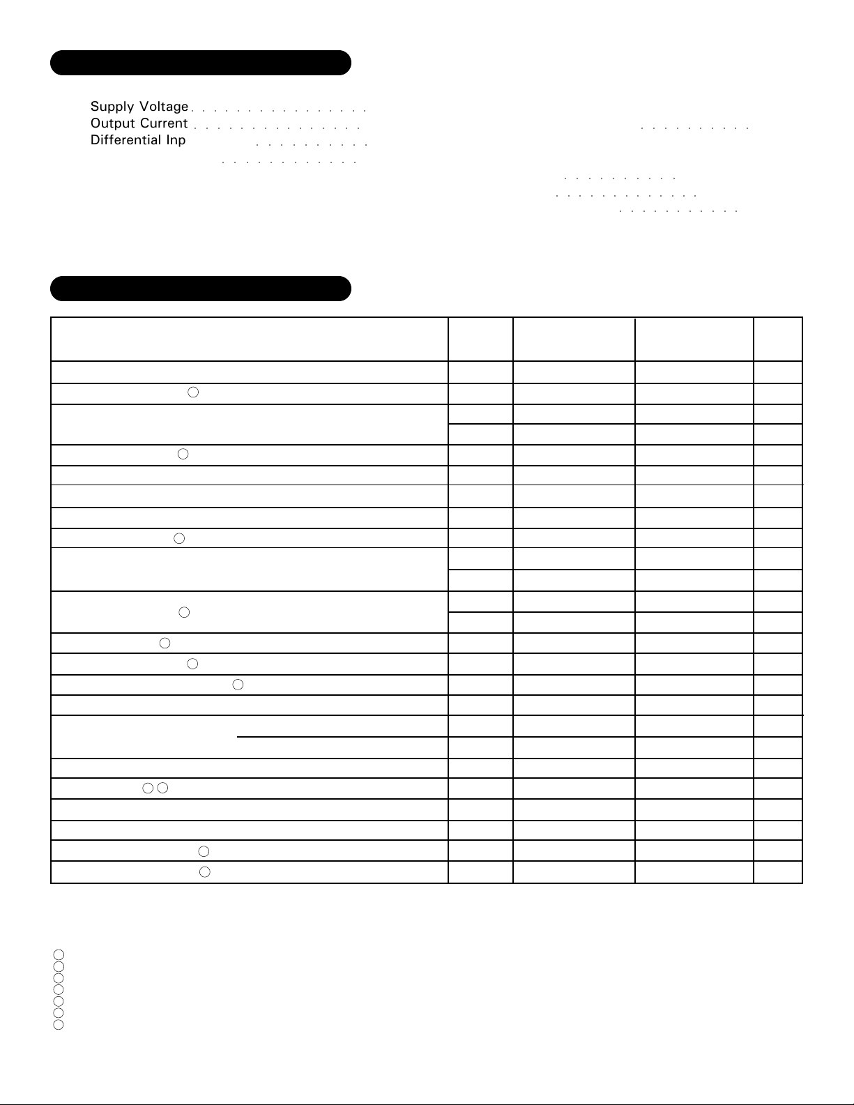
EQUIVALENT SCHEMATIC
TYPICAL APPLICATIONS
PIN-OUT INFORMATION
Video Yoke Drivers
Video Distribution Amplifiers
High Accuracy Audio Amplification
High Speed ATE Pin Drivers
Inverting Input
1
Non-Inverting Input
2
No Connection
3
No Connection
4
Negative Power Supply
5
Negative Current Limit
6
No Connection
7
1
8
Output
9
Positive Current Limit
10
Positive Power Supply
11
Compensation
12
Compensation
13
Offset Adjust
14
Offset Adjust
Rev. B 8/00
ABSOLUTE MAXIMUM RATINGS
±VCC
Supply Voltage
IOUT
Output Current
VIN
Differential Input Voltage
RTH
Thermal Resistance
○○○○○○○○○○○○○○○○
○○○○○○○○○○○○○○○
○○○○○○○○○○○○
Junction to Case
(Output Devices Only)
ELECTRICAL SPECIFICATIONS
Parameter
STATIC
Supply Voltage Range
Quiescent Current
Thermal Resistance
INPUT
Input Offset Voltage
Input Offset Voltage Drift
Input Offset Adjust
Input Bias Current
Input Offset Current
Input Impedance
Common Mode Range
Common Mode Rejection Ratio
OUTPUT
Output Voltage Swing
Output Current, Peak
Settling Time
2
TRANSFER CHARACTERISTICS
Slew Rate
Open Loop Voltage Gain
Gain Bandwidth Product
3
3
3
3
3
3
3
3
VOUT=±10V RL=1KΩ AV=-5V/V
3
3
±45V
800mA
○○○○○○○○○○
±25V
12°C/W
Test Conditions
VIN=0V
Junction to Case
VIN=0V AV=-10V/V
Bal. Pins=N/C
RPOT=10KΩ to +VCC
VCM=0V
Either Input
VCM=0V
F=DC
F=10KHz VCM=±22V
RL=50Ω AV=-5V/V
RL=1KΩ
RL=33Ω AV=-5V/V TJ<175°C
0.1% 10V step
RL=1KΩ F=100Hz
F=100KHz
Storage Temperature Range
TST
Lead Temperature Range
TLD
(10 Seconds)
Case Operating Temperature
TC
(MSK 1461B)
(MSK 1461)
Junction Temperature
TJ
Group A
Subgroup
-
1
2,3
-
1
2,3
-
1
2,3
-
-
-
-
4
4
4
4
4
4
4
4
Min.
±15
±22
±27
±30
±600
200
800
○○○○○○○○○○
○○○○○○○○○○○○○
Typ.
-
±19
-
±21
-
11
-
±1.0
-
±6.0
-
±8.0
-
±10
-
±10
-
±5.0
-
±5.0
-
3x10
-
±24
100
90
±31
±33
±800
400
-
500
106
90
1200
-65°C to +150°C
○○○○○○○○○○
-55°C to +125°C
○○○○○○○○○○○
MSK 1461MSK 1461B
Typ.
12
Min.
±15
±19
-
-
-
±1.0
-
±10
-
±8.0
-
-
±10
-
-
±5.0
-
-
-
-
-
-
-
-
-
-
-
-
-
-
±22
90
±27
±30
±600
-
200
90
800
3x10
±24
100
±31
±33
±800
400
500
106
1200
Max.
±45
±25
±35
±5.0
±50
±300
±100
800
300°C
-40°C to 85°C
+175°C
Max.
-
±45
±28
-
-
11
15
±8.0
-
µV/°C
-
±300
-
-
-
-
-
1212
-
-
-
-
-
-
800
-
-
-
Units
V
mA
mA
°C/W
mV
V
pA
nA
pA
nA
Ω
V
dB
V
V
mA
nS
V/µS
dB
MHz
NOTES:
1
RSC=0Ω and ±VCC=36VDC unless otherwise specified.
2
AV=-1, measured in false summing junction circuit.
3
Devices shall be capable of meeting the parameter, but need not be tested. Typical parameters are for reference only.
4
Industrial grade devices shall be tested to subgroups 1 and 4 unless otherwise specified.
5
Military grade devices ("B" suffix) shall be 100% tested to subgroups 1,2,3 and 4.
6
Subgroups 5 and 6 testing available upon request.
7
Subgroup 1,4
Subgroup 2,5
Subgroup 3,6
TC=+25°C
TJ=+125°C
TA=-55°C
Rev. B 8/002
 Loading...