

MSK MSK130 Datasheet
M.S.KENNEDY CORP.
ISO-9001 CERTIFIED BY DESC
ULTRA HIGH VOLTAGE
HIGH SPEED
DIFFERENTIAL OP-AMP
130
4707 Dey Road Liverpool, N.Y. 13088
(315) 701-6751
FEATURES:
Wide Supply Voltage Range 15V to 400V
Fast Slew Rate - 300 V/µS Typ.
FET Input - Accurate DC Specifications
Electrically Isolated Case
Low Cost Innovative Packaging
Very Low Quiescent Current - 6mA Typ.
Output Current to ±200mA
Adjustable Current Limit
DESCRIPTION:
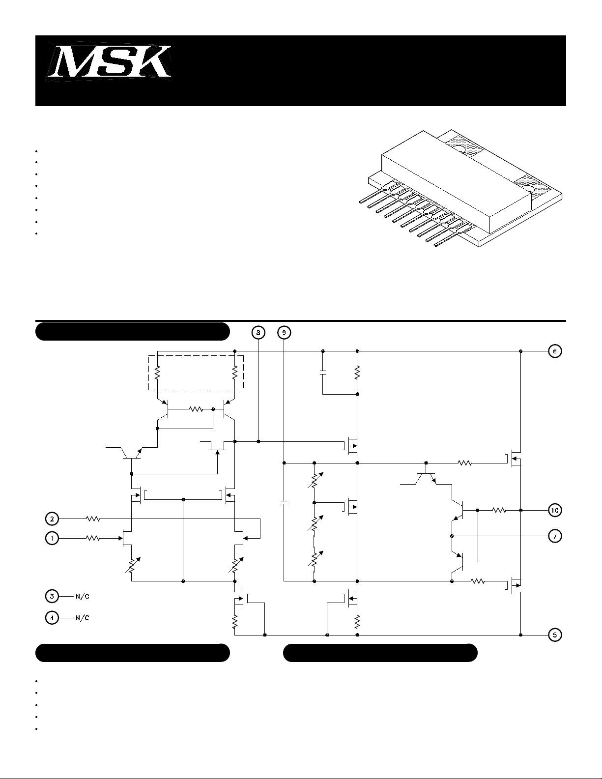
The MSK 130 is a high speed, high voltage differential amplifier designed for output currents up to ±200mA.
Since the MSK 130 utilizes external compensation, it exhibits wide bandwidth and greater stability over a wide gain
range. High frequency, high voltage instrumentation circuits and electrostatic transducers are just a sample of the
applications that the MSK 130 is well suited for. The device is packaged in a 10 pin insulated ceramic SIP with holes
for direct heat sink attachment.
EQUIVALENT SCHEMATIC
TYPICAL APPLICATIONS
Ultra-High Voltage Supplies
FET Input Instrumentation Amplifiers
Electrostatic Deflection
Electrostatic Transducers
Piezo Transducer Excitation
1
-Input
2
+Input
3
No Connection
4
No Connection
5
-Vcc
1
PIN-OUT INFORMATION
10
9
8
7
6
Output
Comp2
Comp1
Isense
+Vcc
Rev. B 7/00
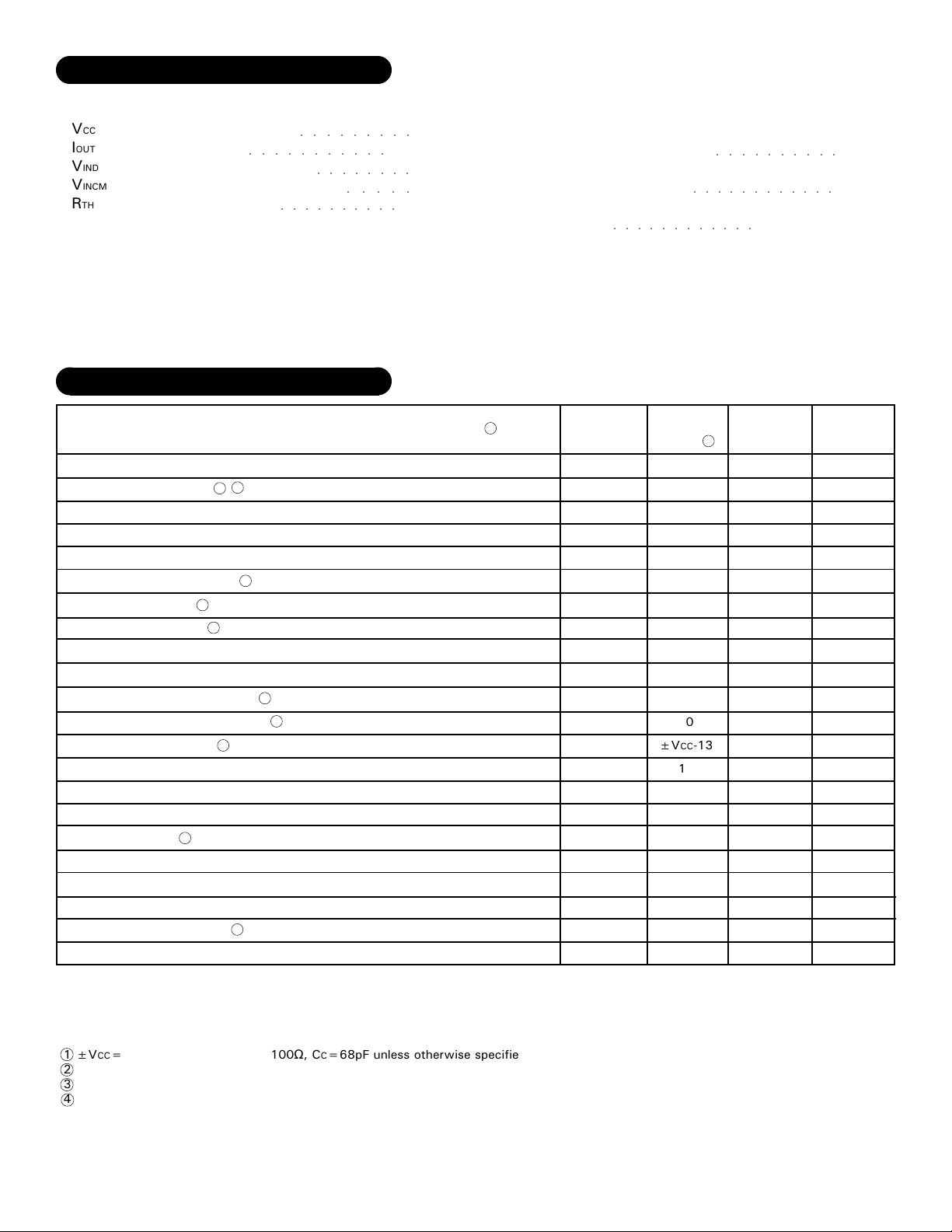
ABSOLUTE MAXIMUM RATINGS
VCC
IOUT
VIND
VINCM
RTH
Supply Voltage (Total)
Output Current
○○○○○○○○○○○
Differential Input Voltage
Common Mode Input Voltage
Thermal Resistance
○○○○○○○○○○
Junction to Case (Output Devices)
ELECTRICAL SPECIFICATIONS
Parameter
STATIC
4
Supply Voltage Range
Quiescent Current
INPUT
Input Offset Voltage
Input Offset Voltage Drift
Input Bias Current
Input Offset Current
Input Impedance
Input Capacitance
Power Supply Rejection Ratio
Common Mode Rejection Ratio
Common Mode Range
Input Noise Voltage
OUTPUT
Output Voltage Swing
Output Current
Output Resistance
TRANSFER CHARACTERISTICS
Slew Rate Limit
Open Loop Voltage Gain
Settling Time to 0.1%
2
2
2
2
2
2
2
2
2
○○○○○○○○○
400V
±300mA
○○○○○○○○
○○○○○
±25V
±Vcc
15°C/W
Test Conditions
Total +VCC to -VCC
VIN=0V
VIN=0V
VIN=0V
VCM=0V Either Input
VCM=0V
F=DC
Either Input
∆ VCC=±15V
F=DC VCM=±50V
Linear Operation
F=100KHz
IOUT=±50mA
Within SOA
f≤10KHz, No Load
AV=100v/v CC=0pF
F=15Hz CC=0pF
RL=1KΩ 2V step CC=10pF
TST
Storage Temperature Range
TLD
Lead Temperature Range
(10 Seconds)
TJ
Junction Temperature
TC
Case Operating Temperature Range
(MSK130)
1
○○○○○○○○○○○○
MSK 130
Min.
20
-
-
-
-
-
-
-
-
80
±VCC-15
-
±91.5
±200
-
-
95
-
±VCC-13
±250
Typ.
-
±6
±0.5
±10
±10
10
10
4.0
±10
90
1.5
±95
50
300
110
1
-65°C to +150°C
○○○○○○○○○○
○○○○○○○○○○○○
-55°C to +125°C
3
11
Max.
400
±8
±2.0
±50
±200
50
-
-
±20
-
-
-
-
-
-
-
-
-
220°C
150°C
Units
V
mA
mV
µV/°C
pA
pA
Ω
pF
µV/V
dB
V
µVrms
V
mA
Ω
V/µS
dB
µS
NOTES:
1
±VCC=±100V, TC=25°C, RC=100Ω, CC=68pF unless otherwise specified.
2
Devices shall be capable of meeting the parameter, but need not be tested.
3
Typical parameters are representative of actual device performance but are for reference only.
4
Maximum supply voltage should be derated 0.625V/°C below 25°C case temperature.
2
Rev. B 7/00
 Loading...