

MSK MSK101B, MSK101 Datasheet
TYPICAL APPLICATIONS
4707 Dey Road Liverpool, N.Y. 13088 (315) 701-6751
MIL-PRF-38534 QUALIFIED
101
ISO-9001 CERTIFIED BY DSCC
M.S.KENNEDY CORP.
FEATURES:
PA Audio
Magnetic Deflection
Bridge Motor Drive
Noise Cancellation
HIGH POWER DUAL
OPERATIONAL AMPLIFIER
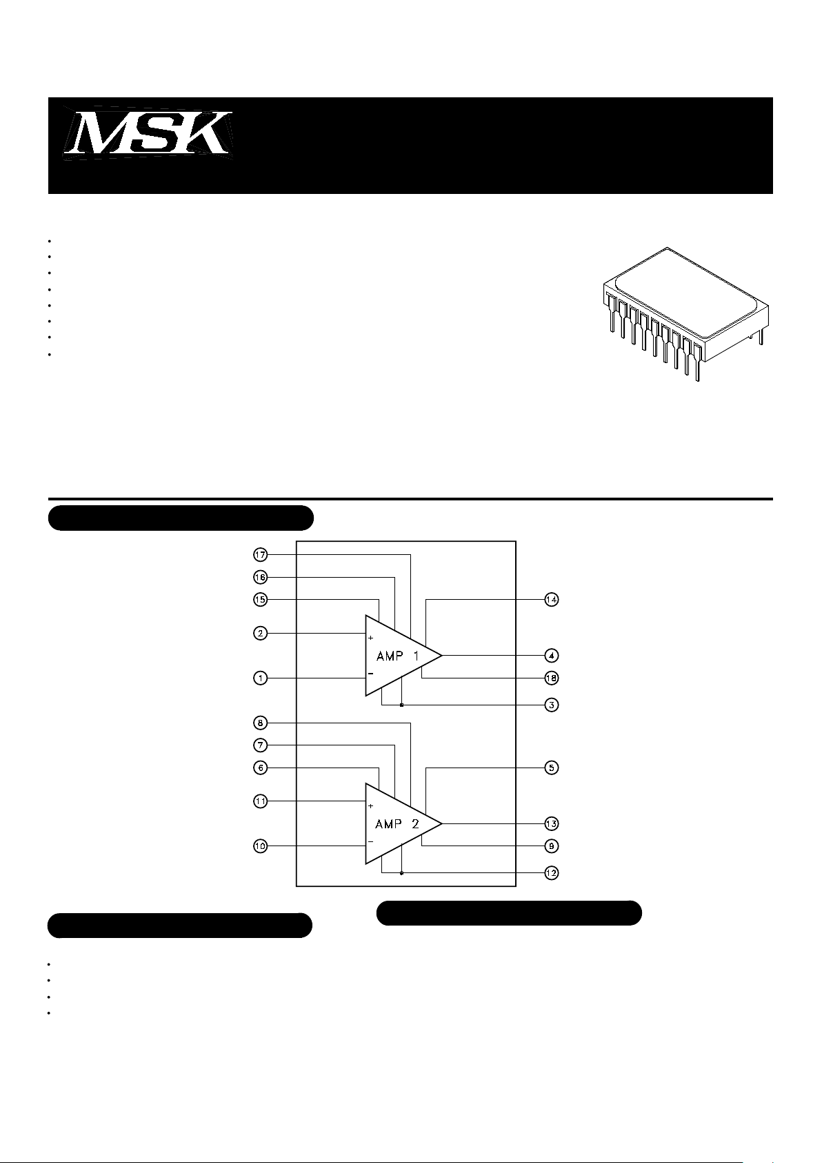
EQUIVALENT SCHEMATIC
TYPICAL APPLICATIONS
DESCRIPTION:
The MSK 101 is a dual high power monolithic MOSFET operational amplifier ideally suited for high power amplifi-
cation and magnetic deflection applications. With a total supply voltage rating of 150 volts and 5A of output current
available from each amplifier, the MSK 101 is also an excellent low cost choice for motor drive circuits. The MOSFET
output frees the MSK 101 from secondary breakdown limitations and power dissipation is kept to a minimum with a
typical quiescent current rating of only ± 8.0 mA total in class "C" mode. Power saving class "C" mode is enabled
by the user externally. The MSK 101 is packaged in a hermetically sealed 18 pin ceramic dip which has two external
compensation pins for each amplifier.
PIN-OUT INFORMATION
Current Sense 1
Amp 1 Comp 2
Amp 1 Comp 1
Quiescent Current Adjust 1
+Vcc 1
Output Drive 2
-Vcc 2
Non-Inverting Input 2
Inverting Input 2
Inverting Input 1
Non-Inverting Input 1
-Vcc 1
Output Drive 1
+Vcc 2
Quiescent Current Adjust 2
Amp 2 Comp 1
Amp 2 Comp 2
Current Sense 2
18
17
16
15
14
13
12
11
10
Operates In Class AB Or Class C Mode
Low Cost
High Voltage Operation : 150V
Low Quiescent Current : ± 8.0 mA Total Typ. In Class "C" Mode
High Output Current : 5A Min. Per Amplifier
No Second Breakdown
High Speed : 27V/µS Typ.
External Compensation For Optimum Gain-Bandwidth
1
2
3
4
5
6
7
8
9
Rev. A 7/00
1
MSK101
STATIC
Supply Voltage Range
Quiescent Current
Quiescent Current (Class 'C')
INPUT
Offset Voltage
Offset Voltage Drift
Offset Voltage vs ±Vcc
Input Impedance
Input Capacitance
Common Mode Rejection
Noise
OUTPUT
Output Voltage Swing
Output Current
Power Bandwidth
Settling Time to 0.1%
Capacitive Load
TRANSFER CHARACTERISTICS
Slew Rate
Open Loop Voltage Gain
Storage Temperature
Lead Temperature
Case Operating Temperature
(MSK101B)
(MSK101)
Thermal Resistance (DC)
Junction to Case
ABSOLUTE MAXIMUM RATINGS
150V
±5A
±16V
±Vcc
150°C
Total Supply Voltage
Output Current (within S.O.A.)
Input Voltage (Differential)
Input Voltage (Common Mode)
Junction Temperature
-65°C to +150°C
300°C
-55°C to +125°C
-40°C to +85°C
5.0°C/W
1
2
3
4
5
6
7
8
TST
TLD
TC
RTH
VCC
±IOUT
VIND
VIN
TJ
Unless otherwise noted CC=10pF, RC=1.0KΩ, ±VCC= ±50VDC and specifications apply to each amplifier.
Derate maximum supply voltage 0.5V/°C below TC=+25°C. No derating is needed above TC=25°C.
AV=-10V/V measured in false summing junction circuit.
Devices shall be capable of meeting the parameter, but need not be tested. Typical parameters are for reference only.
Industrial grade devices shall be tested to subgroups 1 and 4 unless otherwise requested.
Military grade devices ('B' suffix) shall be 100% tested to subgroups 1,2,3 and 4.
Subgroup 5 and 6 testing available upon request.
Subgroup 1,4 TC=+25°C
Subgroup 2,5 TC=+125°C
Subgroup 3,6 TA=-55°C
NOTES:
2
○○○○○○○○○○○
○○○○○
○○○○○
○○○○○○○○○○○○○○
○○○○○○○○○○○
○○○○○○○○○○○○
○○○○○○○○○○○○
○○○○○○○
○○○○○
○○○○○○○○○
Group A
Subgroup
-
1
2
3
1
1
2,3
1
1,3
2
-
-
-
-
4
4
-
-
-
4
4
VIN=0V
VIN=0V
VIN=0V
VIN=0V
VIN=0V
(DC)
VCM=±30VDC
10KHz BW
IOUT=±5A Peak
VOUT=MAX
VOUT=80VPP
10V Step
AV=+1V/V CC=68pF
CC=Open
F=15Hz
Typ.
±50
±30
±20
±35
4
±5
±10
±8
±20
-
10
5
106
10
±42
±5.5
66
2
-
27
106
1
Test Conditions
Max.
±75
±50
±45
±65
6
±10
±50
±15
±100
±50
-
-
-
-
-
-
-
-
-
-
-
Min.
±15
-
-
-
-
-
-
-
-
-
-
-
90
-
±40
±5
-
-
10
20
94
Min.
±15
-
-
-
-
-
-
-
-
-
-
90
-
±40
±5
-
-
10
20
94
Max.
±75
±50
-
-
6
±15
-
±15
±100
-
-
-
-
-
-
-
-
-
-
-
-
Typ.
±50
±30
-
-
4
±5
±10
±8
±20
-
10
5
106
10
±42
±5.5
66
2
-
27
106
Units
V
mA
mA
mA
mA
mV
µV/°C
µV/V
pA
nA
Ω
pF
dB
µVRMS
V
A
KHz
µS
nF
V/µS
dB
MSK101B
MSK101
Parameter
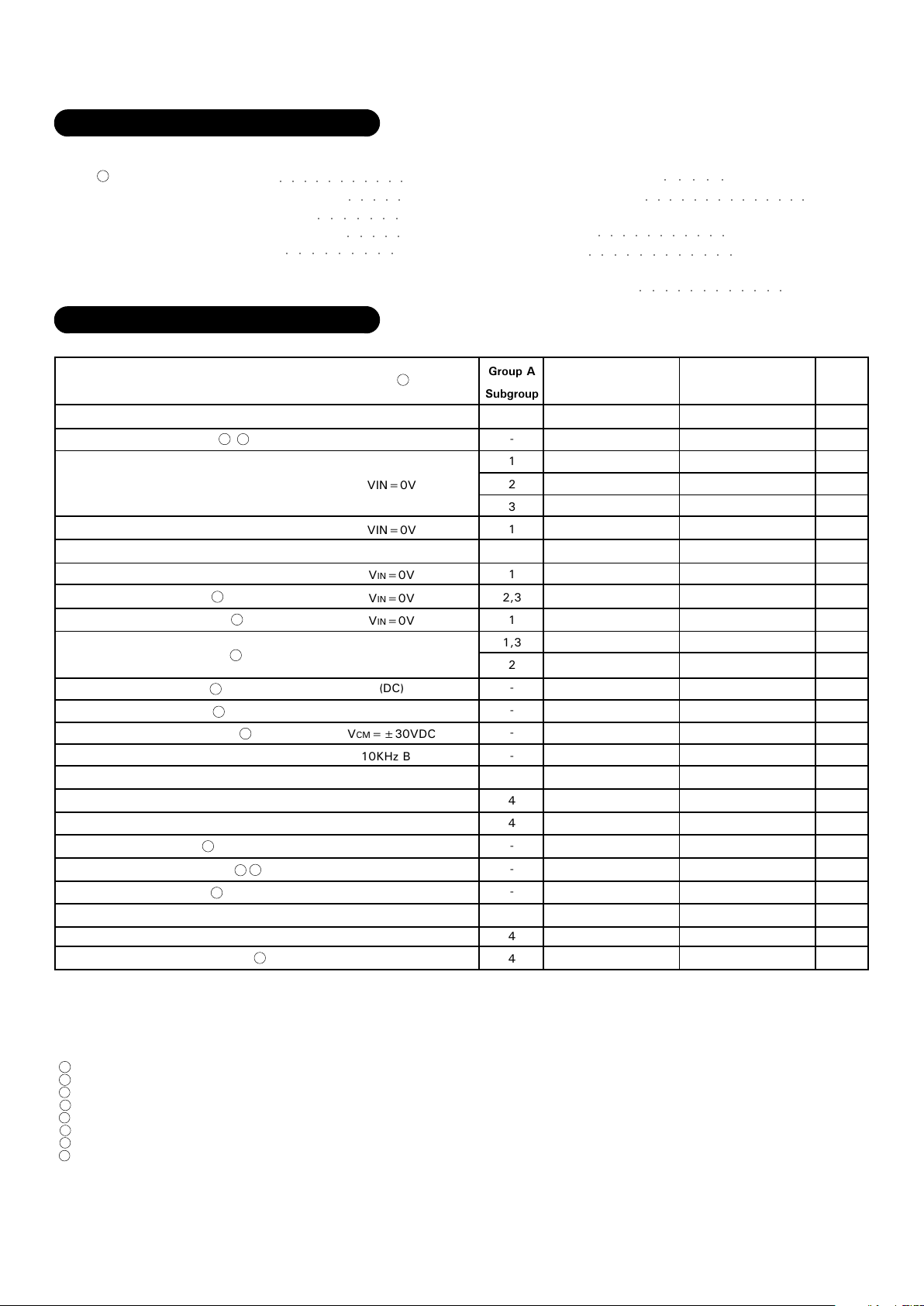
ELECTRICAL SPECIFICATIONS
4
4
3
4
4
4
4
4
4
4
4
2
±±
±
±
11
11
4
Input Bias Current VCM = 0V
2
Rev. A 7/00
 Loading...