

MSK MSK0033B, MSK0033 Datasheet
ISO 9001 CERTIFIED BY DSCC
FET INPUT HIGH SPEED VOLTAGE
FOLLOWER/BUFFER AMPLIFIER
0033
M.S.KENNEDY CORP.
4707 Dey Road Liverpool, N.Y. 13088
FEATURES:
Industry Wide LH0033/EL2005 Replacement
Low Input Offset - 2mV
Low Input Offset Drift - 25µV/°C
FET Input, Low Input Current - 50pA
High Slew Rate - 1500V/µS
Wide Bandwidth - 140MHz
High Output Current - ±100mA
Available to DSCC SMD 5962-80014
MIL-PRF-38534 CERTIFIED
(315) 701-6751
DESCRIPTION:
The MSK 0033(B) is a high speed, wide bandwidth voltage follower/buffer amplifier that is pin compatible with all
other 0033 designs. The FET input is cascaded to force the input characteristics to remain constant over the full input
voltage range. Significantly improved performance in sample and hold circuits is achieved since the DC bias current
remains constant with input voltage. The FET input also makes the MSK 0033 very accurate since it produces
extremely low input bias current, input offset voltage and input offset voltage drift specifications. Transistion times in
the range of 2.5 nS make the MSK 0033 fast enough for most high speed voltage follower/buffer amplifier applica-
tions.
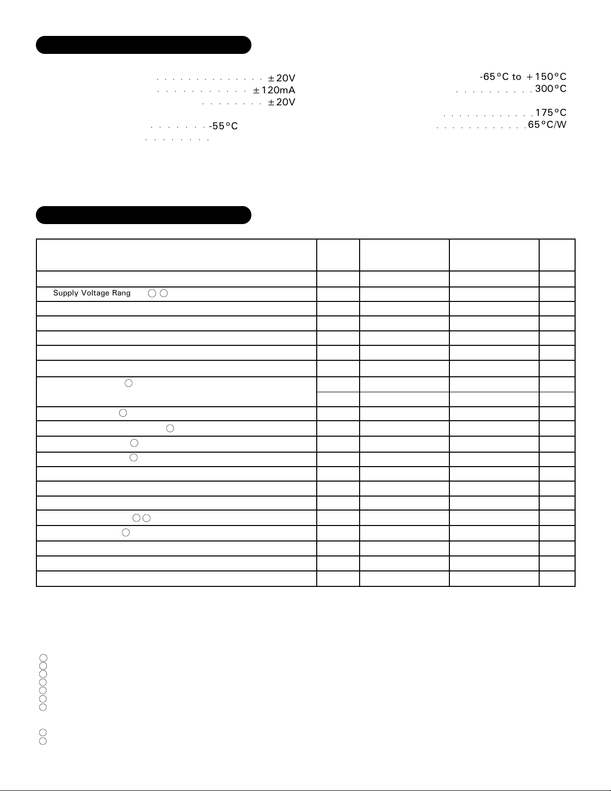
EQUIVALENT SCHEMATIC
TYPICAL APPLICATIONS
Sample And Hold
Impedance Buffers For A to D's
High Speed Line Drivers
CRT Deflection Driver
PIN-OUT INFORMATION
Positive Driver Power
1
Supply
2
N/C
3
N/C
4
N/C
5
Input
6
Offset Preset
1 Rev. B 7/00
Offset Adjust
7
N/C
8
Negative Driver Power Supply
9
Negative Power Supply
10
Output
11
Positive Power Supply
12
ABSOLUTE MAXIMUM RATINGS
±VCC
IOUT
VIN
TC
Supply Voltage
Output Current
○○○○○○○○○○○○○○
○○○○○○○○○○○
Differential Input Voltage
Case Operating Temperature
(MSK 0033B)
(MSK 0033)
○○○○○○○
○○○○○○○○
ELECTRICAL SPECIFICATIONS
Parameter
STATIC
Supply Voltage Range
Quiescent Current
INPUT
Offset Voltage
Offset Voltage Drift
Offset Adjust
Input Bias Current 9
Input Impedance 3
Power Supply Rejection Ratio 2
Input Noise Density 3
Input Noise Voltage 3
OUTPUT
Output Voltage Swing
Output Current
Settling Time to 1% 2 3
Bandwidth (-3dB) 3
TRANSFER CHARACTERISTICS
Slew Rate
Voltage Gain
8
3
Short Pin 6 to Pin 7 VIN=0V
Short Pin 6 to Pin 7 VIN=0V
Pin 6=open RPOT=200Ω From Pin 7 to Pin 9
VIN=±10.5V RL=100Ω
RS=100Ω VIN=1VRMS F=1KHz
±120mA
○○○○○○○○
-55°C to +125°C
-40°C to +85°C
Test Conditions
VIN=0V
VCM=0V
Either Input
F=DC
±10V≤VS≤±20V
F=10Hz to 1KHz
F=1KHz
VIN=±14V RL=1KΩ
2V step
VIN=1VRMS RL=1KΩ
VOUT=±10V
±20V
±20V
TST
Storage Temperature Range
TLD
Lead Temperature Range
(10 Seconds)
TJ
Junction Temperature
RTH
Thermal Resistance
Junction to Case
Output Devices Only
Group A
Subgroup
-
1
1
2,3
1,2,3
1
2,3
-
-
-
-
4
4
-
-
4
4
MSK 0033B
Min.
±10
-
-
-
Adjust to Zero
-
-
-
65
-
-
±12.5
±12
±110
±90
-
-
1000
0.97
Typ.
±15
±19
±2.0
±25
±50
±2
10
75
1.5
40
25
140
1500
0.99
○○○○○○○○○○
○○○○○○○○○○○○
○○○○○○○○○○○○
Min.
Max.
±10
±18
±22
±10
±250
±100
±10
12
-
-
-
-
-
-
-
60
-
-
-
-
-
±12
-
±90
-
-
-
-
-
1000
-
0.95
-
-65°C to +150°C
300°C
175°C
65°C/W
MSK 0033
Typ.
±15
±19
Adjust to Zero
±50
±12.5
±110
140
1500
0.98
±5
±2
10
75
1.5
40
25
Max.
±18
±25
±15
-
-
±500
-
12
-
-
-
-
-
-
-
-
-
-
Units
V
mA
mV
µV/°C
mV
pA
nA
Ω
dB
µVRMS
nV/√Hz
V
mA
nS
MHz
V/µS
V/V
NOTES:
Unless otherwise specified ±VCC = ±15 VDC.
1
Measured within a high speed amplifier feedback loop.
2
Devices shall be capable of meeting the parameter, but need not be tested. Typical parameters are for reference only.
3
Industrial grade devices shall be tested to subgroups 1 and 4 unless otherwise specified.
4
Military grade devices ('B' suffix) shall be 100% tested to subgroups 1,2,3 and 4.
5
Subgroup 5 and 6 testing available upon request.
6
Subgroup 1,4 TA=TC=+25°C
7
Subgroup 2,5 TA=TC=+125°C
Subgroup 3,6 TA=TC=-55°C
Electrical specifications are derated for power supply voltages other than ±15VDC.
8
Measurement made 0.5 seconds after application of power. Actual DC continuous test limit is 2.5 nA at 25°C
9
2
Rev. B 7/00
 Loading...