

MSK MSK0032, MSK0032B Datasheet
ISO 9001 CERTIFIED BY DSCC
HIGH SPEED, FET INPUT
DIFFERENTIAL OP-AMP
0032
M.S.KENNEDY CORP.
4707 Dey Road Liverpool, N.Y. 13088
FEATURES:
Fast Slew Rate - 650 V/µS Typ.
FET Input
Wide Bandwidth
Electrically Isolated Case
Industry Wide Pin Compatible 0032 Upgrade
DSCC SMD 5962-80013
MIL-PRF-38534 CERTIFIED
(315) 701-6751
DESCRIPTION:
The MSK 0032 is a high speed, FET input, differential amplifier designed to replace the popular LH0032 and
TP0032. Since the MSK 0032 requires less compensation than the LH0032, it exhibits wider bandwidth and greater
stability. The MSK 0032 can be used as a direct replacement in current designs using the LH0032 or TP0032 with no
changes to compensation schemes. High frequency signal transfer circuits such as video amplifiers, high speed
integrators and comparators are just a few of the applications that the MSK 0032 is well suited for.
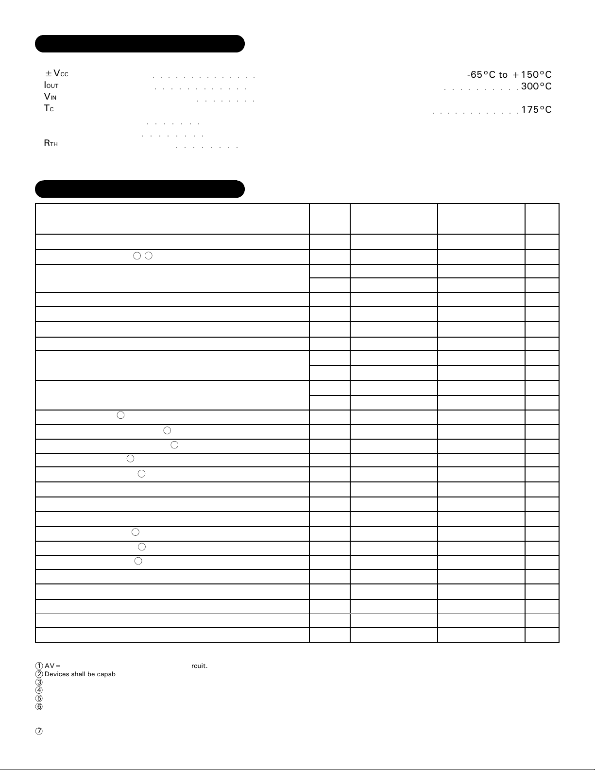
EQUIVALENT SCHEMATIC
TYPICAL APPLICATIONS
Video Amplifiers
Comparator Circuits
High Speed Integrators
PIN-OUT INFORMATION
1
No Connection
2
Output Compensation
3
Compensation/Balance
4
Compensation/Balance
5
Inverting Input
6
Non-Inverting Input
1
7
No Connection
8
No Connection
9
No Connection
10
Negative Power Supply
11
Output
12
Positive Power Supply
Rev.B 7/00
ABSOLUTE MAXIMUM RATINGS
±VCC
IOUT
VIN
TC
RTH
Supply Voltage
Output Current
Differential Input Voltage
Case Operating Temperature Range
(MSK 0032B)
(MSK 0032)
Thermal Resistance
○○○○○○○○○○○○○○
○○○○○○○○○○○○
○○○○○○○
○○○○○○○○
○○○○○○○○
Junction to Case
Output Devices Only
ELECTRICAL SPECIFICATIONS
STATIC
Supply Voltage Range
Quiescent Current
INPUT
Input Offset Voltage
Input Offset Voltage Drift
Input Offset Adjust
Input Bias Current
Input Offset Current
Input Impedance
Power Supply Rejection Ratio
Common Mode Rejection Ratio
Input Noise Voltage
Equivalent Input Noise
OUTPUT
Output Voltage Swing
Output Current
Settling Time to 1%
Settling Time to 0.1%
Unity Gain Bandwidth
TRANSFER CHARACTERISTICS
Slew Rate Limit
Open Loop Voltage Gain
Small Signal Rise Time
Small Signal Delay Time
2
7
Bal.Pins=N/C VIN=0V AV=-10V/V
2
2
2
2
2
1
1
2
±18V
±40mA
○○○○○○○○
±30V
-55°C to +125°C
-40°C to +85°C
200°C/W
Test Conditions Parameter
VIN=0V
Bal.Pins=N/C VIN=0V
RPOT=10KΩ To +VCC
VCM=0V
Either Input
VCM=0V
F=DC
∆ VCC=±15V
F=DC VCM=±10V
F=10Hz To 1MHz
F=1KHz
RL=1KΩ
RL=1KΩ
RL=1KΩ 10V step
RL=1KΩ 10V step
AV=+1
VOUT=±10V RL=1KΩ
VOUT=±10V F=100Hz
AV = +1 RL = 1KΩ
VIN = 1V RL = 1KΩ
TST
Storage Temperature Range
TLD
Lead Temperature Range
(10 Seconds)
TJ
Junction Temperature
±Vcc=±15V Unless Otherwise Specified
Group A
Subgroup
-
1
2,3
1
2,3
1,2,3
1
2,3
1
2,3
-
-
-
-
-
4
4
4
4
-
4
4
4
4
MSK 0032B MSK 0032
Min.
±10
Typ.
±15
±15
-
±18
-
±0.5
-
±10
-
Adjust to Zero Adjust to Zero
±10
-
±0.2
-
10
-
0.1
-
10
-
50
50
±10
±10
350
70
70
80
1.5
-
40
-
±12
±20
0.1
-
300
-
25
-
650
-
10
-
12
-
12
-65°C to +150°C
○○○○○○○○○○
○○○○○○○○○○○○
45
45
70
Typ.
±15
-
±15
-
-
±1
-
-
±25
-
-
-
-
-
1.5
-
-
±12
±20
0.1
-
300
-
-
650
-
-
Max.
±18
±20
±25
±5
±50
±100
±50
25
25
-
-
-
-
-
-
-
0.5
-
-
-
-
20
25
Min.
±10
±10
350
20
10
70
80
40
25
10
12
300°C
175°C
±7
0.5
20
25
Units
V
mA
mA
-
mV
µV/°C
-
mV
pA
nA
-
pA
nA
-
-
-
-
-
-
-
-
Ω
dB
dB
µVrms
nV√Hz
V
mA
µS
nS
-
MHz
-
V/µS
-
dB
-
nS
nS
Max.
±18
±22
-
-
±300
-
100
-
12
-
NOTES:
1
AV=-1, measured in false summing junction circuit.
2
Devices shall be capable of meeting the parameter, but need not be tested. Typical parameters are for reference only.
3
Industrial grade devices shall be tested to subgroups 1 and 4 unless otherwise specified.
4
Military grade devices ('B' suffix) shall be 100% tested to subgroups 1,2,3 and 4.
5
Subgroup 5 and 6 testing available upon request.
6
Subgroup 1,4 TA=TC=+25°C
Subgroup 2,5 TA=TC=+125°C
Subgroup 3,6 TA=TC=-55°C
7
Electrical specifications are derated for power supply voltages other than ±15VDC.
Rev.B 7/002
 Loading...