

MSK MSK0002, MSK0002H Datasheet
ISO 9001 CERTIFIED BY DSCC
HIGH SPEED, BUFFER
AMPLIFIER AMP
0002
M.S.KENNEDY CORP.
4707 Dey Road Liverpool, N.Y. 13088
FEATURES:
Industry Wide LH0002 Replacement
High Input Impedance-180KΩ Min
Low Output Impedance-10Ω Max
Low Harmonic Distortion
DC to 30 MHz Bandwidth
Slew Rate is Typically 400 V/µS
Operating Range from±5V to ±20V
Available to DSCC SMD5962-7801301XC
MIL-PRF-38534 CERTIFIED
(315) 701-6751
DESCRIPTION:
The MSK 0002 is a general purpose current amplifier. It is the industry wide replacement for the LH0002. The
device is ideal for use with an operational amplifier in a closed loop configuration to increase current output. The MSK
0002 is designed with a symmetrical output stage that provides low output impedances to both the positive and
negative portions of output pulses. The MSK 0002 is packaged in a hermetic 8 lead low profile T0-5 header and is
specified over the full military temperature range.
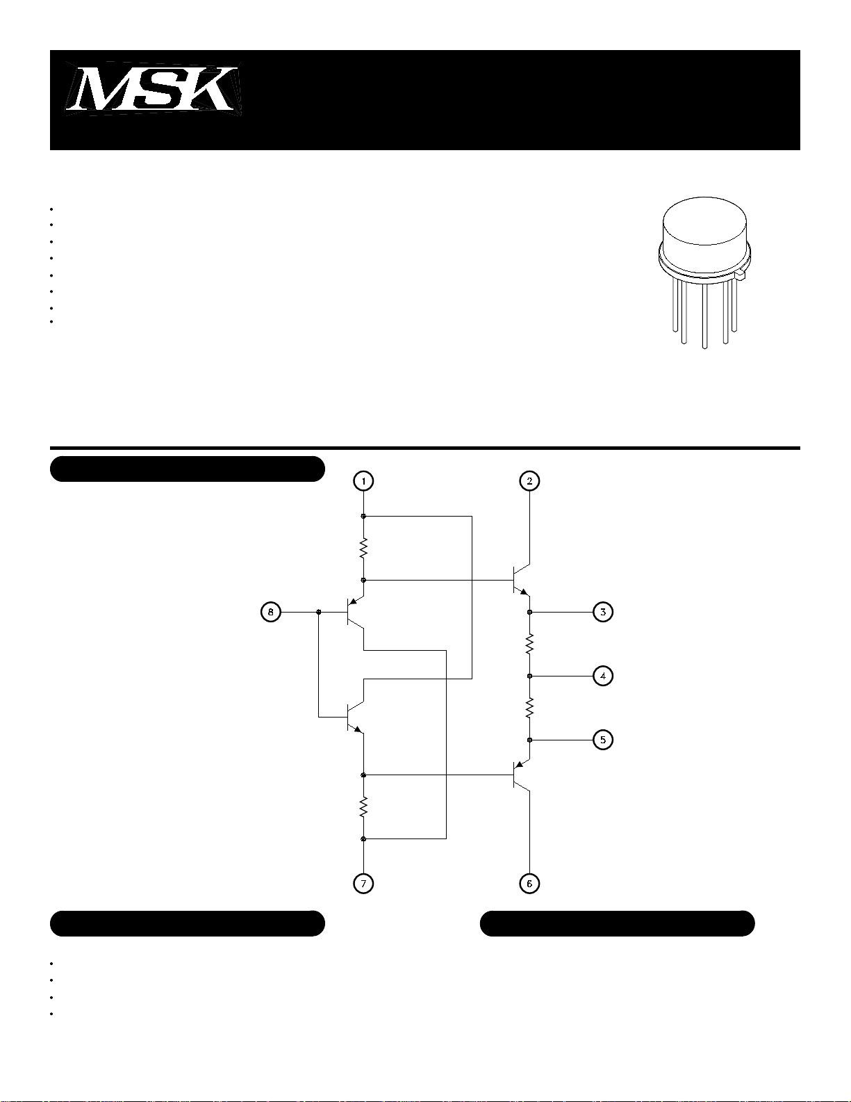
EQUIVALENT SCHEMATIC
TYPICAL APPLICATIONS
High Speed D/A Conversion
30MHz Buffer
Line Driver
Precision Current Source
PIN-OUT INFORMATION
V1+
1
V2+
2
E3
3
Output
4
1
5
E4
6
V2-
7
V1-
8
Input
Rev. - 10/00
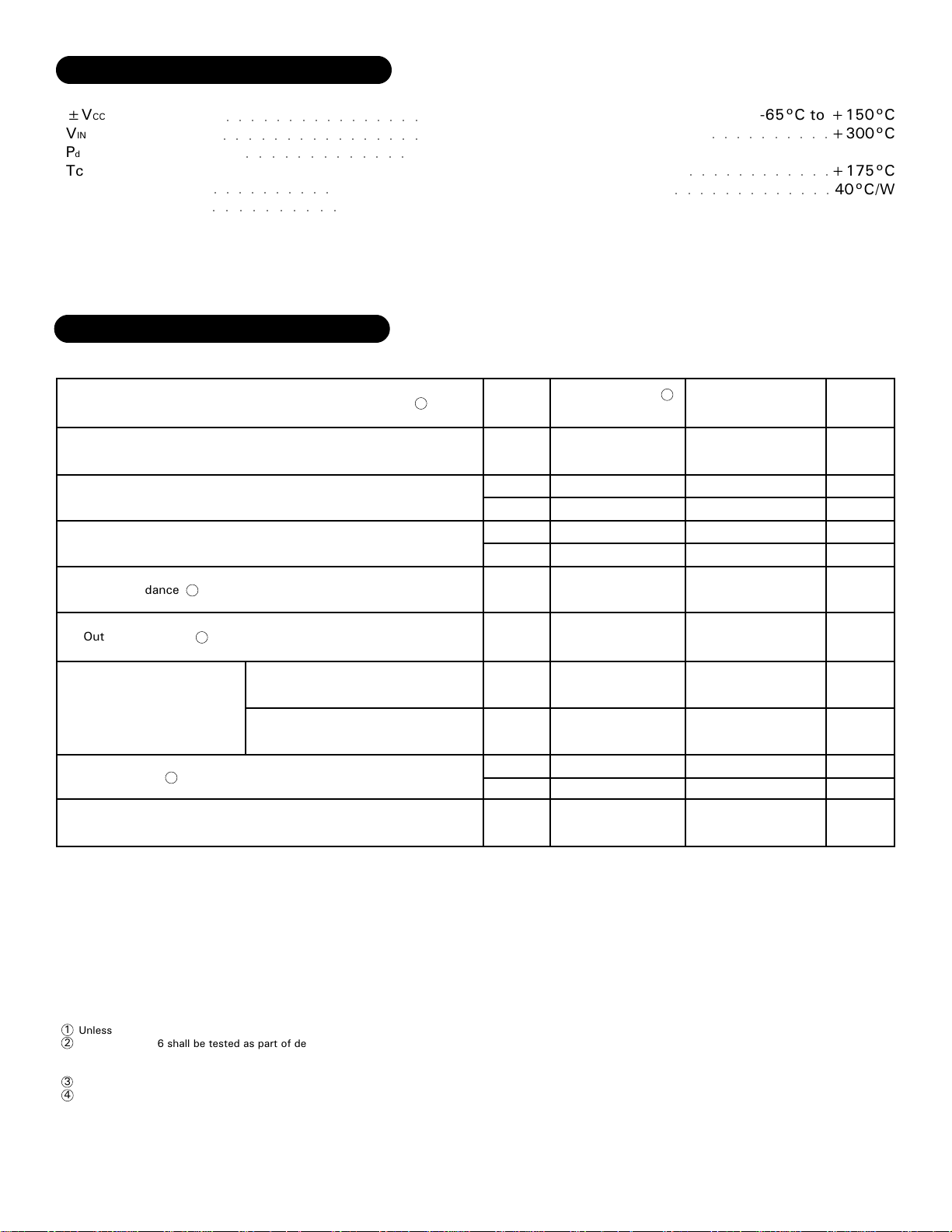
ABSOLUTE MAXIMUM RATINGS
Supply Voltage
±VCC
Input Voltage
VIN
Power Dissipation
Pd
Case Operating Temperature
Tc
(MSK 0002H)
(MSK 0002)
○○○○○○○○○○○○○○○○
○○○○○○○○○○○○○○○○
○○○○○○○○○○○○○
○○○○○○○○○○
○○○○○○○○○○
ELECTRICAL SPECIFICATIONS
±22V
±22V
600mW
-55°C to +125°C
-40°C to +85°C
TST
Storage Temperature Range
TLD
Lead Temperature Range
(10 Seconds)
TJ
Junction Temperature
θjC
Thermal Resistance
-65°C to +150°C
○○○○○○○○○○
○○○○○○○○○○○○
○○○○○○○○○○○○○
+300°C
+175°C
40°C/W
Parameter
Quiescent Current
Input Offset Current
Input Offset Voltage
Input Impedance
Output Impedance
3
3
Output Voltage Swing
Voltage Gain
2
Rise Time
Test Conditions
1
VIN=0V
RS=10KΩ RL=1.0KΩ
RS=10KΩ RL=1.0KΩ
RS=300Ω RL=1.0KΩ
VIN=1.0VRMS RS=200KΩ
RL=1KΩ f=1.0KHz
VIN=1.0VRMS Rs=10KΩ
RL=50Ω f=1.0KHz
VIN=±12Vp RL=1.0KΩ
f=1.0KHz
VIN=±10Vp RL=100Ω
+VCC=±15V f=1.0KHz
VIN=3.0VPP f=1.0KHz
RS=10KΩ RL=1.0KΩ
VOUT=2.5VPP f=10KHz
RS=100Ω RL=50Ω
Group A
Subgroup
1
1
2,3
1
2,3
4
4
4
4
4
5,6
4
MSK 0002H
Min. Typ. Max.
±6.3
±2
±2
±6
±10
-
-
±11
-
0.97
-
8
±10
±10
±10
±30
±30
10
12
-
-
-
-
-
180
-
±10
±9.5
0.95
0.95
-
4
MSK 0002
Min. Typ. Max.
-
-
-
-
-
-
180
-
-
±10
-
±9.5
0.95
-
-
-
-
±6.3
±2
-
±6
-
-
-
±11
-
0.97
-
8
±10
±10
-
±30
-
-
10
-
-
-
-
12
Units
mA
µA
µA
mV
mV
KΩ
Ω
Vp
Vp
V/V
V/V
nS
NOTES:
1
Unless otherwise specified ±V
2
Subgroups 5 & 6 shall be tested as part of device initial characterization and after design
and process changes. Parameter shall be guaranteed to the limits specified for subgroups
5 & 6 for all lots not specifically tested.
3
Devices shall be capable of meeting the parameter, but need not be tested.
4
Subgroup 1,4 TA=TC=+25°C
Subgroup 2,5 TA=TC=+125°C
Subgroup 3,6 TA=TC=-55°C
CC=±12VDC
Rev. - 10/002
 Loading...