

MSK BBF2815SK, BBF2815SH, BBF2815SE, BBF2815S, BBF2812SK Datasheet
...
HI-REL DESIGN
REPLACES APEX DB2800S SERIES
SURFACE MOUNT MAGNETICS
WELDED HERMETIC PACKAGE
LOW INTERNAL TEMPERATURE GRADIENTS
ALL CERAMIC CAPACITORS
WITHSTANDS 5000G
OTHER FEATURESSINGLE OUTPUT
NO DERATING 55°C to +125°C
OUTPUT VOLTAGE ADJUSTMENT STANDARD
REMOTE SHUTDOWN
DESCRIPTION
The BBF2800S series of DC-DC converters provides the
ruggedness, reliability and features required to meet the
advanced design challenges of today’s hi-rel market. This has
been accomplished using a package having very low thermal
gradients, excellent hermeticity and high voltage isolation.
The use of advanced substrate and reflow soldering techniques during construction results in a rugged, cost-effective
pin solderable package.
The BBF2800S hybrid converter series utilizes all ceramic
capacitors and surface mount magnetics to provide reliable
operation at all operating temperatures while surviving very
high G forces.
BBF2800S series standard features include kelvin sense,
indefinite short circuit protection, remote shutdown, output
fault monitoring, turn on voltage point adjustment, switching
frequency synchronization of up to 3 units using no external
components and pi-network input filtering. An output voltage
adjustment/load compensation pin is also standard.
Fault tolerant design protects these converters from most
external circuit faults. The output and output adjust pins will
withstand +35V while the shutdown and all synchronization
pins will withstand +50V protecting the converters from a
variety of system or board faults, i.e. solder bridges, etc.
Unique load fault protection circuitry allows this converter to
pull up loads having difficult static load line characteristics and
allows short term load excursions significantly beyond ratings
in most applications.
The BBF2800 series is a current mode push-pull topology
converter which operates at a switching frequency of 500KHz.
Internal filtering of both input and output eliminates the need for
external capacitors in many applications.
The 12-pin power dip package allows connection to a
heatsink and is hermetically sealed and isolated from the
internal circuits.
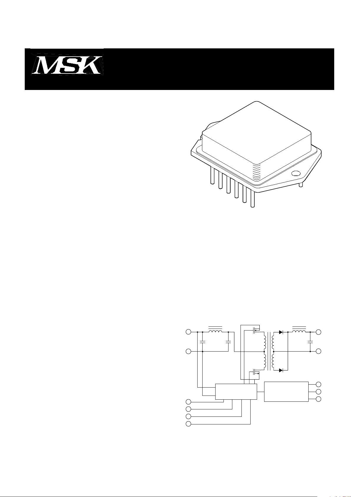
P W M
CURRENT MODE
CONTROLLER
ERROR AMPLIFIER
REFERENCE AND
ISOLATION
8
7
5
6
1
2
3
10
11
12
4
BLOCK DIAGRAM
4707 Dey Road Liverpool, N.Y. 13088
M.S.KENNEDY CORP.
(315) 701-6751
BBF2800S
SERIES
ISO-9001 CERTIFIED BY DSCC
20W
DC-DC
CONVERTERS
Rev. - 3/011
EXTERNAL CONNECTIONS
1
2
3
4
5
6
+INPUT
SHUTDOWN PLUS
CLOCK
ADJUST/COMP
-OUTPUT
+OUTPUT
12
11
10
9
8
7
-INPUT
TIMING 2
TIMING 1
CASE
-SENSE
+SENSE

BBF2803S
ABSOLUTE MAXIMUM RATINGS
SPECIFICATIONS
ABSOLUTE MAXIMUM
RATINGS
INPUT VOLTAGE RANGE (Pin 12 to 1, 2, 3, 10 or 11) 0 - 50 Vdc
INPUT TRANSIENT (Pin 12 to 1) 80 V @ 50 ms
OUTPUT WITHSTAND (Pin 5 and 8 to 7, 6 or 4) 35 Vdc
OUTPUT CURRENT (Continuous) 5.5 Adc BBF2803S
4.0 Adc BBF2805S
1.9 Adc BBF2812S
1.5 Adc BBF2815S
TEMPERATURE, Storage –65
o
C, 150oC
TEMPERATURE, Pin Soldering 10s 300oC
NOTES: 1. Unless otherwise stated: TC = 25°, VIN = 28V, I
OUT
= I
MAX AMPS
2. Derate power linearly to zero from 125°C to 135°C.
3. Regulation measured between pin 8 and pin 7.
4. Recovery spec assumes that converter has been OFF for at least 500ms.
CAUTION: The internal substrate contains beryllia (BeO). Do not break the seal. If accidentally broken, do not crush, machine, or
subject to temperatures in excess of 850°C to avoid generating toxic fumes.
CAUTION
SPECIFICATIONS
BBF2803S
PARAMETER TEST CONDITIONS
1
MIN TYP MAX UNITS
STEADY STATE CHARACTERISTICS
INPUT VOLTAGE RANGE 16 28 40 Vdc
OUTPUT VOLTAGE VIN; min to max Vdc @ I
MIN
3.2 3.3 3.4 Vdc
OUTPUT CURRENT VIN; min to max Vdc 500 5500 mAdc
EFFICIENCY 66 %
OUTPUT RIPPLE VOLTAGE Bandwidth 10 kHz to 1MHz 20 50 mVrms
INPUT RIPPLE CURRENT Bandwidth 10 kHz to 1MHz 20 50 mArms
OUTPUT POWER
2
1.6 18.0 W
LINE REGULATION
3
VIN; min to max
3
2 20 mVdc
LOAD REGULATION
3
I
OUT
; min to max
3
1 15 mVdc
TEMPERATURE COEFFICIENT .01 %/°C
TEMPERATURE RANGE, case
2
–55 125 °C
QUIESCENT CURRENT I
OUT
= 0 A 35 40 mAdc
INHIBITED V
PIN5
; < 8 Vdc .09 1.25 2.5 mAdc
ISOLATION CHARACTERISTICS
(INPUT/OUTPUT/CASE)
LEAKAGE RESISTANCE (V
TEST
= 500Vdc) 100 MΩ
LEAKAGE CAPACITANCE (f = 10kHz) 50 pF
DYNAMIC CHARACTERISTICS
LINE STEP RESPONSE V
IN; TR
, TF = 10µs
VOLTAGE CHANGE VIN; 16 to 40 Vdc 300 mV
RECOVERY TIME (95%) 30 µs
WITH 100µF OUTPUT CAP
VOLTAGE CHANGE VIN; 16 to 40 Vdc 100 mV
RECOVERY TIME (95%) 100 µs
LOAD STEP RESPONSE I
OUT; TR
, TF = 10µs
VOLTAGE CHANGE I
OUT
; 50% to max Adc 1400 m V
RECOVERY TIME (95%) 40 µs
WITH 100µF OUTPUT CAP
VOLTAGE CHANGE I
OUT
; 50% to max Adc 300 mV
RECOVERY TIME (95%) 60 µs
START-UP OVERSHOOT VIN ; 0 to 40 Vdc 0 mV
SHUTDOWN DELAY V
PIN5
; > 10 Vdc to < 8 Vdc 220 500 µs
SHUTDOWN RECOVERY
4
V
PIN5
; < 8 Vdc to > 10 Vdc 30 60 mS
Rev. - 3/012

SPECIFICATIONS
BBF2805S BBF2812S BBF2815S
BBF2805S BBF2812S BBF2815S
MIN TYP MAX MIN TYP MAX MIN TYP MAX UNITS
16 28 40 16 28 40 16 28 40 Vdc
5.00 5.05 5.1 12.00 12.05 12.1 15.0 15.1 15.2 Vdc
400 4000 190 1900 150 1500 mAdc
70 72 73 %
20 50 25 50 25 50 mVrms
20 30 20 30 20 30 mArms
2 20 2.3 23 2.2 22 W
5 50 5 50 10 50 mVdc
2 25 5 50 20 50 mVdc
.01 .01 .01 %/°C
–55 125 –55 125 –55 125 °C
35 40 35 40 35 40 mAdc
.09 1.25 2.5 .09 1.25 2.5 .9 1.25 2.5 mAdc
100 100 100 MΩ
50 80 85 pF
400 300 300 mV
30 40 40 µs
200 150 150 mV
250 250 250 µs
1400 800 800 mV
40 60 60 µs
500 280 280 mV
150 400 400 µs
000mV
220 500 220 500 220 500 µs
30 60 30 60 30 60 ms
PACKAGE THERMAL SPECIFICATIONS MIN TYP MAX UNITS
RESISTANCE, case to air 12 °C/W
TEMPERATURE RISE, junction to case 10 15 °C
Rev. - 3/013
 Loading...