

Page 1
8
+12V_BUS
C1
CAP CER 10UF 20% 16V X5R
10UFC110UF
(1206)1.8MM H MAX
+12V_BUS
+12V_BUS
C2
D D
+3.3V_BUS
+3.3V_BUS
C C
B B
C3
150nF_16VC2150nF_16V
150nF_16VC3150nF_16V
CAP CER 10UF 10% 6.3V X6S
(0805)1.4MM MAX THI C K
C5
10uF_X6SC510uF_X6S
C8
C7
C6
1uF_6.3VC71uF_6.3V
100nF_6.3VC6100nF_6.3V
Place these caps as close to the PCIE
connector as possible
10nFC810nF
7
+3.3V
R5
R6
NC_4.7KR5NC_4.7K
NC_4.7KR6NC_4.7K
C9
C9
DNIDNI
NC_100nF_6.3V
GPIO_4(7)
GPIO_3(7)
TEST_EN_J TEST_EN_J
NC_100nF_6.3V
R10RR1
0R
(2)
+3.3V_BUS
PETn0_GFXRn0(2)
PETp1_GFXRp1
PETn1_GFXRn1(2)
PETp2_GFXRp2(2)
PETn2_GFXRn2(2)
PETp3_GFXRp3(2)
PETn3_GFXRn3(2)
PETp4_GFXRp4(2)
PETn4_GFXRn4(2)
PETp5_GFXRp5(2)
PETn5_GFXRn5(2)
PETp6_GFXRp6(2)
PETn6_GFXRn6(2)
PETp7_GFXRp7(2)
PETn7_GFXRn7(2)
PETp8_GFXRp8(2)
PETn8_GFXRn8(2)
PETp9_GFXRp9(2)
PETn9_GFXRn9(2)
PETp10_GFXRp10(2)
PETn10_GFXRn10(2)
PETp11_GFXRp11(2)
PETn11_GFXRn11(2)
PETp12_GFXRp12(2)
PETn12_GFXRn12(2)
PETp13_GFXRp13(2)
PETn13_GFXRn13(2)
PETp14_GFXRp14(2)
PETn14_GFXRn14(2)
PETp15_GFXRp15(2)
PETn15_GFXRn15(2)
6
U12
U12
VCC8OE1
1B2OE2
6
2B
1A
4
2A
GND
NC_NC7WB66K8X
NC_NC7WB66K8X
NC_0RR7NC_0R
R7
NC_0RR8NC_0R
R8
DNI , To Bypass U12
+3.3V_BUS
JTRST
PRESENCE
5
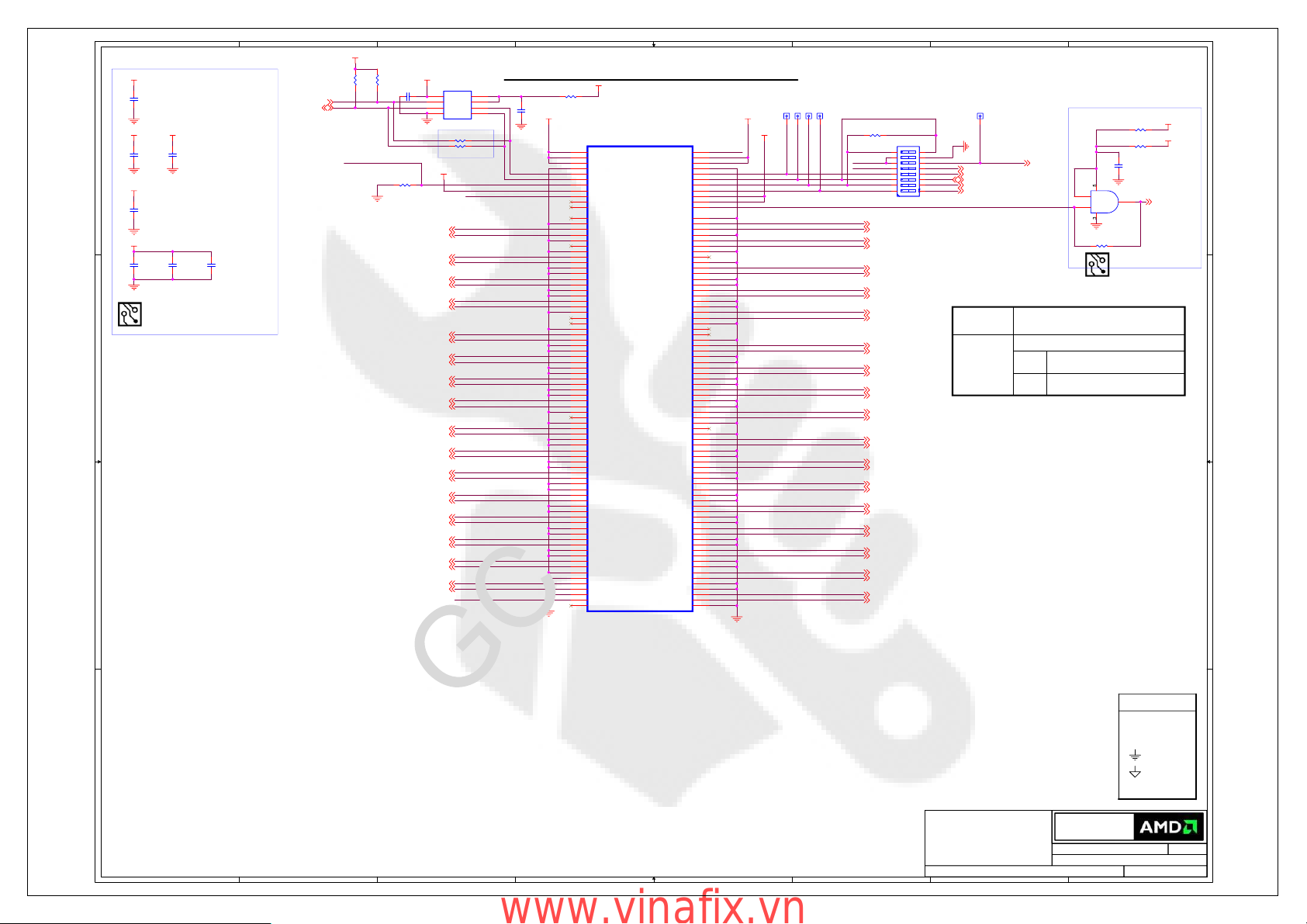
PCI-EXPRESS EDGE CONNECTOR
7
3
1
5
C10
C10
NC_100nF_6.3V
NC_100nF_6.3V
SMCLK
SMDAT
+12V_BUS
+3.3V
R4
NC_0RR4NC_0R
B1
+12V#B1
B2
+12V#B2
B3
+12V#B3
B4
GND#B4
B5
SMCLK
B6
SMDAT
B7
GND#B7
B8
+3.3V#B8
B9
JTAG1
B10
3.3Vaux
B11
WAKE#
Mechanical Key
B12
B13
B14
B15
B16
B17
B18
B19
B20
B21
B22
B23
B24
B25
B26
B27
B28
B29
B30
B31
B32
B33
B34
B35
B36
B37
B38
B39
B40
B41
B42
B43
B44
B45
B46
B47
B48
B49
B50
B51
B52
B53
B54
B55
B56
B57
B58
B59
B60
B61
B62
B63
B64
B65
B66
B67
B68
B69
B70
B71
B72
B73
B74
B75
B76
B77
B78
B79
B80
B81
B82
Mechanical Key
RSVD#B12
GND#B13
PETp0
PETn0
GND#B16
PRSNT2#B17
GND#B18
PETp1
PETn1
GND#B21
GND#B22
PETp2
PETn2
GND#B25
GND#B26
PETp3
PETn3
GND#B29
RSVD#B30
PRSNT2#B31
GND#B32
PETp4
PETn4
GND#B35
GND#B36
PETp5
PETn5
GND#B39
GND#B40
PETp6
PETn6
GND#B43
GND#B44
PETp7
PETn7
GND#B47
PRSNT2#B48
GND#B49
PETp8
PETn8
GND#B52
GND#B53
PETp9
PETn9
GND#B56
GND#B57
PETp10
PETn10
GND#B60
GND#B61
PETp11
PETn11
GND#B64
GND#B65
PETp12
PETn12
GND#B68
GND#B69
PETp13
PETn13
GND#B72
GND#B73
PETp14
機
PETn14
GND#B76
GND#B77
PETp15
PETn15
GND#B80
PRSNT2#B81
RSVD#B82
x16 PCIe
x16 PCIe
PRSNT1#A1
+12V#A2
+12V#A3
GND#A4
JTAG2
JTAG3
JTAG4
JTAG5
+3.3V#A9
+3.3V#A10
PERST#
GND#A12
REFCLK+
REFCLKGND#A15
PERp0
PERn0
GND#A18
RSVD#A19
GND#A20
PERp1
PERn1
GND#A23
GND#A24
PERp2
PERn2
GND#A27
GND#A28
PERp3
PERn3
GND#A31
RSVD#A32
RSVD#A33
GND#A34
PERp4
PERn4
GND#A37
GND#A38
PERp5
PERn5
GND#A41
GND#A42
PERp6
PERn6
GND#A45
GND#A46
PERp7
PERn7
GND#A49
RSVD#A50
GND#A51
PERp8
PERn8
GND#A54
GND#A55
PERp9
PERn9
GND#A58
GND#A59
PERp10
密
PERn10
GND#A62
GND#A63
PERp11
PERn11
GND#A66
GND#A67
PERp12
PERn12
GND#A70
GND#A71
PERp13
PERn13
GND#A74
GND#A75
PERp14
PERn14
GND#A78
GND#A79
PERp15
PERn15
GND#A82
MPCIE1
MPCIE1
A1
A2
A3
A4
A5
A6
A7
A8
A9
A10
A11
A12
A13
A14
A15
A16
A17
A18
A19
A20
A21
A22
A23
A24
A25
A26
A27
A28
A29
A30
A31
A32
A33
A34
A35
A36
A37
A38
A39
A40
A41
A42
A43
A44
A45
A46
A47
A48
A49
A50
A51
A52
A53
A54
A55
A56
A57
A58
A59
A60
A61
A62
A63
A64
A65
A66
A67
A68
A69
A70
A71
A72
A73
A74
A75
A76
A77
A78
A79
A80
A81
A82
PRESENCE
4
TP2
TP2
TP1
TP1
TP5
TP5
35mil
35mil
35mil
35mil
35mil
+12V_BUS
+3.3V_BUS
JTCK
JTDI
JTDO
JTMS
PERp0
PERn0
PERp1
PERn1
PERp2
PERn2
PERp3
PERn3
PERp4
PERn4
PERp5
PERn5
PERp6
PERn6
文件
PERp7
PERn7
PERp8
PERn8
PERp9
PERn9
PERp10
PERn10
PERp11
PERn11
PERp12
PERn12
PERp13
PERn13
PERp14
PERn14
PERp15
PERn15
35mil
3
TP3
TP3
35mil
35mil
No JTAG
R2 0RR2 0R
NC_TDA08H0SB1R
NC_TDA08H0SB1R
JTRST
TSW1
TSW1
PCIE_REFCLKP (2)
PCIE_REFCLKN (2)PETp0_GFXRp0(2)
PERp0 (2)
PERn0 (2)
PERp1 (2)
PERn1 (2)
PERp2 (2)
PERn2 (2)
PERp3 (2)
PERn3 (2)
PERp4 (2)
PERn4 (2)
PERp5 (2)
PERn5 (2)
PERp6 (2)
PERn6 (2)
PERp7 (2)
PERn7 (2)
PERp8 (2)
PERn8 (2)
PERp9 (2)
PERn9 (2)
PERp10 (2)
PERn10 (2)
PERp11 (2)
PERn11 (2)
PERp12 (2)
PERn12 (2)
PERp13 (2)
PERn13 (2)
PERp14 (2)
PERn14 (2)
PERp15 (2)
PERn15 (2)
2
TP4
TP4
35mil
35mil
98
107
116
125
134
143
152
161
JTAG_TRSTB (7)
JTAG_TCK (7)
JTAG_TDI (7)
JTAG_TDO (7)
JTAG_TMS (7)
PERST#
JTAG_MODE
JTAG_MODE (7)
1
2
R3 NC_0RR3 NC_0R
1
R9 & MR9 can share pa d
R9 0RR9 0R
MR9 NC_0RMR9 NC_0R
C4
100nF_6.3VC4100nF_6.3V
NC7SZ08P5X_NL
NC7SZ08P5X_NL
4
U11
U11
R_RST
DNI
+3.3V_BUS
+3.3V
PERST#_buf (2,11,17)
Place R3 in U5
Table 1: Connection for JTAG
Production
(No JTAG)
Internal Use Only
TSW1, R1 & R2 are located on the bottom side of the board close to PCIE con necto r.
Install R1, R2 & Don't Install TSW1
Install TSW1 & Don't Install R1 & R2
TSW1 Switch #1, 2, 3, 4, 5 and 6 close d (ON)
JTAG
#8 and 7 open
TSW1 Switch #1, 2, 3, 4, 5 and 6 open
NO JTAG
#8 & 7 closed (ON)
A A
8
7
Printed with FinePrint - purchase at www.fineprint.com
SYMBOL LEGEND
DO NOT
DNI
INSTALL
ACTIVE
#
LOW
DIGITAL
GROUND
ANALOG
GROUND
BUO BRING UP
Doc No.
Doc No.
Doc No.
1
ONLY
RevDate:
RevDate:
RevDate:
1
1
1
105-B507xx-10
105-B507xx-10
105-B507xx-10
HD4870XG5-v10
CONFIDENTIAL & PROPRIETARY TO ADVANCED MICRO DEVICES INC.
CONFIDENTIAL & PROPRIETARY TO ADVANCED MICRO DEVICES INC.
CONFIDENTIAL & PROPRIETARY TO ADVANCED MICRO DEVICES INC.
?2007 Advanced Micro D evices
?2007 Advanced Micro D evices
?2007 Advanced Micro D evices
This AMD Board schemat ic and desi gn is the exclu sive pr opert y o f AMD,
This AMD Board schemat ic and desi gn is the exclu sive pr opert y o f AMD,
This AMD Board schemat ic and desi gn is the exclu sive pr opert y o f AMD,
and is provided only to entiti es under a non -disclosure agreement
and is provided only to entiti es under a non -disclosure agreement
and is provided only to entiti es under a non -disclosure agreement
with AMD for evalu ation purposes. F urther distribut ion or di sclosure
with AMD for evalu ation purposes. F urther distribut ion or di sclosure
with AMD for evalu ation purposes. F urther distribut ion or di sclosure
is strictly prohibited. Use of th is sch ematic and de sign fo r any pu rpose
is strictly prohibited. Use of th is sch ematic and de sign fo r any pu rpose
is strictly prohibited. Use of th is sch ematic and de sign fo r any pu rpose
other than evaluation re quires a Board T echnology License Agre ement
other than evaluation re quires a Board T echnology License Agre ement
other than evaluation re quires a Board T echnology License Agre ement
with AMD. AMD makes no r epre sentat ions or war ranties of an y kind
with AMD. AMD makes no r epre sentat ions or war ranties of an y kind
with AMD. AMD makes no r epre sentat ions or war ranties of an y kind
regarding this schemat ic and design , in cluding, n ot limit ed to,
regarding this schemat ic and design , in cluding, n ot limit ed to,
regarding this schemat ic and design , in cluding, n ot limit ed to,
any implied warranty of mer chanti bility or fitness for a par ticular
any implied warranty of mer chanti bility or fitness for a par ticular
any implied warranty of mer chanti bility or fitness for a par ticular
purpose, and disclaims respons ibility forany co nsequences resul ting
purpose, and disclaims respons ibility forany co nsequences resul ting
purpose, and disclaims respons ibility forany co nsequences resul ting
from use of the information include d herein .
from use of the information include d herein .
from use of the information include d herein .
Title
Title
6
5
4
3
Title
RH RV770 GDDR5 DVI-I VO DVI-I FH
RH RV770 GDDR5 DVI-I VO DVI-I FH
RH RV770 GDDR5 DVI-I VO DVI-I FH
2
Advanced Micro Devices Inc.
Advanced Micro Devices Inc.
Advanced Micro Devices Inc.
1 Commerce Valley Drive East
1 Commerce Valley Drive East
1 Commerce Valley Drive East
Markham, Ontario
Markham, Ontario
Markham, Ontario
Thursday, October 09, 2008
Thursday, October 09, 2008
Thursday, October 09, 2008
Sheet
Sheet
Sheet
122
122
122
of
of
of
www.vinafix.vn
Page 2
5
NOTE: some of the PCIE test point s wil l
be available trought via on traces.
1uF_6.3V
1uF_6.3V
C99
C99
TP15TP15
TP8TP8
TP9TP9
TP16TP16
TP18TP18
TP12TP12
TP20TP20
TP21TP21
TP25TP25
TP27TP27
C91
C91
100nF_6.3V
100nF_6.3V
C100
C100
1uF_6.3V
1uF_6.3V
TP6TP6
TP13TP13
TP14TP14
TP7TP7
TP17TP17
TP10TP10
TP11TP11
TP19TP19
TP22TP22
TP23TP23
TP26TP26
C92
C92
+PCIE_VDDC
1uF_6.3V
1uF_6.3V
D D
C C
PCIE_REFCLKP(1)
PCIE_REFCLKN(1)
+1.1V +PCIE_VDDC
B B
B23
B23
+PCIE_VDDR+1.8V
26R_600mA
26R_600mA
4.7uF_6.3V
4.7uF_6.3V
A A
PETp0_GFXRp0(1)
PETn0_GFXRn0(1)
PETp1_GFXRp1(1)
PETn1_GFXRn1(1)
PETp2_GFXRp2(1)
PETn2_GFXRn2(1)
PETp3_GFXRp3(1)
PETn3_GFXRn3(1)
PETp4_GFXRp4(1)
PETn4_GFXRn4(1)
PETp5_GFXRp5(1)
PETn5_GFXRn5(1)
PETp6_GFXRp6(1)
PETn6_GFXRn6(1)
PETp7_GFXRp7(1)
PETn7_GFXRn7(1)
PETp8_GFXRp8(1)
PETp9_GFXRp9(1)
PETn9_GFXRn9(1)
PETp10_GFXRp10(1)
PETn10_GFXRn10(1)
PETp11_GFXRp11(1)
PETn11_GFXRn11(1)
PETp12_GFXRp12(1)
PETn12_GFXRn12(1)
PETp13_GFXRp13(1)
PETn13_GFXRn13(1)
PETp14_GFXRp14(1)
PETn14_GFXRn14(1)
PETp15_GFXRp15(1)
PETn15_GFXRn15(1)
B21220R_2A B21220R_2A
10uF_X6S
10uF_X6S
C94
C94
1uF_6.3V
1uF_6.3V
C88
C88
C51
C51
1uF_6.3V
1uF_6.3V
C95
C95
C96
C96
100nF_6.3V
100nF_6.3V
1uF_6.3V
1uF_6.3V
5
1uF_6.3V
1uF_6.3V
C97
C97
C90
C90
C89
C89
1uF_6.3V
1uF_6.3V
C98
C98
1uF_6.3V
1uF_6.3V
1uF_6.3V
1uF_6.3V
1uF_6.3V
1uF_6.3V
C101
C101
4
U1A
U1A
AM48
PCIE_RX0P
AL49
PCIE_RX0N
AL51
PCIE_RX1P
AK52
PCIE_RX1N
AK48
PCIE_RX2P
AJ49
PCIE_RX2N
AJ51
PCIE_RX3P
AH52
PCIE_RX3N
AH48
PCIE_RX4P
AG49
PCIE_RX4N
AG51
PCIE_RX5P
AF52
PCIE_RX5N
AF48
PCIE_RX6P
AE49
PCIE_RX6N
AE51
PCIE_RX7P
AD52
PCIE_RX7N
AD48
PCIE_RX8P
AC49
PCIE_RX8N
AC51
PCIE_RX9P
AB52
PCIE_RX9N
AB48
PCIE_RX10P
AA49
PCIE_RX10N
AA51
PCIE_RX11P
Y52
PCIE_RX11N
Y48
PCIE_RX12P
W49
PCIE_RX12N
W51
PCIE_RX13P
V52
PCIE_RX13N
V48
PCIE_RX14P
U49
PCIE_RX14N
U51
PCIE_RX15P
T52
PCIE_RX15N
AM45
PCIE_REFCLKP
AM44
AA38
AA39
AB37
AB38
AB39
AD37
AD38
AD39
AE37
AE38
AE39
AM40
AH37
AK38
AK39
AK37
AM37
AM38
AM39
AN37
AN38
AN39
AR39
AR40
AA40
AA43
AA47
AB50
AB40
AB43
AC53
AC47
AD50
AD40
AD43
AE53
AE40
AE43
AE47
AG53
AG47
AF39
AF38
AF37
W38
W39
W40
W41
W42
W43
W44
W45
AJ38
AJ39
AJ37
AF50
AF40
AF43
PCIE_REFCLKN
PCIE_CALRP
PCIE_CALRN
PCIE_VDDC#1
PCIE_VDDC#2
PCIE_VDDC#3
PCIE_VDDC#4
PCIE_VDDC#5
PCIE_VDDC#6
PCIE_VDDC#7
PCIE_VDDC#8
PCIE_VDDC#9
PCIE_VDDC#10
PCIE_VDDC#11
PCIE_VDDC#12
PCIE_VDDC#13
PCIE_VDDC#14
PCIE_VDDC#15
PCIE_VDDC#16
PCIE_VDDC#17
PCIE_VDDC#18
PCIE_VDDC#19
PCIE_VDDC#20
PCIE_VDDR#1
PCIE_VDDR#2
PCIE_VDDR#3
PCIE_VDDR#4
PCIE_VDDR#5
PCIE_VDDR#6
PCIE_VDDR#7
PCIE_VDDR#8
PCIE_VDDR#9
PCIE_VDDR#10
PCIE_VDDR#11
PCIE_VDDR#12
PCIE_VDDR#13
PCIE_VDDR#14
PCIE_VDDR#15
PCIE_VDDR#16
PCIE_VSS#1
PCIE_VSS#2
PCIE_VSS#3
PCIE_VSS#4
PCIE_VSS#5
PCIE_VSS#6
PCIE_VSS#7
PCIE_VSS#8
PCIE_VSS#9
PCIE_VSS#10
PCIE_VSS#11
PCIE_VSS#12
PCIE_VSS#13
PCIE_VSS#14
PCIE_VSS#15
PCIE_VSS#16
PCIE_VSS#17
PCIE_VSS#18
PCIE_VSS#19
PCIE_VSS#20
R22 1.27KR22 1.27K
2.0K
2.0K
R24
R24
C93
C93
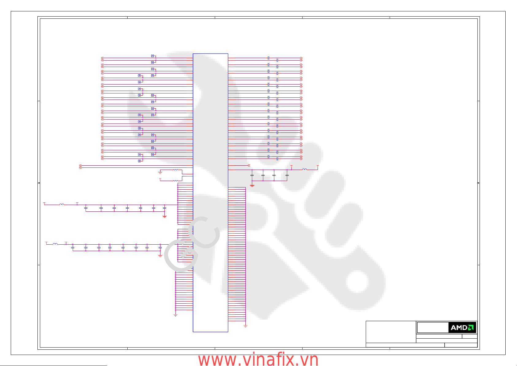
4
PCIE_TX0P
PCIE_TX0N
PCIE_TX1P
PCIE_TX1N
PCIE_TX2P
PCIE_TX2N
PCIE_TX3P
PCIE_TX3N
PCIE_TX4P
PCIE_TX4N
PCIE_TX5P
PCIE_TX5N
PCIE_TX6P
PCIE_TX6N
PCIE_TX7P
PCIE_TX7N
PCIE_TX8P
PCIE_TX8N
PCIE_TX9P
PCIE_TX9N
PCIE_TX10P
PCIE_TX10N
PCIE_TX11P
PCIE_TX11N
PCIE_TX12P
PCIE_TX12N
PCIE_TX13P
PCIE_TX13N
PCIE_TX14P
PCIE_TX14N
PCIE_TX15P
PCIE_TX15N
PCIE_PVDD
PCIE_VSS#21
PCIE_VSS#22
PCIE_VSS#23
PCIE_VSS#24
PCIE_VSS#25
PCIE_VSS#26
PCIE_VSS#27
PCIE_VSS#28
PCIE_VSS#29
PCIE_VSS#30
PCIE_VSS#31
PCIE_VSS#32
PCIE_VSS#33
PCIE_VSS#34
PCIE_VSS#35
PCIE_VSS#36
PCIE_VSS#37
PCIE_VSS#38
PCIE_VSS#39
PCIE_VSS#40
PCIE_VSS#41
PCIE_VSS#42
PCIE_VSS#43
PCIE_VSS#44
PCIE_VSS#45
PCIE_VSS#46
PCIE_VSS#47
PCIE_VSS#48
PCIE_VSS#49
PCIE_VSS#50
PCIE_VSS#51
PCIE_VSS#52
PCIE_VSS#53
PCIE_VSS#54
PCIE_VSS#55
PCIE_VSS#56
PCIE_VSS#57
PCIE_VSS#58
PCIE_VSS#59
PCIE_VSS#60
PCIE_VSS#61
PCIE_VSS#62
PCIE_VSS#63
PCIE_VSS#64
PCIE_VSS#65
PCIE_VSS#66
PCIE_VSS#67
PCIE_VSS#68
PCIE_VSS#69
PCIE_VSS#70
PCIE_VSS#71
PCIE_VSS#72
PCIE_VSS#73
PCIE_VSS#74
PCIE_VSS#75
PCIE_VSS#76
PCIE_VSS#77
PCIE_VSS#78
PCIE_VSS#79
PCIE_VSS#80
PCIE_VSS#81
PCIE_VSS#82
RV770 GL A11
RV770 GL A11
PERSTB
PCIE_TX0P
AK45
PCIE_TX0N
AK44
PCIE_TX1P
AK42
PCIE_TX1N
AK41
PCIE_TX2P
AJ45
PCIE_TX2N
AJ44
PCIE_TX3P
AJ42
PCIE_TX3N
AJ41
PCIE_TX4P
AH45
PCIE_TX4N
AH44
PCIE_TX5P
AH42
PCIE_TX5N
AH41
PCIE_TX6P
AF45
PCIE_TX6N
AF44
PCIE_TX7P
AF42
PCIE_TX7N
AF41
PCIE_TX8P
AE45
PCIE_TX8N
AE44
PCIE_TX9P
AE42
PCIE_TX9N
AE41
PCIE_TX10P
AD45
PCIE_TX10N
AD44
PCIE_TX11P
AD42
PCIE_TX11N
AD41
PCIE_TX12P
AB45
PCIE_TX12N
AB44
PCIE_TX13P
AB42
PCIE_TX13N
AB41
PCIE_TX14P
AA45
PCIE_TX14N
AA44
PCIE_TX15P
AA42
PCIE_TX15N
AA41
AT39
AR37
AH50
AH40
AH43
AJ53
AJ40
AJ43
AJ47
AK50
AK40
AK43
AL53
AL47
AM50
AA53
AM43
AN53
AN40
機
AN43
AN47
AP50
AR53
Y50
AR43
AR47
AT50
AT40
AT43
AU53
AU40
AU43
AU47
AV50
AW53
AW40
AW43
AW47
AY50
AY40
AY43
BA53
BA47
BB50
BB43
BC53
BB42
BC47
BD50
BD44
BD45
BF53
BE47
BF50
BJ53
BL45
BN46
W47
BN49
T50
U53
U47
V50
W53
3
C57
C57
C52
C52
100nF_6.3V
100nF_6.3V
100nF_6.3V
100nF_6.3V
C58
C58
100nF_6.3V
100nF_6.3V
C60
C60
100nF_6.3V
100nF_6.3V
C62
C62
100nF_6.3V
100nF_6.3V
C54
C54
100nF_6.3V
100nF_6.3V
C64
C64
100nF_6.3V
100nF_6.3V
C55
C55
100nF_6.3V
100nF_6.3V
C67
C67
100nF_6.3V
100nF_6.3V
C69
C69
100nF_6.3V
100nF_6.3V
C71
C71
100nF_6.3V
100nF_6.3V
C72
C72
100nF_6.3V
100nF_6.3V
C74
C74
100nF_6.3V
100nF_6.3V
C76
C76
100nF_6.3V
100nF_6.3V
C78
C78
100nF_6.3V
100nF_6.3V
C80
C80
100nF_6.3V
100nF_6.3V
C82
C82
100nF_6.3V
100nF_6.3V
PERST#_buf (1,11,17)
C85
C85
C86
100nF_6.3V
100nF_6.3V
C86
10uF_X6S
10uF_X6S
C84
C84
10nF
10nF
密
3
C59
C59
100nF_6.3V
100nF_6.3V
C61
C61
100nF_6.3V
100nF_6.3V
C53
C53
100nF_6.3V
100nF_6.3V
C63
C63
100nF_6.3V
100nF_6.3V
C65
C65
100nF_6.3V
100nF_6.3V
C66
C66
100nF_6.3V
100nF_6.3V
C68
C68
100nF_6.3V
100nF_6.3V
C70
C70
100nF_6.3V
100nF_6.3V
C56
C56
100nF_6.3V
100nF_6.3V
C73
C73
100nF_6.3V
100nF_6.3V
C75
C75
100nF_6.3V
100nF_6.3V
C77
C77
100nF_6.3V
100nF_6.3V
C79
C79
100nF_6.3V
100nF_6.3VTP24TP24
C81
C81
100nF_6.3V
100nF_6.3V
C83
C83
100nF_6.3V
100nF_6.3V
文件
+PCIE_PVDD +1.8V
BLM15BD121SN1
BLM15BD121SN1
B22
B22
C87
C87
1uF_6.3V
1uF_6.3V
PERp0 (1)
PERn0 (1)
PERp1 (1)
PERn1 (1)
PERp2 (1)
PERn2 (1)
PERp3 (1)
PERn3 (1)
PERp4 (1)
PERn4 (1)
PERp5 (1)
PERn5 (1)
PERp6 (1)
PERn6 (1)
PERp7 (1)
PERn7 (1)
PERp8 (1)
PERn8 (1)PETn8_GFXRn8(1)
PERp9 (1)
PERn9 (1)
PERp10 (1)
PERn10 (1)
PERp11 (1)
PERn11 (1)
PERp12 (1)
PERn12 (1)
PERp13 (1)
PERn13 (1)
PERp14 (1)
PERn14 (1)
PERp15 (1)
PERn15 (1)
2
CONFIDENTIAL & PROPRIETARY TO ADVANCED MICRO DEVICES INC.
CONFIDENTIAL & PROPRIETARY TO ADVANCED MICRO DEVICES INC.
CONFIDENTIAL & PROPRIETARY TO ADVANCED MICRO DEVICES INC.
?2007 Advanced Micro D evices
?2007 Advanced Micro D evices
?2007 Advanced Micro D evices
This AMD Board schemat ic and desi gn is the exclu sive pr opert y o f AMD,
This AMD Board schemat ic and desi gn is the exclu sive pr opert y o f AMD,
This AMD Board schemat ic and desi gn is the exclu sive pr opert y o f AMD,
and is provided only to entiti es under a non -disclosure agreement
and is provided only to entiti es under a non -disclosure agreement
and is provided only to entiti es under a non -disclosure agreement
with AMD for evalu ation purposes. F urther distribut ion or di sclosure
with AMD for evalu ation purposes. F urther distribut ion or di sclosure
with AMD for evalu ation purposes. F urther distribut ion or di sclosure
is strictly prohibited. Use of th is sch ematic and de sign fo r any pu rpose
is strictly prohibited. Use of th is sch ematic and de sign fo r any pu rpose
is strictly prohibited. Use of th is sch ematic and de sign fo r any pu rpose
other than evaluation re quires a Board T echnology License Agre ement
other than evaluation re quires a Board T echnology License Agre ement
other than evaluation re quires a Board T echnology License Agre ement
with AMD. AMD makes no r epre sentat ions or war ranties of an y kind
with AMD. AMD makes no r epre sentat ions or war ranties of an y kind
with AMD. AMD makes no r epre sentat ions or war ranties of an y kind
regarding this schemat ic and design , in cluding, n ot limit ed to,
regarding this schemat ic and design , in cluding, n ot limit ed to,
regarding this schemat ic and design , in cluding, n ot limit ed to,
any implied warranty of mer chanti bility or fitness for a par ticular
any implied warranty of mer chanti bility or fitness for a par ticular
any implied warranty of mer chanti bility or fitness for a par ticular
purpose, and disclaims respons ibility forany co nsequences resul ting
purpose, and disclaims respons ibility forany co nsequences resul ting
purpose, and disclaims respons ibility forany co nsequences resul ting
from use of the information include d herein .
from use of the information include d herein .
from use of the information include d herein .
Title
Title
Title
RH RV770 GDDR5 DVI-I VO DVI-I FH
RH RV770 GDDR5 DVI-I VO DVI-I FH
2
RH RV770 GDDR5 DVI-I VO DVI-I FH
1
Advanced Micro Devices Inc.
Advanced Micro Devices Inc.
Advanced Micro Devices Inc.
1 Commerce Valley Drive East
1 Commerce Valley Drive East
1 Commerce Valley Drive East
Markham, Ontario
Markham, Ontario
Markham, Ontario
Thursday, October 09, 2008
Thursday, October 09, 2008
Thursday, October 09, 2008
Sheet
Sheet
Sheet
222
222
222
of
of
of
1
Doc No.
Doc No.
Doc No.
RevDate:
RevDate:
RevDate:
1
1
1
105-B507xx-10
105-B507xx-10
105-B507xx-10
Printed with FinePrint - purchase at www.fineprint.com
www.vinafix.vn
Page 3
5
4
Recommended caps:
(see BOM for qualified value s/vendors)
10uF , X6S, 0805, 6.3V, 1.4MM MAX THICK
4.7uF , X6S/X5R, 0603, 6.3V/4V
1uF, X6S, 0402, 6.3V
100nF, X7R, 0402
10nF , X7R, 0402
3
2
Q102
Q102
SI2304DS
SI2304DS
1
LVT_EN(17)
1
D D
+1.8V
LVT_EN(17)
C C
+1.8V
+1.8V
B B
BLM15BD121SN1
BLM15BD121SN1
+1.8V
B108
B108
BLM15BD121SN1
BLM15BD121SN1
+1.1V
B109
B109
BLM15BD121SN1
BLM15BD121SN1
+1.8V
B110
B110
12
B118
B118
B111
B111
GND_DPLL_PVDD
C150
C150
1uF_6.3V
1uF_6.3V
A A
+1.8V
+3.3V_BUS
Install B118 & DNI
B111 for 1.8V
Oscillators
BLM15BD121SN1
BLM15BD121SN1
NC_BLM15BD121SN1
NC_BLM15BD121SN1
BLM15BD121SN1
BLM15BD121SN1
B103
B103
NS1
NS1
NS_VIA
NS_VIA
12
BLM15BD121SN1
BLM15BD121SN1
B105
B105
NS3
NS3
NS_VIA
NS_VIA
12
GND_T2PVSS
+1.8V
12
GND_A2VSSQ
+DPLL_PVDD
NS6NS_VIA NS6NS_VIA
C151
C151
100nF_6.3V
100nF_6.3V
+DPA_PVDD
MC3
MC3
4.7uF_6.3V
4.7uF_6.3V
NC_10uF_X6S
NC_10uF_X6S
Overlap footprints
+T2PVDD
BLM15BD121SN1
BLM15BD121SN1
B123
B123
+A2VDDQ
NS5NS_VIA NS5NS_VIA
1uF_6.3V
1uF_6.3V
10uF_X6S
10uF_X6S
Oscillator Option
5
SI2304DS
SI2304DS
C143
C143
C147
C147
OSC_EN(14)
Q101
Q101
C125
C125
32
C132
C132
10uF_X6S
10uF_X6S
+3.3V
1uF_6.3V
1uF_6.3V
1uF_6.3V
1uF_6.3V
+1.1V
Use 0R
10R_1A_0402
10R_1A_0402
C126
C126
1uF_6.3V
1uF_6.3V
+1.8V
+VDD1DI
12
BLM15BD121SN1
BLM15BD121SN1
C144
C144
100nF_6.3V
100nF_6.3V
C145
C145
C148
C148
OSC_EN
B102
B102
SSCLKIN(7)
10R_1A_0402
10R_1A_0402
B100
B100
4.7uF_6.3V
4.7uF_6.3V
C127
C127
100nF
100nF
C133
C133
1uF_6.3V
1uF_6.3V
BLM15BD121SN1
BLM15BD121SN1
B115
B115
NS10NS_VI A NS10NS_VIA
B106
B106
+1.8V
C146
C146
100nF_6.3V
100nF_6.3V
C149
C149
100nF_6.3V
100nF_6.3V
Y1
Y1
4
VCC
1
TRISTATE
100MHZ_1.8V
100MHZ_1.8V
+DPA_VDDR
Overlap footprints
C122
C122
MC122
MC122
NC_10uF_X6S
NC_10uF_X6S
GND_DPAVSS
C134
C134
100nF_6.3V
100nF_6.3V
+AVDD
NS9NS_VIA NS9NS_VIA
12
C371
C371
100nF_6.3V
100nF_6.3V
1uF_6.3V
1uF_6.3V
GND_VSS1DI
+A2VDD
C136
C136
4.7uF_6.3V
4.7uF_6.3V
BLM15BD121SN1
BLM15BD121SN1
B107
B107
3
OUT
2
GND
Overlap footprints
MC50
MC50
4.7uF_6.3V
4.7uF_6.3V
NC_10uF_X6S
NC_10uF_X6S
C111
C111
1uF_6.3V
1uF_6.3V
100nF_6.3V
100nF_6.3V
C368
C368
C369
C369
100nF_6.3V
100nF_6.3V
1uF_6.3V
1uF_6.3V
GND_AVSSQ
C372
C372
C373
C373
10nF
10nF
C138
C138
C137
C137
100nF_6.3V
100nF_6.3V
1uF_6.3V
1uF_6.3V
+VDD2DI
NS4NS_VIA NS4NS_VIA
12
GND_A2VSSQ
Crystal Option
3
4
C112
C112
NC_18pF_50V
NC_18pF_50V
Place holder only
Install 0R for 1.8V Osil lator s
R112
DNI for
1.8V
Osillators
4
C50
C50
+T2XVDDC
C123
C123
NC_50MHZ
NC_50MHZ
XTAL2
GND4
C370
C370
C139
C139
C140
C140
1uF_6.3V
1uF_6.3V
GND_VSS2DI
R116NC_1M R116NC_1M
XTAL1
GND2
MY1
MY1
0RR112 0R
C104
C104
1uF_6.3V
1uF_6.3V
10nF
10nF
GND_AVSSQ
10nF
10nF
1
2
R113
R113
NC_221R
NC_221R
100nF_6.3V
100nF_6.3V
XTAL1XTAL2
C117
C117
100nF
100nF
R109150R R109150R
GND_A2VSSQ
C141
C141
NC_0R
NC_0R
R117
R117
C113
C113
NC_18pF_50V
NC_18pF_50V
XTALIN
DP_CALR
R110 499RR110 499R
C142
C142
10nF
10nF
R111715R R111715R
XTALOUT
U1B
U1B
BD29
DPAVDDR#1
BE29
DPAVDDR#2
BG25
DPAVSSR#1
BN27
DPAVSSR#2
BN25
DPAVSSR#3
BG27
DPAVSSR#4
BK26
DPAVSSR#5
BK28
DPAVSSR#6
BM24
DPAVSSR#7
BD30
DPBVDDR#1
BE30
DPBVDDR#2
BK32
DPBVSSR#1
BG31
DPBVSSR#2
BN29
DPBVSSR#3
BN31
DPBVSSR#4
BH32
DPBVSSR#5
BK30
DPBVSSR#6
BG29
DPBVSSR#7
BG37
T2XVDDC#1
BK38
T2XVDDC#2
BK44
T2VXDDC#3
BM44
T2XVDDC#4
BG35
T2XVSSR#1
BN41
T2XVSSR#2
BM34
T2XVSSR#3
BG39
T2XVSSR#4
BK36
T2XVSSR#5
BJ43
T2XVSSR#6
BN43
T2XVSSR#7
BK40
T2XVSSR#8
BN35
T2XVSSR#9
BN37
T2XVSSR#10
BN39
T2XVSSR#11
BG41
T2XVSSR#12
BH42
T2XVSSR#13
BE26
DPA_PVDD
BD26
DPA_PVSS
BE28
DPB_PVDD
BD28
DPB_PVSS
BC29
DP_CALR
BN33
T2PVDD
BL33
T2PVSS
BC40
AVDD
BB40
AVSSQ
BG45
VDD1DI
BE44
VSS1DI
機
BA40
RSET
BD39
A2VDD
BC39
A2VSSQ
BD43
VDD2DI
BE43
R2SETGND_A2VSSQ
VSS2DI
BB39
R2SET
BE39
A2VDDQ
BD33
DPLL_VDDC
BG33
DPLL_PVDD
TP28
TP28
BE33
DPLL_PVSS
35mil
35mil
AV37
PLLTEST
BH44
XTALIN
BJ45
XTALOUT
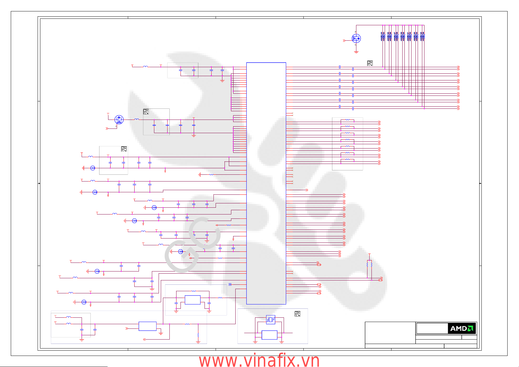
RV770 GL A11
RV770 GL A11
Multi footprint with MY1
3
4
3
BM26
TX0P_DPA2P
BL25
TX0M_DPA2N
BJ27
TX1P_DPA1P
BH26
TX1M_DPA1N
BM28
TX2P_DPA0P
BL27
TX2M_DPA0N
BJ25
TXCAP_DPA3P
BK24
TXCAM_DPA3N
BM30
TX3P_DPB2P
BL29
TX3M_DPB2N
BJ31
TX4P_DPB1P
BH30
TX4M_DPB1N
BM32
TX5P_DPB0P
BL31
TX5M_DPB0N
BJ29
TXCBP_DPB3P
BH28
TXCBM_DPB3N
BJ35
T2X0P
BH34
T2X0M
BM36
T2X1P
BL35
T2X1M
BJ37
T2X2P
BH36
T2X2M
BM38
T2X3P
BL37
T2X3M
BK34
T2XCLKP
BJ33
T2XCLKM
BM40
T2X4P
BL39
T2X4M
BJ41
T2X5P
BH40
T2X5M
BM42
NC#1
BL41
NC#2
BL43
NC#3
BK42
NC#4
BJ39
NC#5
BH38
NC#6
AW39
HPD1
密
DDC3DATA_DP3_AUX N
DDC3CLK_DP3_AUXP
DDC4CLK_DP4_AUXP
DDC4DATA_DP4_AUX N
NY1
NY1
41
32
NC_66MHz
NC_66MHz
NC_66MHz_5X7
NC_66MHz_5X7
XTAL2
GND4
OY1
OY1
XTAL1
GND2
HSYNC
VSYNC
H2SYNC
V2SYNC
COMP
DDC1CLK
DDC1DATA
DDC2CLK
DDC2DATA
1
2
BC42
R
BC43
Rb
BD42
G
BE42
Gb
BE40
B
BD40
Bb
AY39
BA39
BC37
R2
BC36
R2b
BD37
G2
BE37
G2b
BE36
B2
BD36
B2b
AY37
AW37
BB36
BA37
Y
BB37
C
BC32
SCL
BB32
SDA
AU37
AU38
AY36
BA36
BB28
BC28
BB26
BC26
XTAL1XTAL2
TX0P
TX0M
TX1P
TX1M
TX2P
TX2M
TXCAP
TXCAM
TX3P
TX3M
TX4P
TX4M
TX5P
TX5M
T2X0P
T2X0M
T2X1P
T2X1M
T2X2P
T2X2M
T2X3P
T2X3M
T2XCP
T2XCM
T2X4P
T2X4M
T2X5P
文件
T2X5M
HPD1 (15)
Place close to Connector
C115 100nF_6.3VC115 100nF_6.3V
C116 100nF_6.3VC116 100nF_6.3V
C105 100nF_6.3VC105 100nF_6.3V
C121 100nF_6.3VC121 100nF_6.3V
C107 100nF_6.3VC107 100nF_6.3V
C119 100nF_6.3VC119 100nF_6.3V
C109 100nF_6.3VC109 100nF_6.3V
Place close to ASIC (DNI)
SCL (7)
SDA (7)
DDC3DATA (16)
DDC3CLK (1 6)
DDC4CLK (1 5)
DDC4DATA (15)
C102 100nF_6.3VC102 100nF_6.3V
C103 100nF_6.3VC103 100nF_6.3V
C106 100nF_6.3VC106 100nF_6.3V
C110 100nF_6.3VC110 100nF_6.3V
C118 100nF_6.3VC118 100nF_6.3V
C108 100nF_6.3VC108 100nF_6.3V
C120 100nF_6.3VC120 100nF_6.3V
NC_100R R107NC_100R
A_DAC1_R (15)
A_DAC1_RB (15 )
A_DAC1_G (15)
A_DAC1_GB (15)
A_DAC1_B (15)
A_DAC1_BB (15)
HSYNC1 (7,15)
VSYNC1 (7,15)
A_DAC2_R (16)
A_DAC2_RB (16 )
A_DAC2_G (16)
A_DAC2_GB (16)
A_DAC2_B (16)
A_DAC2_BB (16)
HSYNC2 (7,16)
VSYNC2 (7,16)
A_DAC2_COMP (18)
A_DAC2_Y (18)
A_DAC2_C (18)
2
R101NC_100R R101NC_100R
R103NC_100R R103NC_100R
R104NC_100R R104NC_100R
R105NC_100R R105NC_100R
R106NC_100R R106NC_100R
R107
R108NC_100R R108NC_100R
+3.3V
R115
R115
R114
R114
4.7K
4.7K
4.7K
4.7K
CONFIDENTIAL & PROPRIETARY TO ADVANCED MICRO DEVICES INC.
CONFIDENTIAL & PROPRIETARY TO ADVANCED MICRO DEVICES INC.
CONFIDENTIAL & PROPRIETARY TO ADVANCED MICRO DEVICES INC.
?2007 Advanced Micro D evices
?2007 Advanced Micro D evices
?2007 Advanced Micro D evices
This AMD Board schemat ic and desi gn is the exclu sive pr opert y o f AMD,
This AMD Board schemat ic and desi gn is the exclu sive pr opert y o f AMD,
This AMD Board schemat ic and desi gn is the exclu sive pr opert y o f AMD,
and is provided only to entities under a non-disclosure agreement
and is provided only to entities under a non-disclosure agreement
and is provided only to entities under a non-disclosure agreement
with AMD for evalu ation purposes. F urther distribut ion or di sclosure
with AMD for evalu ation purposes. F urther distribut ion or di sclosure
with AMD for evalu ation purposes. F urther distribut ion or di sclosure
is strictly prohibited. Use of th is sch ematic and de sign fo r any pu rpose
is strictly prohibited. Use of th is sch ematic and de sign fo r any pu rpose
is strictly prohibited. Use of th is sch ematic and de sign fo r any pu rpose
other than evaluation re quires a Board T echnology License Agre ement
other than evaluation re quires a Board T echnology License Agre ement
other than evaluation re quires a Board T echnology License Agre ement
with AMD. AMD makes no r epre sentat ions or war ranties of an y kind
with AMD. AMD makes no r epre sentat ions or war ranties of an y kind
with AMD. AMD makes no r epre sentat ions or war ranties of an y kind
regarding this schematic and design, in cluding, n ot limit ed to,
regarding this schematic and design, in cluding, n ot limit ed to,
regarding this schematic and design, in cluding, n ot limit ed to,
any implied warranty of mer chanti bility or fitness for a par ticular
any implied warranty of mer chanti bility or fitness for a par ticular
any implied warranty of mer chanti bility or fitness for a par ticular
purpose, and disclaims respons ibility fora ny consequences resul ting
purpose, and disclaims respons ibility fora ny consequences resul ting
purpose, and disclaims respons ibility fora ny consequences resul ting
from use of the information include d herein .
from use of the information include d herein .
from use of the information include d herein .
Title
Title
Title
RH RV770 GDDR5 DVI-I VO DVI-I FH
RH RV770 GDDR5 DVI-I VO DVI-I FH
RH RV770 GDDR5 DVI-I VO DVI-I FH
T2X0P (15)
T2X0M (15)
T2X1P (15)
T2X1M (15)
T2X2P (15)
T2X2M (15)
T2X3P (15)
T2X3M (15)
T2XCP (15)
T2XCM (15)
T2X4P (15)
T2X4M (15)
T2X5P (15)
T2X5M (15)
DDC2CLK (11,17,19)
DDC2DATA (11,17,19)
Advanced Micro Devices Inc.
Advanced Micro Devices Inc.
Advanced Micro Devices Inc.
1 Commerce Valley Drive East
1 Commerce Valley Drive East
1 Commerce Valley Drive East
Markham, Ontario
Markham, Ontario
Markham, Ontario
Thursday, October 09, 2008
Thursday, October 09, 2008
Thursday, October 09, 2008
Sheet
Sheet
Sheet
322
322
322
of
of
of
1
Doc No.
Doc No.
Doc No.
T1X0P (16)
T1X0M (16)
T1X1P (16)
T1X1M (16)
T1X2P (16)
T1X2M (16)
T1XCP (16)
T1XCM (16)
T1X3P (16)
T1X3M (16)
T1X4P (16)
T1X4M (16)
T1X5P (16)
T1X5M (16)
RevDate:
RevDate:
RevDate:
1
1
1
105-B507xx-10
105-B507xx-10
105-B507xx-10
Printed with FinePrint - purchase at www.fineprint.com
www.vinafix.vn
Page 4
C230
C230
1uF_6.3V
1uF_6.3V
VDDCI#10
VDDCI#11
VDDCI#12
VDDCI#13
VDDCI#14
VDDCI#15
VDDCI#16
VDDCI#17
VDDCI#18
VDDCI#19
VDDCI#20
VDDCI#21
VDDCI#22
VDDCI#23
VDDCI#24
VDDCI#25
VDDCI#26
VDDCI#27
VDDCI#28
VDDCI#29
VDDCI#30
VDDCT#1
VDDCT#2
VDDCT#3
VDDCT#4
C251
C251
1uF_6.3V
1uF_6.3V
VDDCI#1
VDDCI#2
VDDCI#3
VDDCI#4
VDDCI#5
VDDCI#6
VDDCI#7
VDDCI#8
VDDCI#9
SPVDD
SPVSS
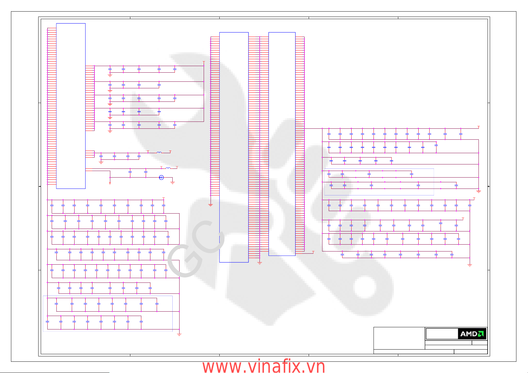
RV770 GL A11
RV770 GL A11
C221
C221
1uF_6.3V
1uF_6.3V
C231
C231
1uF_6.3V
1uF_6.3V
C241
C241
1uF_6.3V
1uF_6.3V
C262
C262
1uF_6.3V
1uF_6.3V
5
C252
C252
1uF_6.3V
1uF_6.3V
AA17
AB17
AD17
AE17
AF17
AH17
AJ17
AK17
AR17
AT17
AU17
AU18
AU19
U17
U19
U21
U22
U24
U25
U26
U28
U29
U30
U35
U36
U37
V37
W37
W17
AA37
AV22
AU21
AV21
AV19
AT37
AT38
C222
C222
1uF_6.3V
1uF_6.3V
C242
C242
1uF_6.3V
1uF_6.3V
C263
C263
1uF_6.3V
1uF_6.3V
C232
C232
1uF_6.3V
1uF_6.3V
C253
C253
1uF_6.3V
1uF_6.3V
C243
C243
1uF_6.3V
1uF_6.3V
C264
C264
1uF_6.3V
1uF_6.3V
C186
C186
100nF_6.3V
100nF_6.3V
GND_SPVDD
C223
C223
1uF_6.3V
1uF_6.3V
C233
C233
1uF_6.3V
1uF_6.3V
C254
C254
1uF_6.3V
1uF_6.3V
C265
C265
1uF_6.3V
1uF_6.3V
C343
C343
1uF_6.3V
1uF_6.3V
C353
C353
1uF_6.3V
1uF_6.3V
C354
C354
1uF_6.3V
1uF_6.3V
C349
C349
1uF_6.3V
1uF_6.3V
C361
C361
1uF_6.3V
1uF_6.3V
C244
C244
1uF_6.3V
1uF_6.3V
C187
C187
100nF_6.3V
100nF_6.3V
C224
C224
1uF_6.3V
1uF_6.3V
C234
C234
1uF_6.3V
1uF_6.3V
C255
C255
1uF_6.3V
1uF_6.3V
C266
C266
1uF_6.3V
1uF_6.3V
C344
C344
1uF_6.3V
1uF_6.3V
C352
C352
1uF_6.3V
1uF_6.3V
C355
C355
1uF_6.3V
1uF_6.3V
C357
C357
1uF_6.3V
1uF_6.3V
C350
C350
1uF_6.3V
1uF_6.3V
C245
C245
1uF_6.3V
1uF_6.3V
C188
C188
1uF_6.3V
1uF_6.3V
C363
C363
1uF_6.3V
1uF_6.3V
C225
C225
1uF_6.3V
1uF_6.3V
C256
C256
1uF_6.3V
1uF_6.3V
C267
C267
1uF_6.3V
1uF_6.3V
C235
C235
1uF_6.3V
1uF_6.3V
C246
C246
1uF_6.3V
1uF_6.3V
C345
C345
1uF_6.3V
1uF_6.3V
C347
C347
1uF_6.3V
1uF_6.3V
C346
C346
1uF_6.3V
1uF_6.3V
C359
C359
1uF_6.3V
1uF_6.3V
C362
C362
1uF_6.3V
1uF_6.3V
C189
C189
1uF_6.3V
1uF_6.3V
C226
C226
1uF_6.3V
1uF_6.3V
C257
C257
1uF_6.3V
1uF_6.3V
C268
C268
1uF_6.3V
1uF_6.3V
C364
C364
100nF_6.3V
100nF_6.3V
C236
C236
1uF_6.3V
1uF_6.3V
C247
C247
1uF_6.3V
1uF_6.3V
BLM15BD121SN1
BLM15BD121SN1
C227
C227
1uF_6.3V
1uF_6.3V
C258
C258
1uF_6.3V
1uF_6.3V
U1G
U1G
AA12
VDDR1#1
AB9
VDDR1#2
AD12
VDDR1#3
AE9
VDDR1#4
AE15
VDDR1#5
AB15
VDDR1#6
AH9
VDDR1#7
AH15
VDDR1#8
AJ12
VDDR1#9
AK15
VDDR1#10
AK9
VDDR1#11
AM12
VDDR1#12
AN15
VDDR1#13
AN9
VDDR1#14
AR12
VDDR1#15
AT15
D D
VDDR1#16
AT9
VDDR1#17
AU12
VDDR1#18
AW9
VDDR1#19
AW14
VDDR1#20
BB14
VDDR1#21
BE18
VDDR1#22
BC10
VDDR1#23
AW18
VDDR1#24
BE11
VDDR1#25
BE15
VDDR1#26
BB17
VDDR1#27
K11
VDDR1#28
J14
VDDR1#29
J17
VDDR1#30
J30
VDDR1#31
J33
VDDR1#32
J36
VDDR1#33
J19
VDDR1#34
J22
VDDR1#35
J25
VDDR1#36
J28
VDDR1#37
J39
VDDR1#38
K43
VDDR1#39
L45
VDDR1#40
L10
VDDR1#41
L15
VDDR1#42
M18
VDDR1#43
M21
VDDR1#44
M24
VDDR1#45
R22
VDDR1#46
M29
VDDR1#47
M32
VDDR1#48
M35
VDDR1#49
M37
VDDR1#50
P14
VDDR1#51
P17
VDDR1#52
R19
VDDR1#53
C C
R25
VDDR1#54
R28
VDDR1#55
R30
VDDR1#56
R33
VDDR1#57
R36
VDDR1#58
P39
VDDR1#59
P42
VDDR1#60
P9
VDDR1#61
R11
VDDR1#62
R45
VDDR1#63
U14
VDDR1#64
U42
VDDR1#65
U9
VDDR1#66
V12
VDDR1#67
V39
VDDR1#68
V45
VDDR1#69
W9
VDDR1#70
W15
VDDR1#71
C220
C220
C219
C219
1uF_6.3V
1uF_6.3V
1uF_6.3V
1uF_6.3V
C229
C229
1uF_6.3V
1uF_6.3V
B B
C239
C239
C240
C240
1uF_6.3V
1uF_6.3V
1uF_6.3V
1uF_6.3V
C250
C250
1uF_6.3V
1uF_6.3V
C260
C260
C261
C261
1uF_6.3V
1uF_6.3V
1uF_6.3V
1uF_6.3V
4
C348
C348
10uF_6.3V
10uF_6.3V
C360
C360
10uF_6.3V
10uF_6.3V
C356
C356
10uF_6.3V
10uF_6.3V
C358
C358
10uF_6.3V
10uF_6.3V
C351
C351
10uF_6.3V
10uF_6.3V
B112
B112
+1.8V+VDD_CT
B122
B122
+SPVDD +VDDC
BLM15BD121SN1
BLM15BD121SN1
12
NS_VIA
NS_VIA
NS7
NS7
+MVDDQ
C228
C228
1uF_6.3V
1uF_6.3V
C237
C237
C238
C238
1uF_6.3V
1uF_6.3V
1uF_6.3V
1uF_6.3V
C248
C248
C249
C249
1uF_6.3V
1uF_6.3V
1uF_6.3V
1uF_6.3V
C259
C259
1uF_6.3V
1uF_6.3V
C270
C270
C269
C269
1uF_6.3V
1uF_6.3V
1uF_6.3V
1uF_6.3V
C374
C374
10uF_6.3V
10uF_6.3V
C375
C375
10uF_6.3V
10uF_6.3V
C376
C376
10uF_6.3V
10uF_6.3V
+VDDC
3
U1I
G39
VSSM#101
G41
VSSM#102
G43
VSSM#103
G45
VSSM#104
G9
VSSM#105
H1
VSSM#106
J47
VSSM#107
H53
VSSM#108
J7
VSSM#109
J11
VSSM#110
K2
VSSM#111
L40
VSSM#112
K14
VSSM#113
K17
VSSM#114
K19
VSSM#115
K22
VSSM#116
K25
VSSM#117
K28
VSSM#118
K30
VSSM#119
K33
VSSM#120
K36
VSSM#121
K39
VSSM#122
L47
VSSM#123
K52
VSSM#124
L7
VSSM#125
P2
VSSM#126
M2
VSSM#127
M43
VSSM#128
M52
VSSM#129
L9
VSSM#130
R15
VSSM#131
N18
VSSM#132
N21
VSSM#133
N24
VSSM#134
N26
VSSM#135
N29
VSSM#136
N32
VSSM#137
N35
VSSM#138
N37
VSSM#139
N40
VSSM#140
N47
VSSM#141
N7
VSSM#142
P10
VSSM#143
P41
VSSM#144
R53
VSSM#145
R12
VSSM#146
M15
VSSM#147
R17
VSSM#148
T19
VSSM#149
T22
VSSM#150
T25
VSSM#151
T28
VSSM#152
T30
VSSM#153
T33
VSSM#154
T36
VSSM#155
R44
VSSM#156
R47
VSSM#157
R7
VSSM#158
T2
VSSM#159
T48
VSSM#160
U10
VSSM#161
U15
VSSM#162
U41
VSSM#163
U7
VSSM#164
V13
VSSM#165
V38
VSSM#166
V44
VSSM#167
V2
VSSM#168
W10
VSSM#169
W16
VSSM#170
W7
VSSM#171
Y2
VSSM#172
U1I
B14
B18
B22
A39
A49
A5
AA13
AA7
AB10
AB16
AB2
AC7
AD13
AD2
AE10
AE16
AE7
AF13
AF2
AG7
AH10
AH16
AH2
AJ13
AJ7
AK10
AK16
AK2
AL7
AM13
AM2
AN1
AN10
AN16
AN7
AR13
AR7
AT10
AT16
AT2
AU13
AU7
AW1
AW10
AW7
AY13
AY2
B10
B16
B26
B30
A33
B42
BA14
BA17
BA7
AY11
AV18
BB2
BD15
BD18
BC7
BC12
BD2
BE7
BG11
BG13
BG15
BG9
BJ1
BM12
BN8
BN15
BM10
BN5
B12
B20
B24
B28
B32
B36
B40
B44
A8
E1
E53
G11
G13
G15
G17
G19
G21
G23
G25
G27
G29
G31
G33
G35
G37
AA20
VSSC#1
AA23
VSSC#2
AA25
VSSC#3
AA28
VSSC#4
AA30
VSSC#5
AA33
VSSC#6
AA35
VSSC#7
AC19
VSSC#8
AC21
VSSC#9
AC24
VSSC#10
AC26
VSSC#11
AC29
VSSC#12
AC31
VSSC#13
AC34
VSSC#14
AD20
VSSC#15
AD23
VSSC#16
AD25
VSSC#17
AD28
VSSC#18
AD30
VSSC#19
AD33
VSSC#20
AD35
VSSC#21
AE19
VSSC#22
AE21
VSSC#23
AE24
VSSC#24
AE26
VSSC#25
AE29
VSSC#26
AE31
VSSC#27
AE34
VSSC#28
AF20
VSSC#29
AF23
VSSC#30
AF25
VSSC#31
AF28
VSSC#32
AF30
VSSC#33
AF33
VSSC#34
AF35
VSSC#35
AH19
VSSC#36
AH21
VSSC#37
AH24
VSSC#38
AH26
VSSC#39
AH29
VSSC#40
AH31
VSSC#41
AH34
VSSC#42
AJ20
VSSC#43
AJ23
VSSC#44
AJ25
VSSC#45
AJ28
VSSC#46
AJ30
VSSC#47
AJ33
VSSC#48
AJ35
VSSC#49
AK19
VSSC#50
AK21
VSSC#51
AK24
VSSC#52
AK26
VSSC#53
AK29
VSSC#54
AK31
VSSC#55
AK34
VSSC#56
AL20
VSSC#57
AL23
VSSC#58
AL25
VSSC#59
AL28
VSSC#60
AL30
VSSC#61
AL33
VSSC#62
AL35
VSSC#63
AN19
VSSC#64
AN21
VSSC#65
AN24
VSSC#66
AN26
VSSC#67
AN29
VSSC#68
AN31
VSSC#69
AN34
VSSC#70
AP20
VSSC#71
AP23
VSSC#72
密
AP25
VSSC#73
AP28
VSSC#74
AP30
VSSC#75
AP33
VSSC#76
AR21
VSSC#77
AR24
VSSC#78
AR26
VSSC#79
AR29
VSSC#80
AR31
VSSC#81
AR34
VSSC#82
W20
VSSC#83
W23
VSSC#84
W25
VSSC#85
W28
VSSC#86
W30
VSSC#87
W33
VSSC#88
W35
VSSC#89
Y19
VSSC#90
Y21
VSSC#91
Y24
VSSC#92
Y26
VSSC#93
Y29
VSSC#94
Y31
VSSC#95
Y34
VSSC#96
AP35
VSSC#97
VSSM#1
VSSM#2
VSSM#3
VSSM#4
VSSM#5
VSSM#6
VSSM#7
VSSM#8
VSSM#9
VSSM#10
VSSM#11
VSSM#12
VSSM#13
VSSM#14
VSSM#15
VSSM#16
VSSM#17
VSSM#18
VSSM#19
VSSM#20
VSSM#21
VSSM#22
VSSM#23
VSSM#24
VSSM#25
VSSM#26
VSSM#27
VSSM#28
VSSM#29
VSSM#30
VSSM#31
VSSM#32
VSSM#33
VSSM#34
VSSM#35
VSSM#36
VSSM#37
VSSM#38
VSSM#39
VSSM#40
VSSM#41
VSSM#42
VSSM#43
VSSM#44
VSSM#45
VSSM#46
VSSM#47
VSSM#48
VSSM#49
VSSM#50
VSSM#51
VSSM#52
VSSM#53
VSSM#54
VSSM#55
VSSM#56
VSSM#57
VSSM#58
VSSM#59
VSSM#60
VSSM#61
VSSM#62
VSSM#63
VSSM#64
VSSM#65
VSSM#66
VSSM#67
VSSM#68
VSSM#69
VSSM#70
VSSM#71
VSSM#72
VSSM#73
VSSM#74
VSSM#75
VSSM#76
VSSM#77
VSSM#78
VSSM#79
VSSM#80
VSSM#81
VSSM#82
VSSM#83
VSSM#84
VSSM#85
VSSM#86
機
VSSM#87
VSSM#88
VSSM#89
VSSM#90
VSSM#91
VSSM#92
VSSM#93
VSSM#94
VSSM#95
VSSM#96
VSSM#97
VSSM#98
VSSM#99
VSSM#100
RV770 GL A11
RV770 GL A11
VDDC#1
VDDC#2
VDDC#3
VDDC#4
VDDC#5
VDDC#6
VDDC#7
VDDC#8
VDDC#9
VDDC#10
VDDC#11
VDDC#12
VDDC#13
VDDC#14
VDDC#15
VDDC#16
VDDC#17
VDDC#18
VDDC#19
VDDC#20
VDDC#21
VDDC#22
VDDC#23
VDDC#24
VDDC#25
VDDC#26
VDDC#27
VDDC#28
VDDC#29
VDDC#30
VDDC#31
VDDC#32
VDDC#33
VDDC#34
VDDC#35
VDDC#36
VDDC#37
VDDC#38
VDDC#39
VDDC#40
VDDC#41
VDDC#42
VDDC#43
VDDC#44
VDDC#45
VDDC#46
VDDC#47
VDDC#48
VDDC#49
VDDC#50
VDDC#51
VDDC#52
VDDC#53
VDDC#54
VDDC#55
VDDC#56
VDDC#57
VDDC#58
VDDC#59
VDDC#60
VDDC#61
VDDC#62
VDDC#63
VDDC#64
VDDC#65
VDDC#66
VDDC#67
VDDC#68
VDDC#69
VDDC#70
VDDC#71
VDDC#72
VDDC#73
VDDC#74
VDDC#75
VDDC#76
VDDC#77
VDDC#78
VDDC#79
VDDC#80
VDDC#81
VDDC#82
VDDC#83
VDDC#84
VDDC#85
VDDC#86
VDDC#87
VDDC#88
VDDC#89
VDDC#90
VDDC#91
VDDC#92
VDDC#93
VDDC#94
VDDC#95
VDDC#96
VDDC#97
SP_PVDD
RV770 GL A11
RV770 GL A11
U1H
U1H
AA19
AA21
AA24
AA26
AA29
AA31
AA34
AC20
AC23
AC25
AC28
AC30
AC33
AC35
AD19
AD21
AD24
AD26
AD29
AD31
AD34
AE20
AE23
AE25
AE28
AE30
AE33
AE35
AF19
AF21
AF24
AF26
AF29
AF31
AF34
AH20
AH23
AH25
AH28
AH30
AH33
AH35
AJ19
AJ21
AJ24
AJ26
AJ29
AJ31
AJ34
AK20
AK23
AK25
AK28
AK30
AK33
AK35
AL19
AL21
文件
AL24
AL26
AL29
AL31
AL34
AN20
AN23
AN25
AN28
AN30
AN33
AN35
AP21
AP24
AP26
AP29
AP31
AP34
AR20
AR23
AR25
AR28
AR30
AR33
W19
W21
W24
W26
W29
W31
W34
Y20
Y23
Y25
Y28
Y30
Y33
Y35
+PCIE_PVDD
AR35
AR38
C152
C152
1uF_6.3V
1uF_6.3V
C164
C164
1uF_6.3V
1uF_6.3V
C174
C174
1uF_6.3V
1uF_6.3V
C179
C179
10uF_X6S
10uF_X6S
MC179
MC179
NC_4.7uF_6.3V
NC_4.7uF_6.3V
C377
C377
1uF_6.3V
1uF_6.3V
C190
C190
1uF_6.3V
1uF_6.3V
C200
C200
1uF_6.3V
1uF_6.3V
C153
C153
1uF_6.3V
1uF_6.3V
C165
C165
1uF_6.3V
1uF_6.3V
C175
C175
1uF_6.3V
1uF_6.3V
C180
C180
10uF_X6S
10uF_X6S
MC180
MC180
NC_4.7uF_6.3V
NC_4.7uF_6.3V
C378
C378
1uF_6.3V
1uF_6.3V
C191
C191
1uF_6.3V
1uF_6.3V
C201
C201
1uF_6.3V
1uF_6.3V
C211
C211
100nF_6.3V
100nF_6.3V
2
C154
C154
1uF_6.3V
1uF_6.3V
C166
C166
1uF_6.3V
1uF_6.3V
C379
C379
1uF_6.3V
1uF_6.3V
C192
C192
1uF_6.3V
1uF_6.3V
C202
C202
1uF_6.3V
1uF_6.3V
C155
C155
1uF_6.3V
1uF_6.3V
C167
C167
1uF_6.3V
1uF_6.3V
C176
C176
1uF_6.3V
1uF_6.3V
C203
C203
1uF_6.3V
1uF_6.3V
C212
C212
100nF_6.3V
100nF_6.3V
C380
C380
1uF_6.3V
1uF_6.3V
C193
C193
1uF_6.3V
1uF_6.3V
C156
C156
C157
C157
1uF_6.3V
1uF_6.3V
1uF_6.3V
1uF_6.3V
C168
C168
C169
C169
1uF_6.3V
1uF_6.3V
1uF_6.3V
1uF_6.3V
C177
C177
1uF_6.3V
1uF_6.3V
C182
C182
10uF_X6S
10uF_X6S
MC182
MC182
NC_4.7uF_6.3V
NC_4.7uF_6.3V
Overlapped Footprints
C381
C381
1uF_6.3V
1uF_6.3V
C194
C194
1uF_6.3V
1uF_6.3V
C204
C204
C205
C205
1uF_6.3V
1uF_6.3V
1uF_6.3V
1uF_6.3V
C213
C213
C214
C214
100nF_6.3V
100nF_6.3V
100nF_6.3V
100nF_6.3V
C178
C178
1uF_6.3V
1uF_6.3V
C382
C382
1uF_6.3V
1uF_6.3V
C195
C195
1uF_6.3V
1uF_6.3V
C158
C158
1uF_6.3V
1uF_6.3V
C170
C170
1uF_6.3V
1uF_6.3V
C383
C383
1uF_6.3V
1uF_6.3V
C209
C209
1uF_6.3V
1uF_6.3V
C215
C215
100nF_6.3V
100nF_6.3V
C159
C159
1uF_6.3V
1uF_6.3V
C171
C171
1uF_6.3V
1uF_6.3V
C196
C196
1uF_6.3V
1uF_6.3V
C185
C185
10uF_X6S
10uF_X6S
C160
C160
1uF_6.3V
1uF_6.3V
C172
C172
1uF_6.3V
1uF_6.3V
MC185
MC185
4.7uF_6.3V
4.7uF_6.3V
C384
C384
1uF_6.3V
1uF_6.3V
C197
C197
1uF_6.3V
1uF_6.3V
C206
C206
1uF_6.3V
1uF_6.3V
C216
C216
100nF_6.3V
100nF_6.3V
C161
C161
1uF_6.3V
1uF_6.3V
C385
C385
1uF_6.3V
1uF_6.3V
C207
C207
1uF_6.3V
1uF_6.3V
1
C173
C173
1uF_6.3V
1uF_6.3V
C198
C198
1uF_6.3V
1uF_6.3V
C217
C217
100nF_6.3V
100nF_6.3V
C162
C162
1uF_6.3V
1uF_6.3V
C386
C386
1uF_6.3V
1uF_6.3V
C208
C208
1uF_6.3V
1uF_6.3V
MC132
MC132
NC_4.7uF_6.3V
NC_4.7uF_6.3V
C387
C387
1uF_6.3V
1uF_6.3V
C199
C199
1uF_6.3V
1uF_6.3V
C218
C218
100nF_6.3V
100nF_6.3V
C163
C163
1uF_6.3V
1uF_6.3V
+VDDC
C210
C210
1uF_6.3V
1uF_6.3V
+VDDC
C388
C388
1uF_6.3V
1uF_6.3V
+VDDC
C272
C272
C271
C271
100nF_6.3V
100nF_6.3V
100nF_6.3V
100nF_6.3V
MC285
MC285
MC286
MC286
NC_4.7uF_6.3V
NC_4.7uF_6.3V
NC_4.7uF_6.3V
C286
C286
10uF_X6S
10uF_X6S
NC_4.7uF_6.3V
A A
C285
C285
10uF_X6S
10uF_X6S
C287
C287
10uF_X6S
10uF_X6S
C273
C273
100nF_6.3V
100nF_6.3V
MC287
MC287
NC_4.7uF_6.3V
NC_4.7uF_6.3V
5
C274
C274
100nF_6.3V
100nF_6.3V
C288
C288
10uF_X6S
10uF_X6S
MC288
MC288
NC_4.7uF_6.3V
NC_4.7uF_6.3V
C289
C289
10uF_X6S
10uF_X6S
C275
C275
100nF_6.3V
100nF_6.3V
MC289
MC289
NC_4.7uF_6.3V
NC_4.7uF_6.3V
C290
C290
10uF_X6S
10uF_X6S
C276
C276
100nF_6.3V
100nF_6.3V
MC290
MC290
NC_4.7uF_6.3V
NC_4.7uF_6.3V
C291
C291
10uF_X6S
10uF_X6S
C277
C277
C278
C278
100nF_6.3V
100nF_6.3V
100nF_6.3V
100nF_6.3V
MC291
MC291
NC_4.7uF_6.3V
NC_4.7uF_6.3V
Overlapped Footprints
C292
C292
10uF_X6S
10uF_X6S
MC292
MC292
NC_4.7uF_6.3V
NC_4.7uF_6.3V
4
Printed with FinePrint - purchase at www.fineprint.com
3
www.vinafix.vn
CONFIDENTIAL & PROPRIETARY TO ADVANCED MICRO DEVICES INC.
CONFIDENTIAL & PROPRIETARY TO ADVANCED MICRO DEVICES INC.
CONFIDENTIAL & PROPRIETARY TO ADVANCED MICRO DEVICES INC.
?2007 Advanced Micro D evices
?2007 Advanced Micro D evices
?2007 Advanced Micro D evices
This AMD Board schemat ic and desi gn is the exclu sive pr opert y o f AMD,
This AMD Board schemat ic and desi gn is the exclu sive pr opert y o f AMD,
This AMD Board schemat ic and desi gn is the exclu sive pr opert y o f AMD,
and is provided only to entiti es under a non -disclosure agreement
and is provided only to entiti es under a non -disclosure agreement
and is provided only to entiti es under a non -disclosure agreement
with AMD for evalu ation purposes. F urther distribut ion or di sclosure
with AMD for evalu ation purposes. F urther distribut ion or di sclosure
with AMD for evalu ation purposes. F urther distribut ion or di sclosure
is strictly prohibited. Use of th is sch ematic and de sign fo r any pu rpose
is strictly prohibited. Use of th is sch ematic and de sign fo r any pu rpose
is strictly prohibited. Use of th is sch ematic and de sign fo r any pu rpose
other than evaluation re quires a Board T echnology License Agre ement
other than evaluation re quires a Board T echnology License Agre ement
other than evaluation re quires a Board T echnology License Agre ement
with AMD. AMD makes no r epre sentat ions or war ranties of an y kind
with AMD. AMD makes no r epre sentat ions or war ranties of an y kind
with AMD. AMD makes no r epre sentat ions or war ranties of an y kind
regarding this schemat ic and design , in cluding, n ot limit ed to,
regarding this schemat ic and design , in cluding, n ot limit ed to,
regarding this schemat ic and design , in cluding, n ot limit ed to,
any implied warranty of mer chanti bility or fitness for a par ticular
any implied warranty of mer chanti bility or fitness for a par ticular
any implied warranty of mer chanti bility or fitness for a par ticular
purpose, and disclaims respons ibility forany co nsequences resul ting
purpose, and disclaims respons ibility forany co nsequences resul ting
purpose, and disclaims respons ibility forany co nsequences resul ting
from use of the information include d herein .
from use of the information include d herein .
from use of the information include d herein .
Title
Title
Title
RH RV770 GDDR5 DVI-I VO DVI-I FH
RH RV770 GDDR5 DVI-I VO DVI-I FH
2
RH RV770 GDDR5 DVI-I VO DVI-I FH
Advanced Micro Devices Inc.
Advanced Micro Devices Inc.
Advanced Micro Devices Inc.
1 Commerce Valley Drive East
1 Commerce Valley Drive East
1 Commerce Valley Drive East
Markham, Ontario
Markham, Ontario
Markham, Ontario
Thursday, October 09, 2008
Thursday, October 09, 2008
Thursday, October 09, 2008
Sheet
Sheet
Sheet
422
422
422
of
of
of
1
Doc No.
Doc No.
Doc No.
RevDate:
RevDate:
RevDate:
1
1
1
105-B507xx-10
105-B507xx-10
105-B507xx-10
Page 5
5
U1C
C181
C181
1uF_6.3V
1uF_6.3V
AW19
V40
R42
V41
R41
V42
V43
U45
P44
M48
M50
L53
L51
P48
P50
P52
N53
L49
J51
K50
K48
G52
H48
F48
C51
C43
F44
E43
D44
A46
D46
F46
B47
L44
M45
P40
M44
R43
P43
J43
K44
M42
K45
R51
R49
E50
D49
U44
N49
J49
C45
U43
N51
H50
E45
U38
R39
R40
J44
P45
L43
U40
U39
U33
U32
T32
P36
+MVDDQ
+MVDDQ
U1C
DQA0_0
DQA0_1
DQA0_2
DQA0_3
DQA0_4
DQA0_5
DQA0_6
DQA0_7
DQA0_8
DQA0_9
DQA0_10
DQA0_11
DQA0_12
DQA0_13
DQA0_14
DQA0_15
DQA0_16
DQA0_17
DQA0_18
DQA0_19
DQA0_20
DQA0_21
DQA0_22
DQA0_23
DQA0_24
DQA0_25
DQA0_26
DQA0_27
DQA0_28
DQA0_29
DQA0_30
DQA0_31
MAA0_0
MAA0_1
MAA0_2
MAA0_3
MAA0_4
MAA0_5
MAA0_6
MAA0_7
MAA0_8
ADBIA0
WCKA0_0
WCKA0B_0
WCKA0_1
WCKA0B_1
EDCA0_0
EDCA0_1
EDCA0_2
EDCA0_3
DDBIA0_0
DDBIA0_1
DDBIA0_2
DDBIA0_3
WEA0B
CSA0B_0
CSA0B_1
CASA0B
RASA0B
CKEA0
CLKA0
CLKA0B
MVREFAS
MVREFAD
MEM_CALRPA
MEM_CALRNA
DRAM_RST
RV770 GL A11
RV770 GL A11
R122
R122
40.2R
40.2R
1%
R125
100R
100R
1%
R126
R126
40.2R
40.2R
1%
R128
R128
100R
100R
1%
DNI
C293
C293
NC_1uF_6.3V
NC_1uF_6.3V
C300
C300
1uF_6.3V
1uF_6.3V
C303
C303
NC_1uF_6.3V
NC_1uF_6.3V
C305
C305
1uF_6.3V
1uF_6.3V
DQA1_0
DQA1_1
DQA1_2
DQA1_3
DQA1_4
DQA1_5
DQA1_6
DQA1_7
DQA1_8
DQA1_9
DQA1_10
DQA1_11
DQA1_12
DQA1_13
DQA1_14
DQA1_15
DQA1_16
DQA1_17
DQA1_18
DQA1_19
DQA1_20
DQA1_21
DQA1_22
DQA1_23
DQA1_24
DQA1_25
DQA1_26
DQA1_27
DQA1_28
DQA1_29
DQA1_30
DQA1_31
MAA1_0
MAA1_1
MAA1_2
MAA1_3
MAA1_4
MAA1_5
MAA1_6
MAA1_7
MAA1_8
ADBIA1
WCKA1_0
WCKA1B_0
WCKA1_1
WCKA1B_1
EDCA1_0
EDCA1_1
EDCA1_2
EDCA1_3
DDBIA1_0
DDBIA1_1
DDBIA1_2
DDBIA1_3
WEA1B
CSA1B_0
CSA1B_1
CASA1B
RASA1B
CKEA1
CLKA1
CLKA1B
MPVDD#0
MPVDD#1
MPVDD#2
DNI
DQA0_[31..0](8)
D D
MAA0_[8..0](8)
ADBIA0(8)
WCKA0_0(8)
WCKA0b_0(8)
WCKA0_1(8)
C C
B B
WCKA0b_1(8)
EDCA0_0(8)
EDCA0_1(8)
EDCA0_2(8)
EDCA0_3(8)
DDBIA0_0(8)
DDBIA0_1(8)
DDBIA0_2(8)
DDBIA0_3(8)
DRAM_RST(8,9)
DQA0_0
DQA0_1
DQA0_2
DQA0_3
DQA0_4
DQA0_5
DQA0_6
DQA0_7
DQA0_8
DQA0_9
DQA0_10
DQA0_11
DQA0_12
DQA0_13
DQA0_14
DQA0_15
DQA0_16
DQA0_17
DQA0_18
DQA0_19
DQA0_20
DQA0_21
DQA0_22
DQA0_23
DQA0_24
DQA0_25
DQA0_26
DQA0_27
DQA0_28
DQA0_29
DQA0_30
DQA0_31
MAA0_0
MAA0_1
MAA0_2
MAA0_3
MAA0_4
MAA0_5
MAA0_6
MAA0_7
MAA0_8
WEA0b(8)
CSA0b_0(8)
CASA0b(8)
RASA0b(8)
CKEA0(8)
CLKA0(8)
CLKA0b(8)
MVREFS_A
MVREFD_A
+MVDDQ
R120 243RR120 243R
R121 243RR121 243R C336
R102
R102
10K
10K
D30
A31
F30
E29
D32
C33
E33
F32
J35
L32
L35
K35
M30
L33
L30
J29
F34
A35
E35
C35
E37
C37
B38
A37
F42
E41
A43
D42
D40
E39
C39
F40
J42
K40
L37
J40
J37
K37
M39
M40
K42
L42
B34
D34
D38
F38
C31
J32
D36
C41
E31
K32
F36
A41
N36
P37
R37
N39
L39
T37
M36
L36
J10
K10
K9
MVREFD_A
MVREFD/S =0.7*
VDDR1
(GDDR3/4/5)
MVREFS_A
4
DQA1_10
DQA1_11
DQA1_12
DQA1_13
DQA1_14
DQA1_15
DQA1_16
DQA1_17
DQA1_18
DQA1_19
DQA1_20
DQA1_21
DQA1_22
DQA1_23
DQA1_24
DQA1_25
DQA1_26
DQA1_27
DQA1_28
DQA1_29
DQA1_30
DQA1_31
DQA1_0
DQA1_1
DQA1_2
DQA1_3
DQA1_4
DQA1_5
DQA1_6
DQA1_7
DQA1_8
DQA1_9
MAA1_0
MAA1_1
MAA1_2
MAA1_3
MAA1_4
MAA1_5
MAA1_6
MAA1_7
MAA1_8
1uF_6.3V
1uF_6.3V
3
DQA1_[31..0] (8)
MAA1_[8..0] (8)
ADBIA1 (8)
WCKA1_0 (8)
WCKA1b_0 (8)
WCKA1_1 (8)
WCKA1b_1 (8)
EDCA1_0 (8)
EDCA1_1 (8)
EDCA1_2 (8)
EDCA1_3 (8)
DDBIA1_0 (8)
DDBIA1_1 (8)
DDBIA1_2 (8)
DDBIA1_3 (8)
WEA1b (8)
CSA1b_0 (8)
CASA1b (8)
RASA1b (8)
CKEA1 (8)
CLKA1 (8)
CLKA1b (8)
+1.8V+MPVDD
B114
B114
10R_1A_0402
10R_1A_0402
1uF_6.3V
1uF_6.3V
C336
C337
C337
10uF_X6S
10uF_X6S
C338
C338
C339
C339
100nF_6.3V
100nF_6.3V
DQB0_[31..0](8)
MAB0_[8..0](8)
ADBIB0(8)
WCKB0_0(8)
WCKB0b_0(8)
WCKB0_1(8)
WCKB0b_1(8)
EDCB0_0(8)
EDCB0_1(8)
EDCB0_2(8)
EDCB0_3(8)
DDBIB0_1(8)
DDBIB0_0(8)
DDBIB0_2(8)
DDBIB0_3(8)
密
DQB0_0
DQB0_1
DQB0_2
DQB0_3
DQB0_4
DQB0_5
DQB0_6
DQB0_7
DQB0_8
DQB0_9
DQB0_10
DQB0_11
DQB0_12
DQB0_13
DQB0_14
DQB0_15
DQB0_16
DQB0_17
DQB0_18
DQB0_19
DQB0_20
DQB0_21
DQB0_22
DQB0_23
DQB0_24
DQB0_25
DQB0_26
DQB0_27
DQB0_28
DQB0_29
DQB0_30
DQB0_31
MAB0_0
MAB0_1
MAB0_2
MAB0_3
MAB0_4
MAB0_5
MAB0_6
MAB0_7
MAB0_8
文件
WEB0b(8)
CSB0b_0(8)
CASB0b(8)
RASB0b(8)
CKEB0(8)
CLKB0(8)
CLKB0b(8)
+MVDDQ
R118 243RR118 243R
R119 243RR119 243R
MVREFS_B
MVREFD_B
P35
P32
T35
P33
N30
P30
R32
R35
M25
M28
N25
T26
K26
J26
R29
N28
A29
C29
F28
D28
A27
D26
E25
F26
E21
D22
C21
A21
C23
E23
F24
D24
J24
L24
L25
P24
L28
P25
N22
P22
L22
M22
K29
L29
C25
A25
N33
L26
E27
F22
M33
M26
C27
A23
T29
P26
R26
R24
K24
T24
P29
P28
T17
U18
T21
R21
機
U1D
U1D
DQB0_0
DQB0_1
DQB0_2
DQB0_3
DQB0_4
DQB0_5
DQB0_6
DQB0_7
DQB0_8
DQB0_9
DQB0_10
DQB0_11
DQB0_12
DQB0_13
DQB0_14
DQB0_15
DQB0_16
DQB0_17
DQB0_18
DQB0_19
DQB0_20
DQB0_21
DQB0_22
DQB0_23
DQB0_24
DQB0_25
DQB0_26
DQB0_27
DQB0_28
DQB0_29
DQB0_30
DQB0_31
MAB0_0
MAB0_1
MAB0_2
MAB0_3
MAB0_4
MAB0_5
MAB0_6
MAB0_7
MAB0_8
ADBIB0
WCKB0_0
WCKB0B_0
WCKB0_1
WCKB0B_1
EDCB0_0
EDCB0_1
EDCB0_2
EDCB0_3
DDBIB0_0
DDBIB0_1
DDBIB0_2
DDBIB0_3
WEB0B
CSB0B_0
CSB0B_1
CASB0B
RASB0B
CKEB0
CLKB0
CLKB0B
MVREFBS
MVREFBD
MEM_CALRPB
MEM_CALRNB
RV770 GL A11
RV770 GL A11
+MVDDQ
R123
R123
40.2R
40.2R
1%
R124
R124
100R
100RR125
1%
+MVDDQ
R127
R127
40.2R
40.2R
1%
R129
R129
100R
100R
1%
2
DQB1_0
DQB1_1
DQB1_2
DQB1_3
DQB1_4
DQB1_5
DQB1_6
DQB1_7
DQB1_8
DQB1_9
DQB1_10
DQB1_11
DQB1_12
DQB1_13
DQB1_14
DQB1_15
DQB1_16
DQB1_17
DQB1_18
DQB1_19
DQB1_20
DQB1_21
DQB1_22
DQB1_23
DQB1_24
DQB1_25
DQB1_26
DQB1_27
DQB1_28
DQB1_29
DQB1_30
DQB1_31
MAB1_0
MAB1_1
MAB1_2
MAB1_3
MAB1_4
MAB1_5
MAB1_6
MAB1_7
MAB1_8
ADBIB1
WCKB1_0
WCKB1B_0
WCKB1_1
WCKB1B_1
EDCB1_0
EDCB1_1
EDCB1_2
EDCB1_3
DDBIB1_0
DDBIB1_1
DDBIB1_2
DDBIB1_3
WEB1B
CSB1B_0
CSB1B_1
CASB1B
RASB1B
CLKB1B
C295
C295
DNI
NC_1uF_6.3V
NC_1uF_6.3V
C298
C298
1uF_6.3V
1uF_6.3V
C301
C301
NC_1uF_6.3V
NC_1uF_6.3V
C307
C307
1uF_6.3V
1uF_6.3V
CKEB1
CLKB1
DNI
C3
D5
B7
D8
E9
F10
D10
A11
K18
L18
L17
M17
M12
L12
K12
J12
F12
D12
C13
A13
F14
C15
A15
E15
F20
C17
D20
C19
E19
D18
E17
A17
J18
M19
P18
T18
N17
R18
N19
P21
L19
J21
C11
E11
D16
F16
F8
K15
E13
A19
C9
J15
D14
F18
P15
N15
L14
K21
P19
L21
N14
M14
MVREFD_B
MVREFS_B
DQB1_0
DQB1_1
DQB1_2
DQB1_3
DQB1_4
DQB1_5
DQB1_6
DQB1_7
DQB1_8
DQB1_9
DQB1_10
DQB1_11
DQB1_12
DQB1_13
DQB1_14
DQB1_15
DQB1_16
DQB1_17
DQB1_18
DQB1_19
DQB1_20
DQB1_21
DQB1_22
DQB1_23
DQB1_24
DQB1_25
DQB1_26
DQB1_27
DQB1_28
DQB1_29
DQB1_30
DQB1_31
MAB1_0
MAB1_1
MAB1_2
MAB1_3
MAB1_4
MAB1_5
MAB1_6
MAB1_7
MAB1_8
MVREFD/S =0.7*
VDDR1
(GDDR3/4/5)
DQB1_[31..0] (8)
MAB1_[8..0] (8)
ADBIB1 (8)
WCKB1_0 (8)
WCKB1b_0 (8)
WCKB1_1 (8)
WCKB1b_1 (8)
EDCB1_0 (8)
EDCB1_1 (8)
EDCB1_2 (8)
EDCB1_3 (8)
DDBIB1_0 (8)
DDBIB1_1 (8)
DDBIB1_2 (8)
DDBIB1_3 (8)
WEB1b (8)
CSB1b_0 (8)
CASB1b (8)
RASB1b (8)
CKEB1 (8)
CLKB1 (8)
CLKB1b (8)
1
A A
5
4
Printed with FinePrint - purchase at www.fineprint.com
3
www.vinafix.vn
CONFIDENTIAL & PROPRIETARY TO ADVANCED MICRO DEVICES INC.
CONFIDENTIAL & PROPRIETARY TO ADVANCED MICRO DEVICES INC.
CONFIDENTIAL & PROPRIETARY TO ADVANCED MICRO DEVICES INC.
?2007 Advanced Micro D evices
?2007 Advanced Micro D evices
?2007 Advanced Micro D evices
This AMD Board schemat ic and desi gn is the exclu sive pr opert y o f AMD,
This AMD Board schemat ic and desi gn is the exclu sive pr opert y o f AMD,
This AMD Board schemat ic and desi gn is the exclu sive pr opert y o f AMD,
and is provided only to entiti es under a non -disclosure agreement
and is provided only to entiti es under a non -disclosure agreement
and is provided only to entiti es under a non -disclosure agreement
with AMD for evalu ation purposes. F urther distribut ion or di sclosure
with AMD for evalu ation purposes. F urther distribut ion or di sclosure
with AMD for evalu ation purposes. F urther distribut ion or di sclosure
is strictly prohibited. Use of th is sch ematic and de sign fo r any pu rpose
is strictly prohibited. Use of th is sch ematic and de sign fo r any pu rpose
is strictly prohibited. Use of th is sch ematic and de sign fo r any pu rpose
other than evaluation re quires a Board T echnology License Agre ement
other than evaluation re quires a Board T echnology License Agre ement
other than evaluation re quires a Board T echnology License Agre ement
with AMD. AMD makes no r epre sentat ions or war ranties of an y kind
with AMD. AMD makes no r epre sentat ions or war ranties of an y kind
with AMD. AMD makes no r epre sentat ions or war ranties of an y kind
regarding this schemat ic and design , in cluding, n ot limit ed to,
regarding this schemat ic and design , in cluding, n ot limit ed to,
regarding this schemat ic and design , in cluding, n ot limit ed to,
any implied warranty of mer chanti bility or fitness for a par ticular
any implied warranty of mer chanti bility or fitness for a par ticular
any implied warranty of mer chanti bility or fitness for a par ticular
purpose, and disclaims respons ibility forany co nsequences resul ting
purpose, and disclaims respons ibility forany co nsequences resul ting
purpose, and disclaims respons ibility forany co nsequences resul ting
from use of the information include d herein .
from use of the information include d herein .
from use of the information include d herein .
Title
Title
2
Title
RH RV770 GDDR5 DVI-I VO DVI-I FH
RH RV770 GDDR5 DVI-I VO DVI-I FH
RH RV770 GDDR5 DVI-I VO DVI-I FH
Advanced Micro Devices Inc.
Advanced Micro Devices Inc.
Advanced Micro Devices Inc.
1 Commerce Valley Drive East
1 Commerce Valley Drive East
1 Commerce Valley Drive East
Markham, Ontario
Markham, Ontario
Markham, Ontario
Thursday, October 09, 2008
Thursday, October 09, 2008
Thursday, October 09, 2008
Sheet
Sheet
Sheet
522
522
522
of
of
of
1
Doc No.
Doc No.
Doc No.
RevDate:
RevDate:
RevDate:
1
1
1
105-B507xx-10
105-B507xx-10
105-B507xx-10
Page 6
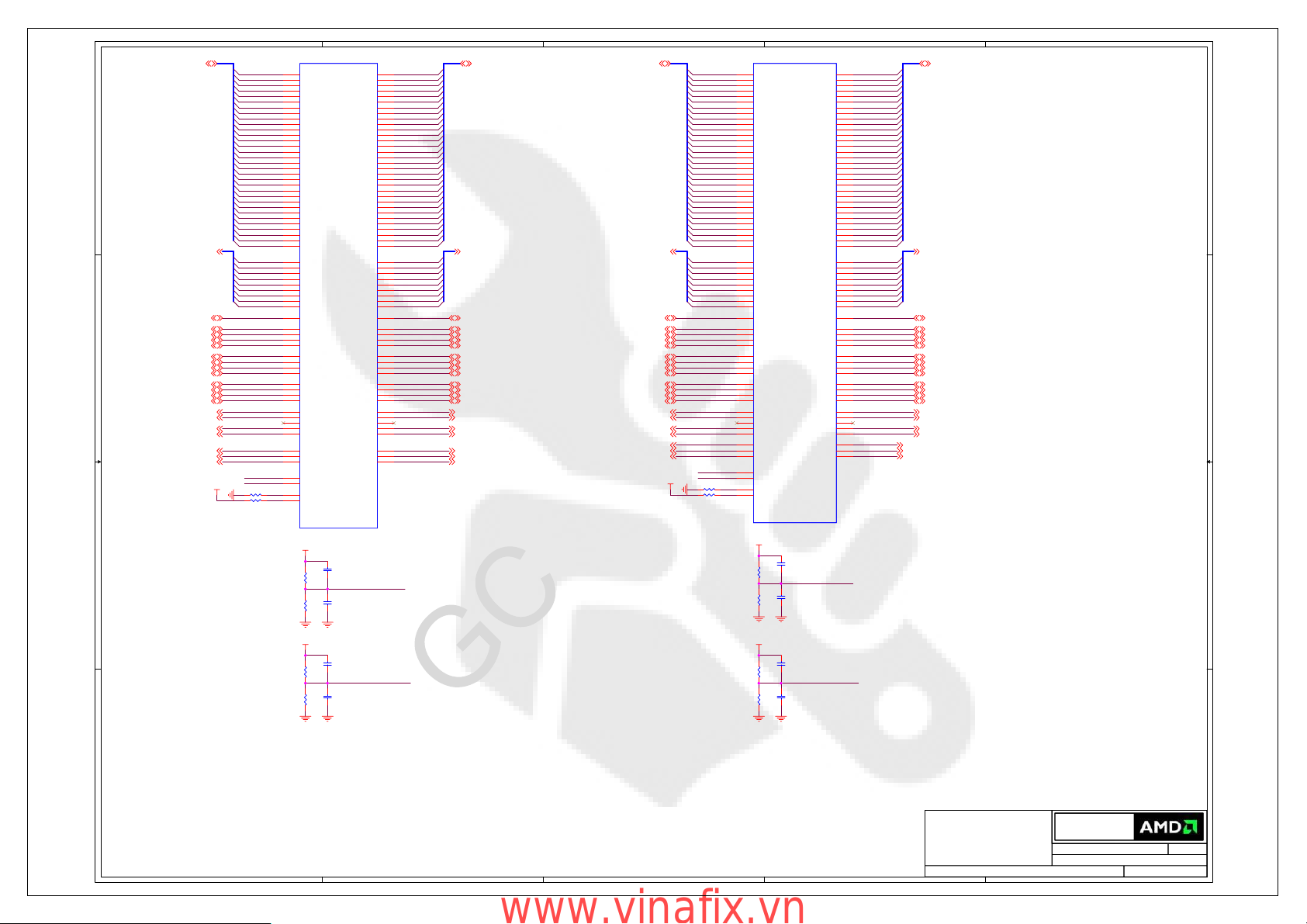
5
U1E
W12
W13
AA14
W11
AA10
W14
AA11
AA16
AA15
E4
H4
G2
F6
J5
K6
K4
L1
V10
V11
U11
U12
L11
M11
M10
M9
M6
M4
N3
N1
P6
R3
R1
R5
Y6
W3
Y4
W5
V4
U3
U5
U1
V9
V14
V16
U13
V15
AA9
L3
L5
T4
T6
H6
R10
N5
W1
J3
R9
P4
V6
R14
R13
P11
P13
P12
U16
V17
U1E
DQC0_0
DQC0_1
DQC0_2
DQC0_3
DQC0_4
DQC0_5
DQC0_6
DQC0_7
DQC0_8
DQC0_9
DQC0_10
DQC0_11
DQC0_12
DQC0_13
DQC0_14
DQC0_15
DQC0_16
DQC0_17
DQC0_18
DQC0_19
DQC0_20
DQC0_21
DQC0_22
DQC0_23
DQC0_24
DQC0_25
DQC0_26
DQC0_27
DQC0_28
DQC0_29
DQC0_30
DQC0_31
MAC0_0
MAC0_1
MAC0_2
MAC0_3
MAC0_4
MAC0_5
MAC0_6
MAC0_7
MAC0_8
ADBIC0
WCKC0_0
WCKC0B_0
WCKC0_1
WCKC0B_1
EDCC0_0
EDCC0_1
EDCC0_2
EDCC0_3
DDBIC0_0
DDBIC0_1
DDBIC0_2
DDBIC0_3
WEC0B
CSC0B_0
CSC0B_1
CASC0B
RASC0B
CKEC0
CLKC0
CLKC0B
MVREFCS
MVREFCD
MEM_CALRPC
MEM_CALRNC
RV770 GL A11
RV770 GL A11
+MVDDQ
R139
R139
40.2R
40.2R
1%
R141
R141
100R
100R
1%
+MVDDQ
R143
R143
40.2R
40.2R
1%
R145
R145
100R
100R
1%
WCKC1_0
WCKC1B_0
WCKC1_1
WCKC1B_1
DDBIC1_0
DDBIC1_1
DDBIC1_2
DDBIC1_3
C311
C311
NC_1uF_6.3V
NC_1uF_6.3V
C315
C315
1uF_6.3V
1uF_6.3V
C319
C319
NC_1uF_6.3V
NC_1uF_6.3V
C323
C323
1uF_6.3V
1uF_6.3V
DQC1_0
DQC1_1
DQC1_2
DQC1_3
DQC1_4
DQC1_5
DQC1_6
DQC1_7
DQC1_8
DQC1_9
DQC1_10
DQC1_11
DQC1_12
DQC1_13
DQC1_14
DQC1_15
DQC1_16
DQC1_17
DQC1_18
DQC1_19
DQC1_20
DQC1_21
DQC1_22
DQC1_23
DQC1_24
DQC1_25
DQC1_26
DQC1_27
DQC1_28
DQC1_29
DQC1_30
DQC1_31
MAC1_0
MAC1_1
MAC1_2
MAC1_3
MAC1_4
MAC1_5
MAC1_6
MAC1_7
MAC1_8
ADBIC1
EDCC1_0
EDCC1_1
EDCC1_2
EDCC1_3
WEC1B
CSC1B_0
CSC1B_1
CASC1B
RASC1B
CKEC1
CLKC1
CLKC1B
MVREFD_C
MVREFS_C
AR16
AN14
AR14
AR15
AM15
AM14
AK13
AK14
AJ15
AH12
AH13
AF10
AF9
AF16
AE13
AE12
AJ3
AJ1
AH4
AH6
AG1
AF4
AE5
AF6
AA5
AB4
AA3
AA1
AC5
AD6
AD4
AC3
AD9
AD11
AE11
AD14
AH11
AE14
AB13
AB14
AB11
AB12
AJ10
AJ11
AE3
AE1
AN13
AF11
AG5
AB6
AN12
AF12
AG3
AC1
AJ16
AF14
AF15
AD15
AD10
AD16
AJ14
AH14
MVREFD/S =0.7*
VDDR1
(GDDR3/4/5)
DQC0_[31..0](9)
D D
MAC0_[8..0](9)
ADBIC0(9)
WCKC0_0(9)
WCKC0b_0(9)
WCKC0_1(9)
WCKC0b_1(9)
C C
B B
EDCC0_0(9)
EDCC0_1(9)
(9)
EDCC0_2
EDCC0_3(9)
DDBIC0_0(9)
DDBIC0_1(9)
DDBIC0_2(9)
DDBIC0_3(9)
DQC0_0
DQC0_1
DQC0_2
DQC0_3
DQC0_4
DQC0_5
DQC0_6
DQC0_7
DQC0_8
DQC0_9
DQC0_10
DQC0_11
DQC0_12
DQC0_13
DQC0_14
DQC0_15
DQC0_16
DQC0_17
DQC0_18
DQC0_19
DQC0_20
DQC0_21
DQC0_22
DQC0_23
DQC0_24
DQC0_25
DQC0_26
DQC0_27
DQC0_28
DQC0_29
DQC0_30
DQC0_31
MAC0_0
MAC0_1
MAC0_2
MAC0_3
MAC0_4
MAC0_5
MAC0_6
MAC0_7
MAC0_8
WEC0b(9)
CSC0b_0(9)
CASC0b(9)
RASC0b(9)
CKEC0(9)
CLKC0(9)
CLKC0b(9)
+MVDDQ
MVREFS_C
MVREFD_C
R135 243RR135 243R
R137 243RR137 243R
DQC1_0
DQC1_1
DQC1_2
DQC1_3
DQC1_4
DQC1_5
DQC1_6
DQC1_7
DQC1_8
DQC1_9
DQC1_10
DQC1_11
DQC1_12
DQC1_13
DQC1_14
DQC1_15
DQC1_16
DQC1_17
DQC1_18
DQC1_19
DQC1_20
DQC1_21
DQC1_22
DQC1_23
DQC1_24
DQC1_25
DQC1_26
DQC1_27
DQC1_28
DQC1_29
DQC1_30
DQC1_31
MAC1_0
MAC1_1
MAC1_2
MAC1_3
MAC1_4
MAC1_5
MAC1_6
MAC1_7
MAC1_8
4
DQC1_[31..0] (9)
MAC1_[8..0] (9)
ADBIC1 (9)
WCKC1_0 (9)
WCKC1b_0 (9)
WCKC1_1 (9)
WCKC1b_1 (9)
EDCC1_0 (9)
EDCC1_1 (9)
EDCC1_2 (9)
EDCC1_3 (9)
DDBIC1_0 ( 9)
DDBIC1_1 ( 9)
DDBIC1_2 ( 9)
DDBIC1_3 ( 9)
WEC1b (9)
CSC1b_0 (9)
CASC1b (9)
RASC1b (9)
CKEC1 (9)
CLKC1 (9)
CLKC1b (9)
機
3
U1F
DQD0_[31..0](9)
MAD0_[8..0](9)
ADBID0(9)
WCKD0_0(9)
WCKD0b_0(9)
WCKD0_1(9)
WCKD0b_1(9)
EDCD0_0(9)
EDCD0_1(9)
EDCD0_2(9)
EDCD0_3(9)
DDBID0_0(9)
DDBID0_1(9)
DDBID0_2(9)
DDBID0_3(9)
DQD0_0
DQD0_1
DQD0_2
DQD0_3
DQD0_4
DQD0_5
DQD0_6
DQD0_7
DQD0_8
DQD0_9
DQD0_10
DQD0_11
DQD0_12
DQD0_13
DQD0_14
DQD0_15
DQD0_16
DQD0_17
DQD0_18
DQD0_19
DQD0_20
DQD0_21
DQD0_22
DQD0_23
DQD0_24
DQD0_25
DQD0_26
DQD0_27
DQD0_28
DQD0_29
DQD0_30
DQD0_31
MAD0_0
MAD0_1
MAD0_2
MAD0_3
MAD0_4
MAD0_5
MAD0_6
MAD0_7
MAD0_8
WED0b(9)
CSD0b_0(9)
CASD0b(9)
RASD0b(9)
CKED0(9)
CLKD0(9)
CLKD0b(9)
MVREFS_D
MVREFD_D
+MVDDQ
密
R134 243RR134 243R
R136 243RR136 243R
U1F
AJ5
DQD0_0
AK6
DQD0_1
AK4
DQD0_2
AL1
DQD0_3
AM6
DQD0_4
AM4
DQD0_5
AN5
DQD0_6
AN3
DQD0_7
AR11
DQD0_8
AK12
DQD0_9
AR10
DQD0_10
AR9
DQD0_11
AN11
DQD0_12
AK11
DQD0_13
AJ9
DQD0_14
AM11
DQD0_15
AR3
DQD0_16
AR1
DQD0_17
AP6
DQD0_18
AR5
DQD0_19
AU1
DQD0_20
AU3
DQD0_21
AU5
DQD0_22
AV2
DQD0_23
BB6
DQD0_24
BA5
DQD0_25
BC1
DQD0_26
BB4
DQD0_27
AY6
DQD0_28
AW5
DQD0_29
AW3
DQD0_30
AY4
DQD0_31
BB9
MAD0_0
AY10
MAD0_1
AU11
MAD0_2
AY9
MAD0_3
AU9
MAD0_4
AU10
MAD0_5
AW12
MAD0_6
AY12
MAD0_7
BB10
MAD0_8
BB11
ADBID0
AP2
WCKD0_0
AP4
WCKD0B_0
AV4
WCKD0_1
AV6
WCKD0B_1
AL3
EDCD0_0
AM9
EDCD0_1
AT4
EDCD0_2
BA3
EDCD0_3
AL5
DDBID0_0
AM10
DDBID0_1
AT6
DDBID0_2
BA1
DDBID0_3
文件
AT13
WED0B
AU14
CSD0B_0
AU15
CSD0B_1
AW13
CASD0B
AW11
RASD0B
AU16
CKED0
AT12
CLKD0
AT11
CLKD0B
AM17
MVREFDS
AN17
MVREFDD
AM16
MEM_CALRPD
AT14
MEM_CALRND
RV770 GL A11
RV770 GL A11
+MVDDQ
R138
R138
40.2R
40.2R
1%
R140
R140
100R
100R
1%
+MVDDQ
R142
R142
40.2R
40.2R
1%
R144
R144
100R
100R
1%
C309
C309
NC_1uF_6.3V
NC_1uF_6.3V
C313
C313
1uF_6.3V
1uF_6.3V
C317
C317
NC_1uF_6.3V
NC_1uF_6.3V
C321
C321
1uF_6.3V
1uF_6.3V
DQD1_0
DQD1_1
DQD1_2
DQD1_3
DQD1_4
DQD1_5
DQD1_6
DQD1_7
DQD1_8
DQD1_9
DQD1_10
DQD1_11
DQD1_12
DQD1_13
DQD1_14
DQD1_15
DQD1_16
DQD1_17
DQD1_18
DQD1_19
DQD1_20
DQD1_21
DQD1_22
DQD1_23
DQD1_24
DQD1_25
DQD1_26
DQD1_27
DQD1_28
DQD1_29
DQD1_30
DQD1_31
MAD1_0
MAD1_1
MAD1_2
MAD1_3
MAD1_4
MAD1_5
MAD1_6
MAD1_7
MAD1_8
ADBID1
WCKD1_0
WCKD1B_0
WCKD1_1
WCKD1B_1
EDCD1_0
EDCD1_1
EDCD1_2
EDCD1_3
DDBID1_0
DDBID1_1
DDBID1_2
DDBID1_3
WED1B
CSD1B_0
CSD1B_1
CASD1B
RASD1B
CKED1
CLKD1
CLKD1B
MVREFD_D
MVREFD/S =0.7*
VDDR1
(GDDR3/4/5)
MVREFS_D
BC18
BB18
BA18
AY18
BE17
BA15
BB15
BD14
BH12
BK12
BN11
BL11
BH14
BK14
BM14
BN13
BJ11
BK10
BM7
BL9
BH10
BH8
BH6
BL3
BC5
BD4
BC3
BF1
BD6
BF6
BF4
BG2
BD11
BE12
AY14
BD12
BC15
BC14
BC9
BD10
BC11
BE10
BL15
BJ15
BK5
BJ4
BD17
BJ13
BJ9
BE3
BC17
BL13
BK8
BE5
AV17
AW15
AY15
BD9
BE14
BB12
AY17
AW17
2
DQD1_0
DQD1_1
DQD1_2
DQD1_3
DQD1_4
DQD1_5
DQD1_6
DQD1_7
DQD1_8
DQD1_9
DQD1_10
DQD1_11
DQD1_12
DQD1_13
DQD1_14
DQD1_15
DQD1_16
DQD1_17
DQD1_18
DQD1_19
DQD1_20
DQD1_21
DQD1_22
DQD1_23
DQD1_24
DQD1_25
DQD1_26
DQD1_27
DQD1_28
DQD1_29
DQD1_30
DQD1_31
MAD1_0
MAD1_1
MAD1_2
MAD1_3
MAD1_4
MAD1_5
MAD1_6
MAD1_7
MAD1_8
WED1b (9)
CKED1 (9)
CLKD1 (9)
CLKD1b (9)
DQD1_[31..0] (9)
MAD1_[8..0] (9)
ADBID1 (9)
WCKD1_0 (9)
WCKD1b_0 (9)
WCKD1_1 (9)
WCKD1b_1 (9)
EDCD1_0 (9)
EDCD1_1 (9)
EDCD1_2 (9)
EDCD1_3 (9)
DDBID1_0 ( 9)
DDBID1_1 ( 9)
DDBID1_2 ( 9)
DDBID1_3 ( 9)
CSD1b_0 (9)
CASD1b (9)
RASD1b (9)
1
A A
5
4
Printed with FinePrint - purchase at www.fineprint.com
3
www.vinafix.vn
CONFIDENTIAL & PROPRIETARY TO ADVANCED MICRO DEVICES INC.
CONFIDENTIAL & PROPRIETARY TO ADVANCED MICRO DEVICES INC.
CONFIDENTIAL & PROPRIETARY TO ADVANCED MICRO DEVICES INC.
?2007 Advanced Micro D evices
?2007 Advanced Micro D evices
?2007 Advanced Micro D evices
This AMD Board schemat ic and desi gn is the exclu sive pr opert y o f AMD,
This AMD Board schemat ic and desi gn is the exclu sive pr opert y o f AMD,
This AMD Board schemat ic and desi gn is the exclu sive pr opert y o f AMD,
and is provided only to entiti es under a non -disclosure agreement
and is provided only to entiti es under a non -disclosure agreement
and is provided only to entiti es under a non -disclosure agreement
with AMD for evalu ation purposes. F urther distribut ion or di sclosure
with AMD for evalu ation purposes. F urther distribut ion or di sclosure
with AMD for evalu ation purposes. F urther distribut ion or di sclosure
is strictly prohibited. Use of th is sch ematic and de sign fo r any pu rpose
is strictly prohibited. Use of th is sch ematic and de sign fo r any pu rpose
is strictly prohibited. Use of th is sch ematic and de sign fo r any pu rpose
other than evaluation re quires a Board T echnology License Agre ement
other than evaluation re quires a Board T echnology License Agre ement
other than evaluation re quires a Board T echnology License Agre ement
with AMD. AMD makes no r epre sentat ions or war ranties of an y kind
with AMD. AMD makes no r epre sentat ions or war ranties of an y kind
with AMD. AMD makes no r epre sentat ions or war ranties of an y kind
regarding this schemat ic and design , in cluding, n ot limit ed to,
regarding this schemat ic and design , in cluding, n ot limit ed to,
regarding this schemat ic and design , in cluding, n ot limit ed to,
any implied warranty of mer chanti bility or fitness for a par ticular
any implied warranty of mer chanti bility or fitness for a par ticular
any implied warranty of mer chanti bility or fitness for a par ticular
purpose, and disclaims respons ibility forany co nsequences resul ting
purpose, and disclaims respons ibility forany co nsequences resul ting
purpose, and disclaims respons ibility forany co nsequences resul ting
from use of the information include d herein .
from use of the information include d herein .
from use of the information include d herein .
Title
Title
2
Title
RH RV770 GDDR5 DVI-I VO DVI-I FH
RH RV770 GDDR5 DVI-I VO DVI-I FH
RH RV770 GDDR5 DVI-I VO DVI-I FH
Advanced Micro Devices Inc.
Advanced Micro Devices Inc.
Advanced Micro Devices Inc.
1 Commerce Valley Drive East
1 Commerce Valley Drive East
1 Commerce Valley Drive East
Markham, Ontario
Markham, Ontario
Markham, Ontario
Thursday, October 09, 2008
Thursday, October 09, 2008
Thursday, October 09, 2008
Sheet
Sheet
Sheet
622
622
622
of
of
of
1
Doc No.
Doc No.
Doc No.
RevDate:
RevDate:
RevDate:
1
1
1
105-B507xx-10
105-B507xx-10
105-B507xx-10
Page 7
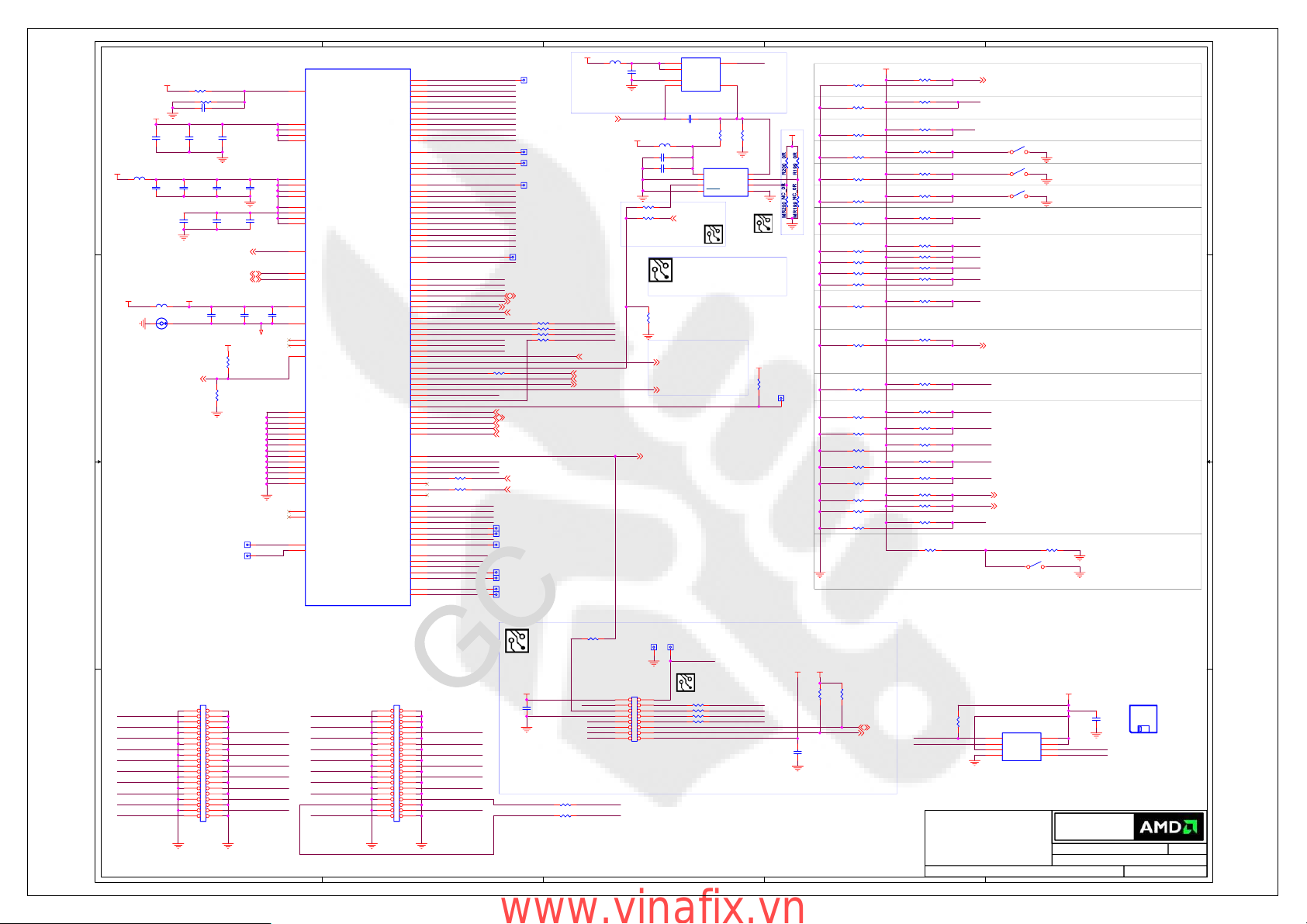
5
U1K
+1.8V
R147 221RR147 221R
R151 110RR151 110R
C328 100nF_6.3VC328 100nF_6.3V
+3.3V
C332
C332
C333
C333
100nF_6.3V
100nF_6.3V
100nF_6.3V
C325
C325
10uF_X6S
10uF_X6S
+TSVDD
NS8NS_VIA NS8NS_VIA
12
JTAG_MODE(1)
100nF_6.3V
C335
C335
1uF_6.3V
1uF_6.3V
C329
C329
1uF_6.3V
1uF_6.3V
1uF_6.3V
1uF_6.3V
C365
C365
D D
+1.8V
B113
B113
BLM15BD121SN1
BLM15BD121SN1
+1.8V
BLM15BD121SN1
BLM15BD121SN1
B119
B119
C C
B B
TS_FDO(19)
GPU_DPLUS(19)
GPU_DMINUS(19)
100nF_6.3V
100nF_6.3V
DNI
C334
C334
100nF_6.3V
100nF_6.3V
C326
C326
100nF_6.3V
100nF_6.3V
C330
C330
100nF_6.3V
100nF_6.3V
C366
C366
+3.3V
MR170
MR170
NC_10K
NC_10K
R1701KR170
1K
TP4008
TP4009
TP4009
VREFG
C327
C327
1uF_6.3V
1uF_6.3V
C331
C331
1uF_6.3V
1uF_6.3V
C367
C367
10nF
10nF
GND_TSVSS
JTAG_MODE
35mil
35mil
35mil
35mil
BG21
AU29
AU30
AU32
AU33
BB24
BE24
BC24
BD24
BE25
BD25
BB25
BC25
AV36
AV30
AW30
AU24
AU25
BA30
BB30
AU39
BG19
BA22
AV28
BA29
BA35
AW36
BA26
AY30
BM22
BN19
AU22
BG43
AU28
AU26
AR19
AP19
BA19
AY19
U1K
VREFG
VDDR3#1
VDDR3#2
VDDR3#3
VDDR3#4
VDDR5#1
VDDR5#2
VDDR5#3
VDDR5#4
VDDR4#1
VDDR4#2
VDDR4#3
VDDR4#4
TS_FDO
DPLUS
DMINUS
TSVDD
TSVSS
RSVD#1
RSVD#2
JMODE
VSSD#1
VSSD#2
VSSD#3
VSSD#4
VSSD#5
VSSD#6
VSSD#7
VSSD#8
VSSD#9
VSSD#10
VSSD#11
VSSD#12
VSSD#13
VSSD#14
NC_GPIO_31
NC_GPIO_32
TEST_YCLK
TEST_MCLK
RV770 GL A11
RV770 GL A11
DVPDATA_0
DVPDATA_1
DVPDATA_2
DVPDATA_3
DVPDATA_4
DVPDATA_5
DVPDATA_6
DVPDATA_7
DVPDATA_8
DVPDATA_9
DVPDATA_10
DVPDATA_11
DVPCNTL_0
DVPCNTL_1
DVPCNTL_2
DVPDATA_12
DVPDATA_13
DVPDATA_14
DVPDATA_15
DVPDATA_16
DVPDATA_17
DVPDATA_18
DVPDATA_19
DVPDATA_20
DVPDATA_21
DVPDATA_22
DVPDATA_23
DVPCNTL_MVP_0
DVPCNTL_MVP_1
GPIO_3_SMBDAT
GPIO_4_SMBCLK
GPIO_6_TACH
GPIO_8_ROMSO
GPIO_9_ROMSI
GPIO_10_ROMSCK
GPIO_11
GPIO_12
GPIO_13
GPIO_14_HPD2
GPIO_15_PWRCNTL_ 0
GPIO_16_SSIN
GPIO_17_THERMAL_INT
GPIO_18_HPD3
GPIO_19_CTF
GPIO_20_PWRCNTL_ 1
GPIO_21
GPIO_22_ROMCSB
GPIO_23_CLKREQB
GPIO_24_TRSTB
GPIO_25_TDI
GPIO_26_TCK
GPIO_27_TMS
GPIO_28_TDO
GENERICA
GENERICB
GENERICC
GENERICD
GENERICE
GENERICF
GENERICG
GENERICH
CrossFire Card-Edge
Lower Cable Card Edge
1
DVOCLK
DVPCNTL_2
DVPDATA_1
DVPDATA_3
DVPDATA_5
DVPDATA_7
A A
DVPDATA_9
DVPDATA_11
DVPCNTL_1
GENERICD
3
5
7
9
11
13
15
17
19
21
23
25
27
29 30
31
33
35
37
39
J1J1
2
4
6
8
DVPDATA_0
10
12
DVPDATA_2
14
16
DVPDATA_4
18
20
DVPDATA_6
22
24
DVPDATA_8
26
28
DVPDATA_10
32
DVPCNTL_0
34
36
GPIO_2
38
40
Bundle B
5
Upper Cable Card Edge
DVP_MVP_CNTL_1
DVP_MVP_CNTL_0
DVPDATA_13
DVPDATA_15
DVPDATA_17
DVPDATA_19
DVPDATA_21
DVPDATA_23
GENERICB_R
GENERICC
11
13
15
17
19
21
23
25
27
29 30
31
33
35
37
39
Bundle A (closer to the bracket)
DVPCLK
GPIO_0
GPIO_1
GPIO_2
GPIO_5
GPIO_7
VIP_0
VIP_1
VIP_2
VIP_3
VIP_4
VIP_5
VIP_6
VIP_7
VPCLK0
DVALID
PSYNC
VHAD_0
VHAD_1
VPHCTL
VIPCLK
1
3
5
7
9
J2J2
BH20
BK20
BM20
BJ21
BL21
BN21
BH22
BK22
BG23
BJ23
BN23
BL23
BK18
BM18
BJ19
BL19
AW25
AY24
AV25
AY25
AY26
AW26
BA28
AV26
AY28
AW28
AY29
AW29
AW24
AV24
BA24
AV29
BH24
BD22
BA25
BE22
AY22
BC22
BB22
BA21
BB21
AW22
BE21
BD21
BD19
BB19
BC19
BE19
AY21
BH18
BN17
BG17
BC21
AW21
BL17
BM16
BH16
BK16
BJ17
BC35
BE32
BC33
BA33
BC30
BD35
BB29
BD32
AV35
AW35
AY35
AV33
AW33
AY33
AV32
AW32
AY32
BB33
BE35
AU36
AU35
BB35
BA32
2
4
6
8
10
12
14
16
18
20
22
24
26
28
32
34
36
38
40
4
DVPDATA_0
DVPDATA_1
DVPDATA_2
DVPDATA_3
DVPDATA_4
DVPDATA_5
DVPDATA_6
DVPDATA_7
DVPDATA_8
DVPDATA_9
DVPDATA_10
DVPDATA_11
DVOCLK
DVPCNTL_0
DVPCNTL_1
DVPCNTL_2
DVPDATA_12
DVPDATA_13
DVPDATA_14
DVPDATA_15
DVPDATA_16
DVPDATA_17
DVPDATA_18
DVPDATA_19
DVPDATA_20
DVPDATA_21
DVPDATA_22
DVPDATA_23
DVP_MVP_CNTL_0
DVP_MVP_CNTL_1
GPIO_0
GPIO_1
GPIO_2
GPIO_3
GPIO_4
GPIO_5
GPIO_6
GPIO_7
GPIO_8
GPIO_9
GPIO_10
GPIO_11
GPIO_12
GPIO_13
HPD2
G1_GPIO_15_PWRCNTL_0
GPIO_16
GPIO_17_INT
GPIO_19_CTF
G1_GPIO_20_PWRCNTL_1
GPIO_21
GPIO_22_ROMCSb
PCIE_CLK_REQb
JTAG_TRSTB
JTAG_TDI
JTAG_TCK
JTAG_TMS
JTAG_TDO
GENERICA
GENERICB
GENERICC
GENERICD
R198 0RR198 0R
R204 0RR204 0R
VIP_0
VIP_1
VIP_2
VIP_3
VIP_6
DVALIDDVALID
PSYNCPSYNC
VHAD_0
DVPDATA_12
DVPDATA_14
DVPDATA_16
DVPDATA_18
DVPDATA_20
DVPDATA_22
DVALID_R
GPIO_1
4
TP400535mil TP400535mil
CrossFire
TP400335mil TP400335mil
TP400435mil TP400435mil
TP400635mil TP400635mil
+1.8V
NC_BLM15BD121SN1
NC_BLM15BD121SN1
B125
B125
NC_100nF_6.3V
NC_100nF_6.3V
1.8V to 3.3V translator option
SSCLKIN(3)
C398
C398
+3.3V
BLM15BD121SN1
BLM15BD121SN1
B124
B124
C397 1uF_6.3VC397 1uF_6.3V
C395 100nF_6.3VC395 100nF_6.3V
R197 0RR197 0R
MR197
MR197
3
NC_0R
NC_0R
Share pad
TP4007
TP4007
DVP_MVP_CNTL_0 : DE for bits D[ 12..23]
35mil
35mil
DVP_MVP_CNTL_1 : CLK for bits D[12..23]
CrossFire
FLOW_CONTROL_1 - Lower Cable
GPIO_3 (1)
FLOW_CONTROL_2 - U pper C a ble
GPIO_4 (1)
SWAP_LOCK_1 - Lower Cable
GPIO_5 (17)
SWAP_LOCK_2 - Upper C able
TACH (19)
R162 NC_0RR162 NC_0R
JTAG_TRSTB (1)
JTAG_TDI (1)
JTAG_TCK (1)
JTAG_TMS (1)
JTAG_TDO (1)
EXT_12V_DET (17)
EXT_12V_DET_B (17)
TP401135mil TP401135mil
TP401235mil TP401235milTP4008
TP401335mil TP401335mil
TP401735mil TP401735mil
TP401635mil TP401635mil
TP401035mil TP401035mil
TP401435mil TP401435mil
TP401535mil TP401535mil
Place it at top edge of the
board on the bottom side.
In production, this block
will not be populated.
Mating connector: 6010028300G
(HEADER 2X8 1.27MM PITCH, SMD)
When attaching the daughter card (B176) align it by mounting hole.
+3.3V
TC1
TC1
NC_100nF_6.3V
NC_100nF_6.3V
R181 NC_0RR181 NC_0 R
R182 NC_0RR182 NC_0 R
GENERICB: Generic I2C_SDA
DVALID: Generic I2C_SCL
RP1A33R RP1A33R
GPIO_8_R
81
GPIO_9_R
RP1B33R RP1B33R
72
GPIO_10_R
RP1C33R RP1C33R
63
ROMCSb_R
RP1D33R RP1D33R
54
HPD2 (16)
ThermINT (17,19)
REG_THERM_INT# (17)
GPIO_19_CTF (17)
機
TR2 NC_0RTR2 NC_0R
DNI
JTAG_MODE
JTAG_TCK
JTAG_TMS
JTAG_TDI
JTAG_TDO
DNI
DVALID
DNI
GENERICB
BUO
TJ1
TJ1
2
1
4
3
6
5
8
7
10
9
12
11
14
13
16
15
NC_2X8SOCKET
NC_2X8SOCKET
R203
R203
NC_150R
NC_150R
Place close to U1
GPIOs for VDDC Setting
GENERICA (18)
TP30
TP30
35mil
35mil
GPIO_8_T
ROMCSb_T
GPIO_9_T
GPIO_10_T
SDA
SCL
3
U14
U14
1
VCCA
5
DIR
2
GND
A3B
NC_DIGPOT_10K
NC_DIGPOT_10K
C396
C396
10nF_25V
10nF_25V
SS_VCC
8
7
6
5
EXT_12V_DET (17)
Place SW1 & SW2 on the bottom side
(easily accessible).
Clearly Mark A & B contacts on the
silkscreen.
G1_GPIO_15_PWRCNTL_0 (11)
G1_GPIO_20_PWRCNTL_1 (11)
VCCB
VCC
CRSEL
SSO
SSEN
6
4
R201
R201
100K
100K
CLKIN
SMSEL1
SMSEL2
DS1081LE
DS1081LE
SS_VCC
R202
R202
100K
100K
U13
U13
1
2
3
4
GND
+3.3V
文件
密
TP31
TP31
35mil
35mil
For wire soldering
EXT_ADJ_1.8V
Place TRP1 & TR2 in a way
to minimize the stub when
they are not populated.
NC_33R
NC_33R
TRP1D
TRP1D
GPIO_8_R
54
NC_33R
NC_33R
TRP1C
TRP1C
ROMCSb_R
63
GPIO_9_R
TRP1BNC_33R TRP1BNC_33R
72
GPIO_10_R
TRP1ANC_33R TRP1ANC_33R
81
2
+3.3V
DNI
MR146 NC_10KMR146 NC_10K
DNI
MR150 NC_10KMR150 NC_10K
+3.3V
Share padPlace close to U13
TR1
TR1
10K
10K
35mil
35mil
TP29
TP29
MR148 10KMR148 10K
DNI
MR149 NC_10KMR149 NC_10K
DNI
MR152 NC_10KMR152 NC_10K
DNI
MR153 10KMR153 10K
MR155 NC_10KMR155 NC_10K
MR156 10KMR156 10K
DNI
MR157 NC_10KMR157 NC_10K
MR158 10KMR158 10K
MR159 NC_10KMR159 NC_10K
MR160 NC_10KMR160 NC_10K
MR161 10KMR161 10K
MR163 10KMR163 10K
MR164 NC_10KMR164 NC_10K
DNI
MR165 NC_10KMR165 NC_10K
MR166 NC_10KMR166 NC_10K
MR167 NC_10KMR167 NC_10K
MR168 NC_10KMR168 NC_10K
MR169 NC_10KMR169 NC_10K
MR173 NC_10KMR173 NC_10K
MR175 NC_10KMR175 NC_10K
Pull-Down Resistors are for BU until built-in pull-downs are verified.
+3.3V+5V
TR4
TR4
TR3
TR3
NC_4.7K
NC_4.7K
NC_4.7K
NC_4.7K
BUOBUO
SDA (3)
SCL (3)
TC2
TC2
NC_100nF_6.3V
NC_100nF_6.3V
2
PIN BASED STRAPS
R146 10KR146 10K
R150 10KR150 10K
DNI
R148 NC_10KR1 48 NC_10K
R149 10KR149 10K
R152 10KR152 10K
R153 NC_10KR1 53 NC_10K
DNI
R155 NC_10KR155 NC_10K
DNI
R156
R156
R157 10KR157 10K
DNI
R158 NC_10K
R158 NC_10K
DNI
R159 10KR159 10K
R160 10KR160 10K
R161 NC_10KR1 61 NC_10K
DNI
R163 NC_10KR1 63 NC_10K
DNI
R164 NC_10KR164 NC_10K
DNI
R165
R165
DNI
R166 NC_10KR166 NC_10K
DNI
R167 NC_10KR167 NC_10K
DNI
R168 NC_10KR168 NC_10K
DNI
R169 NC_10KR169 NC_10K
DNI
R173 NC_10KR173 NC_10K
DNI
R175 NC_10KR175 NC_10K
NTSC
VSYNC
VHAD_0
PSYNC
GPIO_0
GPIO_1
GPIO_2
VIP_1
NC_10K
NC_10K
GPIO_9_R
GPIO_13
GPIO_12
GPIO_11
GPIO_8
HSYNC1
DVALID
VIP_6
NC_10K
NC_10K
VIP_3
VIP_2
VIP_0
GPIO_21
VSYNC2
HSYNC2
GENERICC
GPIO_7
R176 10KR176 10K
R180
R180
10K
10K
ROMCSb_R
GPIO_8_R
PN 2280007900G for 1Mbit (PM25LV010A-100SCE)
CONFIDENTIAL & PROPRIETARY TO ADVANCED MICRO DEVICES INC.
CONFIDENTIAL & PROPRIETARY TO ADVANCED MICRO DEVICES INC.
CONFIDENTIAL & PROPRIETARY TO ADVANCED MICRO DEVICES INC.
?2007 Advanced Micro D evices
?2007 Advanced Micro D evices
?2007 Advanced Micro D evices
This AMD Board schemat ic and desi gn is the exclu sive pr opert y o f AMD,
This AMD Board schemat ic and desi gn is the exclu sive pr opert y o f AMD,
This AMD Board schemat ic and desi gn is the exclu sive pr opert y o f AMD,
and is provided only to entiti es under a non -disclosure agreement
and is provided only to entiti es under a non -disclosure agreement
and is provided only to entiti es under a non -disclosure agreement
with AMD for evalu ation purposes. F urther distribut ion or di sclosure
with AMD for evalu ation purposes. F urther distribut ion or di sclosure
with AMD for evalu ation purposes. F urther distribut ion or di sclosure
is strictly prohibited. Use of th is sch ematic and de sign fo r any pu rpose
is strictly prohibited. Use of th is sch ematic and de sign fo r any pu rpose
is strictly prohibited. Use of th is sch ematic and de sign fo r any pu rpose
other than evaluation re quires a Board T echnology License Agre ement
other than evaluation re quires a Board T echnology License Agre ement
other than evaluation re quires a Board T echnology License Agre ement
with AMD. AMD makes no r epre sentat ions or war ranties of an y kind
with AMD. AMD makes no r epre sentat ions or war ranties of an y kind
with AMD. AMD makes no r epre sentat ions or war ranties of an y kind
regarding this schemat ic and design , in cluding, n ot limit ed to,
regarding this schemat ic and design , in cluding, n ot limit ed to,
regarding this schemat ic and design , in cluding, n ot limit ed to,
any implied warranty of mer chanti bility or fitness for a par ticular
any implied warranty of mer chanti bility or fitness for a par ticular
any implied warranty of mer chanti bility or fitness for a par ticular
purpose, and disclaims respons ibility forany co nsequences resul ting
purpose, and disclaims respons ibility forany co nsequences resul ting
purpose, and disclaims respons ibility forany co nsequences resul ting
from use of the information include d herein .
from use of the information include d herein .
from use of the information include d herein .
Title
Title
Title
RH RV770 GDDR5 DVI-I VO DVI-I FH
RH RV770 GDDR5 DVI-I VO DVI-I FH
RH RV770 GDDR5 DVI-I VO DVI-I FH
VSYNC1 (3,15)
SW1A
SW1A
NC_DIP_SWX2
NC_DIP_SWX2
SW1B
SW1B
NC_DIP_SWX2
NC_DIP_SWX2
SW2A
SW2A
NC_DIP_SWX2
NC_DIP_SWX2
HSYNC1 (3,15)
VSYNC2 (3,16)
HSYNC2 (3,16)
U2
U2
1
CE#
2
SO
3
WP#
GND4SI
PM25LV010-25SCE
PM25LV010-25SCE
1
VIP_DEVICE_STRAP_EN
0: Slave VIP host port devices present (use if Theater is populated)
1: No slave VIP host port devices reporting presence during reset (use for
configurations without video-in)
If VIP_DEVICE_STRAP_EN is set to ?? then this pin is
used to sense whether a VIP slave de vic e is co nne cted to
the VIP Host interface. If VIP_DEVICE_STRAP_EN is set
to ?? then this pin is not used as a strap at all
VGA DISABLE : 1 for disable (s et to 0 for nor ma l operatio n)
GPIO(0) - TX_PWRS_ENB (Tra nsmi tter Pow er Sav ings Enable)
41
0: 50% Tx output swing for mobi le mo de
1: full Tx output swing (Default se tti ng for De skt op)
GPIO(1) - TX_DEEMPH_EN (Transmitter D e-emphasis E na ble)
32
0: Tx de-emphasis disabled for mobile mode
1: Tx de-emphasis enabled (Default setti ng for Des ktop)
GPIO(2) - BIF_GEN2_EN (5.0 GT/s Enable)
41
1 : Allows either PCIe 2.5 GT/s or 5.0 GT /s opera tion
0 : Debug use only (disables PCIe 5.0 GT/s negotiation)
MSI_DIS (Default: 0)
Disable Message Signaled Interrupt is both a RO M strap
and a pin strap. The pin strap is only applicable i f a B IOS
ROM is not present.
GPIO(9,13, 12,11) - CONFIG[3..0]
CONFIG[3]
0100 - 512Kbit M25P05A (S T)
0101 - 1Mbit M25P10A (ST)
CONFIG[2]
0101 - 2Mbit M25P20 (ST)
0101 - 4Mbit M25P40 (ST)
CONFIG[1]
0101 - 8Mbit M25P80 (ST)
0100 - 512Kbit Pm25LV512 (Chingis)
CONFIG[0]
0101 - 1Mbit Pm25LV010 (Chingis)
AUDIO_EN : Enable HD Audi o func ti on in the P C I co nfigurat io n spa ce.
0 - Disable HD Audio
1 - Enable HD Audio
HD audio must only be enabled on systems that are l ega lly
entitled. It is the responsibility of the system desi gner to
ensure that the system is entitled to support this feature.
HDMI_EN :
Note: Board manufacturer must not set t hi s str ap t o 1 unles s
there is an onboard HDMI connector. I t is the
manufacturers responsibility to pay royalti es if this strap is
enabled.
This Board doesn't have HD M I C onnec tor
therefore only pull down optio n is av ai lable
BIF_CLK_PM_EN
0 - Disable CLKREQ# power management capabi lity
1 - Enable CLKREQ# power management capabili ty
RESERVED :Internal use only. Other logic must not affect this signal
during RESET.
BUO
MR176 NC_10KMR176 NC_10K
SW2B
SW2B
32
NC_DIP_SWX2
NC_DIP_SWX2
+3.3V
C342
C342
100nF_6.3V
100nF_6.3V
GPIO_10_R
GPIO_9_R
Advanced Micro Devices Inc.
Advanced Micro Devices Inc.
Advanced Micro Devices Inc.
1 Commerce Valley Drive East
1 Commerce Valley Drive East
1 Commerce Valley Drive East
Markham, Ontario
Markham, Ontario
Markham, Ontario
Thursday, October 09, 2008
Thursday, October 09, 2008
Thursday, October 09, 2008
722
722
722
of
of
of
1
HOLD#
8
VCC
7
6
SCK
5
Sheet
Sheet
Sheet
1 - NTSC TVO0 - PAL TVO TV OUT STANDARD
BIOS1
BIOS1
BIOS
BIOS
113-B339XX-XXX
113-B339XX-XXX
VIDEO BIOS
FIRMWARE
Doc No.
Doc No.
Doc No.
105-B507xx-10
105-B507xx-10
105-B507xx-10
RevDate:
RevDate:
RevDate:
1
1
1
Printed with FinePrint - purchase at www.fineprint.com
www.vinafix.vn
Page 8

DQA0_[31..0](5)
D D
MAA0_[8..0](5) MAA1_[8..0](5)
C C
+MVDDQ
DRAM_RST(5,9)
B B
C1205 NC_1uF_6.3 VC1205 NC_1uF_6.3 V
R1233 2.37KR123 3 2.37K
+MVDDQ
R1237 5.49KR1237 5.49K
C1201 1uF_6.3VC1201 1uF_6.3V
C1213 NC_1uF_6.3 VC1213 NC_1uF_6.3 V
R1241 2.37KR124 1 2.37K
+MVDDQ
R1245 5.49KR124 5 5.49K
C1209 1uF_6.3V C1210 1uF_6.3VC1210 1uF_6.3V
C1209 1uF_6.3V
C1221 NC_1uF_6.3 VC1221 NC_1uF_6.3 V
+MVDDQ
1%
R1253 5.49KR1253 5.49K
C1217 1uF_6.3VC1217 1uF_6.3V
5
GDDR5
CLKA0b
CLKA0
SEN_A0
MF_A0
U3
M2
M4
N2
N4
T2
T4
V2
V4
M13
M11
N13
N11
T13
T11
V13
V11
F13
F11
E13
E11
B13
B11
A13
A11
F2
F4
E2
E4
B2
B4
A2
A4
J5
K4
K5
K10
K11
H10
H11
H5
H4
D4
D5
P4
P5
R2
R13
C13
C2
P2
P13
D13
D2
G3
L3
J3
J11
J12
G12
L12
J13
J10
J2
J1
A5
V5
A10
V10
J14
J4
GDDR5U3GDDR5
DQ31 | DQ7
DQ30 | DQ6
DQ29 | DQ5
DQ28 | DQ4
DQ27 | DQ3
DQ26 | DQ2
DQ25 | DQ1
DQ24 | DQ0
DQ23 | DQ15
DQ22 | DQ14
DQ21 | DQ13
DQ20 | DQ12
DQ19 | DQ11
DQ18 | DQ10
DQ17 | DQ9
DQ16 | DQ8
DQ15 | DQ23
DQ14 | DQ22
DQ13 | DQ21
DQ12 | DQ20
DQ11 | DQ19
DQ10 | DQ18
DQ9 | DQ17
DQ8 | DQ16
DQ7 | DQ31
DQ6 | DQ30
DQ5 | DQ29
DQ4 | DQ28
DQ3 | DQ27
DQ2 | DQ26
DQ1 | DQ25
DQ0 | DQ24
RFU/A12/NC
A7/A8 | A0/A10
A6/A11 | A1/A9
A5/BA1 | A3/BA3
A4/BA2 | A2/BA0
A3/BA3 | A5/BA1
A2 /BA0 | A4/BA2
A1/A9 | A6/A11
A0/A10 | A7/A8
WCK01 | WCK23
WCK01# | WCK23#
WCK23 | WCK01
WCK23# | WCK01#
EDC3 | EDC0
EDC2 | EDC1
EDC1 | EDC2
EDC0 | EDC3
DBI3# | DBI0#
DBI2 #| DBI1#
DBI1# | DBI2#
DBI0# | DBI3#
RAS# | CAS#
CAS# | RAS#
CKE#
CK#
CK
CS# | WE#
WE# | CS#
ZQ
SEN
RESET#
MF
Vpp,NC
Vpp,NC1
VREFD1
VREFD2
VREFC
ABI#
VDDQ-B1
VDDQ-B3
VDDQ-B12
VDDQ-B14
VDDQ-D1
VDDQ-D3
VDDQ-D12
VDDQ-D14
VDDQ-E5
VDDQ-E10
VDDQ-F1
VDDQ-F3
VDDQ-F12
VDDQ-F14
VDDQ-G2
VDDQ-G13
VDDQ-H3
VDDQ-H12
VDDQ-K3
VDDQ-K12
VDDQ-L2
VDDQ-L13
VDDQ-M1
VDDQ-M3
VDDQ-M12
VDDQ-M14
VDDQ-N5
VDDQ-N10
VDDQ-P1
VDDQ-P3
VDDQ-P12
VDDQ-P14
VDDQ-T1
VDDQ-T3
VDDQ-T12
VDDQ-T14
VDD-C5
VDD-C10
VDD-D11
VDD-G1
VDD-G4
VDD-G11
VDD-G14
VDD-L1
VDD-L4
VDD-L11
VDD-L14
VDD-P11
VDD-R5
VDD-R10
VSSQ-A1
VSSQ-A3
VSSQ-A12
VSSQ-A14
VSSQ-C1
VSSQ-C3
VSSQ-C4
VSSQ-C11
VSSQ-C12
VSSQ-C14
VSSQ-E1
VSSQ-E3
VSSQ-E12
VSSQ-E14
VSSQ-F5
VSSQ-F10
VSSQ-H2
VSSQ-H13
VSSQ-K2
VSSQ-K13
VSSQ-M5
VSSQ-M10
VSSQ-N1
VSSQ-N3
VSSQ-N12
VSSQ-N14
VSSQ-R1
VSSQ-R3
VSSQ-R4
VSSQ-R11
VSSQ-R12
VSSQ-R14
VSSQ-V1
VSSQ-V3
VSSQ-V12
VSSQ-V14
VSS-B5
VSS-B10
VSS-D10
VSS-G5
VSS-G10
VSS-H1
VSS-H14
VSS-K1
VSS-K14
VSS-L5
VSS-L10
VSS-P10
VSS-T5
VSS-T10
B1
B3
B12
B14
D1
D3
D12
D14
E5
E10
F1
F3
F12
F14
G2
G13
H3
H12
K3
K12
L2
L13
M1
M3
M12
M14
N5
N10
P1
P3
P12
P14
T1
T3
T12
T14
+MVDDC
C5
C10
D11
G1
G4
G11
G14
L1
L4
L11
L14
P11
R5
R10
A1
A3
A12
A14
C1
C3
C4
C11
C12
C14
E1
E3
E12
E14
F5
F10
H2
H13
K2
K13
M5
M10
N1
N3
N12
N14
R1
R3
R4
R11
R12
R14
V1
V3
V12
V14
B5
B10
+MVDDQ
D10
G5
G10
H1
H14
+MVDDQ
K1
K14
L5
L10
P10
T5
+MVDDQ
T10
DQA0_13
DQA0_14
DQA0_15
DQA0_12
DQA0_10
DQA0_8
DQA0_11
DQA0_9
DQA0_7
DQA0_1
DQA0_6
DQA0_3
DQA0_2
DQA0_4
DQA0_0
DQA0_5
DQA0_21
DQA0_20
DQA0_23
DQA0_22
DQA0_17
DQA0_19
DQA0_18
DQA0_16
DQA0_29
DQA0_31
DQA0_28
DQA0_30
DQA0_25
DQA0_27
DQA0_26
DQA0_24
+MVDDQ
R1201 60.4RR1201 60.4R
CLKA0(5)
R1205 60.4RR1205 60.4R
CLKA0b(5)
MAA0_8
MAA0_7
MAA0_6
MAA0_5
MAA0_4
MAA0_3
MAA0_2
MAA0_1
MAA0_0
WCKA0_1(5)
WCKA0b_1(5)
WCKA0_0(5)
WCKA0b_0(5)
EDCA0_1(5)
EDCA0_0(5)
EDCA0_2(5)
EDCA0_3(5)
DDBIA0_1(5)
DDBIA0_0(5)
DDBIA0_2(5)
DDBIA0_3(5)
RASA0b(5)
(5)
CASA0b
CKEA0(5) CKEA1(5)
CSA0b_0(5)
WEA0b(5)
1%
R1213 120RR1213 120R
R1217 0RR1217 0R
R1221 NC_0RDNIR1221 NC_0R DNI
VREFD1_A0
1%
1%
1%
VREFD2_A0
1%
1%
VREFC_A0
1%
ADBIA0(5)
4
DQA1_[31..0](5)
DRAM_RST(5,9)
C1206 NC_1uF_6.3 VC1206 NC_1uF_6.3 V
R1234 2.37KR123 4 2.37K
R1238 5.49KR123 8 5.49K
C1202 1uF_6.3VC1202 1uF_6.3V
C1214 NC_1uF_6.3 VC1214 NC_1uF_6.3 V
R1242 2.37KR124 2 2.37K
R1246 5.49KR124 6 5.49K
C1222 NC_1uF_6.3 VC1222 NC_1uF_6.3 V
1%
R1250 2.37KR1250 2.37K
R1254 5.49KR1254 5.49K
C1218 1uF_6.3VC1218 1uF_6.3V
DQA1_28
DQA1_29
DQA1_31
DQA1_30
DQA1_25
DQA1_27
DQA1_24
DQA1_26
DQA1_23
DQA1_21
DQA1_22
DQA1_20
DQA1_18
DQA1_17
DQA1_19
DQA1_16
DQA1_6
DQA1_5
DQA1_4
DQA1_7
DQA1_0
DQA1_1
DQA1_2
DQA1_3
DQA1_11
DQA1_10
DQA1_13
DQA1_8
DQA1_14
DQA1_12
DQA1_9
DQA1_15
+MVDDQ +MVDDQ +MVDDQ
R1202 60.4RR1202 60.4R
CLKA1(5)
R1206 60.4RR1206 60.4R
CLKA1b(5)
MAA1_8
MAA1_0
MAA1_1
MAA1_3
MAA1_2
MAA1_5
MAA1_4
MAA1_6
MAA1_7
WCKA1_0(5)
WCKA1b_0(5)
WCKA1_1(5)
WCKA1b_1(5)
EDCA1_3(5)
EDCA1_2(5)
EDCA1_0(5)
EDCA1_1(5)
DDBIA1_3(5)
DDBIA1_2(5)
DDBIA1_0(5)
DDBIA1_1(5)
CASA1b(5)
RASA1b(5)
WEA1b(5)
CSA1b_0(5)
1%
R1214 120RR1214 120R
G1_SEN_A1
R1218 0RR1218 0R
R1222 NC_0R DNIR1222 NC_0R DNI
+MVDDQ
1%
VREFD1_A1
1%
1%
1%
VREFD2_A1
1%
VREFC_A1
VREFC_A1
1%
ADBIA1(5) ADBIB1(5)
CLKA1b
CLKA1
U4
M2
M4
N2
N4
T2
T4
V2
V4
M13
M11
N13
N11
T13
T11
V13
V11
F13
F11
E13
E11
B13
B11
A13
A11
F2
F4
E2
E4
B2
B4
A2
A4
J5
K4
K5
K10
K11
H10
H11
H5
H4
D4
D5
P4
P5
R2
R13
C13
C2
P2
P13
D13
D2
G3
L3
J3
J11
J12
G12
L12
J13
J10
J2
J1
A5
V5
A10
V10
J14
J4
GDDR5U4GDDR5
DQ31 | DQ7
DQ30 | DQ6
DQ29 | DQ5
DQ28 | DQ4
DQ27 | DQ3
DQ26 | DQ2
DQ25 | DQ1
DQ24 | DQ0
DQ23 | DQ15
DQ22 | DQ14
DQ21 | DQ13
DQ20 | DQ12
DQ19 | DQ11
DQ18 | DQ10
DQ17 | DQ9
DQ16 | DQ8
DQ15 | DQ23
DQ14 | DQ22
DQ13 | DQ21
DQ12 | DQ20
DQ11 | DQ19
DQ10 | DQ18
DQ9 | DQ17
DQ8 | DQ16
DQ7 | DQ31
DQ6 | DQ30
DQ5 | DQ29
DQ4 | DQ28
DQ3 | DQ27
DQ2 | DQ26
DQ1 | DQ25
DQ0 | DQ24
RFU/A12/NC
A7/A8 | A0/A10
A6/A11 | A1/A9
A5/BA1 | A3/BA3
A4/BA2 | A2/BA0
A3/BA3 | A5/BA1
A2 /BA0 | A4/BA2
A1/A9 | A6/A11
A0/A10 | A7/A8
WCK01 | WCK23
WCK01# | WCK23#
WCK23 | WCK01
WCK23# | WCK01#
EDC3 | EDC0
EDC2 | EDC1
EDC1 | EDC2
EDC0 | EDC3
DBI3# | DBI0#
DBI2 #| DBI1#
DBI1# | DBI2#
DBI0# | DBI3#
RAS# | CAS#
CAS# | RAS#
CKE#
CK#
CK
CS# | WE#
WE# | CS#
ZQ
SEN
RESET#
MF
Vpp,NC
Vpp,NC1
VREFD1
VREFD2
VREFC
ABI#
VDDQ-B1
VDDQ-B3
VDDQ-B12
VDDQ-B14
VDDQ-D1
VDDQ-D3
VDDQ-D12
VDDQ-D14
VDDQ-E5
VDDQ-E10
VDDQ-F1
VDDQ-F3
VDDQ-F12
VDDQ-F14
VDDQ-G2
VDDQ-G13
VDDQ-H3
VDDQ-H12
VDDQ-K3
VDDQ-K12
VDDQ-L2
VDDQ-L13
VDDQ-M1
VDDQ-M3
VDDQ-M12
VDDQ-M14
VDDQ-N5
VDDQ-N10
VDDQ-P1
VDDQ-P3
VDDQ-P12
VDDQ-P14
VDDQ-T1
VDDQ-T3
VDDQ-T12
VDDQ-T14
VDD-C5
VDD-C10
VDD-D11
VDD-G1
VDD-G4
VDD-G11
VDD-G14
VDD-L1
VDD-L4
VDD-L11
VDD-L14
VDD-P11
VDD-R5
VDD-R10
VSSQ-A1
VSSQ-A3
VSSQ-A12
VSSQ-A14
VSSQ-C1
VSSQ-C3
VSSQ-C4
VSSQ-C11
VSSQ-C12
VSSQ-C14
VSSQ-E1
VSSQ-E3
VSSQ-E12
VSSQ-E14
VSSQ-F5
VSSQ-F10
VSSQ-H2
VSSQ-H13
VSSQ-K2
VSSQ-K13
VSSQ-M5
VSSQ-M10
VSSQ-N1
VSSQ-N3
VSSQ-N12
VSSQ-N14
VSSQ-R1
VSSQ-R3
VSSQ-R4
VSSQ-R11
VSSQ-R12
VSSQ-R14
VSSQ-V1
VSSQ-V3
VSSQ-V12
機
VSSQ-V14
VSS-B5
VSS-B10
VSS-D10
VSS-G5
VSS-G10
VSS-H1
VSS-H14
VSS-K1
VSS-K14
VSS-L5
VSS-L10
VSS-P10
VSS-T5
VSS-T10
3
B1
B3
B12
B14
D1
D3
D12
D14
E5
E10
F1
F3
F12
F14
G2
G13
H3
H12
K3
K12
L2
L13
M1
M3
M12
M14
N5
N10
P1
P3
P12
P14
T1
T3
T12
T14
C5
C10
D11
G1
G4
G11
G14
L1
L4
L11
L14
P11
R5
R10
A1
A3
A12
A14
C1
C3
C4
C11
C12
C14
E1
E3
E12
E14
F5
F10
H2
H13
K2
K13
M5
M10
N1
N3
N12
N14
R1
R3
R4
R11
R12
R14
V1
V3
V12
V14
B5
B10
D10
G5
G10
H1
H14
K1
K14
L5
L10
P10
T5
T10
DQB0_[31..0](5)
MAB0_[8..0](5) MAB1_[8..0](5)
+MVDDC +MVDDC +MVDDC
密
+MVDDQ+MVDDQ
DRAM_RST(5,9)
C1207 NC_1uF_6.3 VC1207 NC_1uF_6.3 V
+MVDDQ
+MVDDQ
+MVDDQ
R1235 2.37KR123 5 2.37K
R1239 5.49KR1239 5.49K
C1203 1uF_6.3VC1203 1uF_6.3V
C1215 NC_1uF_6.3 VC1215 NC_1uF_6.3 V
R1243 2.37KR124 3 2.37K
R1247 5.49K
R1247 5.49K
C1211 1uF_6.3VC1211 1uF_6.3V
C1223 NC_1uF_6.3 VC1223 NC_1uF_6.3 V
R1251 2.37KR1251 2.37K
R1255 5.49KR1255 5.49K
C1219 1uF_6.3VC1219 1uF_6.3V
CLKB0(5)
CLKB0b(5)
MAB0_8
MAB0_7
MAB0_6
MAB0_5
MAB0_4
MAB0_3
MAB0_2
MAB0_1
MAB0_0
CKEB0(5)
CSB0b_0(5)
WEB0b(5)
R1215 120RR1215 120R
R1219 0RR1219 0R
R1223 NC_0R DNIR1223 NC_0R DNI
1%
1%
1%
1%
1%
1%
1%
ADBIB0(5)
DQB0_10
DQB0_8
DQB0_12
DQB0_11
DQB0_15
DQB0_9
DQB0_13
DQB0_14
DQB0_2
DQB0_7
DQB0_0
DQB0_3
DQB0_6
DQB0_4
DQB0_1
DQB0_5
DQB0_20
DQB0_23
DQB0_22
DQB0_21
DQB0_19
DQB0_18
DQB0_16
DQB0_17
DQB0_31
DQB0_30
DQB0_29
DQB0_28
DQB0_25
DQB0_24
DQB0_26
DQB0_27
R1203 60.4RR1203 60.4R
R1207 60.4RR1207 60.4R
WCKB0_1(5)
WCKB0b_1(5)
WCKB0_0(5)
WCKB0b_0(5)
EDCB0_1(5)
EDCB0_0(5)
EDCB0_2(5)
EDCB0_3(5)
DDBIB0_1(5)
文件
DDBIB0_0(5)
DDBIB0_2(5)
DDBIB0_3(5)
RASB0b(5)
CASB0b(5)
CLKB0b
CLKB0
1%
VREFD1_B0
VREFD2_B0
VREFC_B0
SEN_B0
MF_B0
U5
M2
M4
N2
N4
T2
T4
V2
V4
M13
M11
N13
N11
T13
T11
V13
V11
F13
F11
E13
E11
B13
B11
A13
A11
F2
F4
E2
E4
B2
B4
A2
A4
J5
K4
K5
K10
K11
H10
H11
H5
H4
D4
D5
P4
P5
R2
R13
C13
C2
P2
P13
D13
D2
G3
L3
J3
J11
J12
G12
L12
J13
J10
J2
J1
A5
V5
A10
V10
J14
J4
GDDR5U5GDDR5
DQ31 | DQ7
DQ30 | DQ6
DQ29 | DQ5
DQ28 | DQ4
DQ27 | DQ3
DQ26 | DQ2
DQ25 | DQ1
DQ24 | DQ0
DQ23 | DQ15
DQ22 | DQ14
DQ21 | DQ13
DQ20 | DQ12
DQ19 | DQ11
DQ18 | DQ10
DQ17 | DQ9
DQ16 | DQ8
DQ15 | DQ23
DQ14 | DQ22
DQ13 | DQ21
DQ12 | DQ20
DQ11 | DQ19
DQ10 | DQ18
DQ9 | DQ17
DQ8 | DQ16
DQ7 | DQ31
DQ6 | DQ30
DQ5 | DQ29
DQ4 | DQ28
DQ3 | DQ27
DQ2 | DQ26
DQ1 | DQ25
DQ0 | DQ24
RFU/A12/NC
A7/A8 | A0/A10
A6/A11 | A1/A9
A5/BA1 | A3/BA3
A4/BA2 | A2/BA0
A3/BA3 | A5/BA1
A2 /BA0 | A4/BA2
A1/A9 | A6/A11
A0/A10 | A7/A8
WCK01 | WCK23
WCK01# | WCK23#
WCK23 | WCK01
WCK23# | WCK01#
EDC3 | EDC0
EDC2 | EDC1
EDC1 | EDC2
EDC0 | EDC3
DBI3# | DBI0#
DBI2 #| DBI1#
DBI1# | DBI2#
DBI0# | DBI3#
RAS# | CAS#
CAS# | RAS#
CKE#
CK#
CK
CS# | WE#
WE# | CS#
ZQ
SEN
RESET#
MF
Vpp,NC
Vpp,NC1
VREFD1
VREFD2
VREFC
ABI#
2
GDDR5 GDDR5
VDDQ-B1
VDDQ-B3
VDDQ-B12
VDDQ-B14
VDDQ-D1
VDDQ-D3
VDDQ-D12
VDDQ-D14
VDDQ-E5
VDDQ-E10
VDDQ-F1
VDDQ-F3
VDDQ-F12
VDDQ-F14
VDDQ-G2
VDDQ-G13
VDDQ-H3
VDDQ-H12
VDDQ-K3
VDDQ-K12
VDDQ-L2
VDDQ-L13
VDDQ-M1
VDDQ-M3
VDDQ-M12
VDDQ-M14
VDDQ-N5
VDDQ-N10
VDDQ-P1
VDDQ-P3
VDDQ-P12
VDDQ-P14
VDDQ-T1
VDDQ-T3
VDDQ-T12
VDDQ-T14
VDD-C5
VDD-C10
VDD-D11
VDD-G1
VDD-G4
VDD-G11
VDD-G14
VDD-L1
VDD-L4
VDD-L11
VDD-L14
VDD-P11
VDD-R5
VDD-R10
VSSQ-A1
VSSQ-A3
VSSQ-A12
VSSQ-A14
VSSQ-C1
VSSQ-C3
VSSQ-C4
VSSQ-C11
VSSQ-C12
VSSQ-C14
VSSQ-E1
VSSQ-E3
VSSQ-E12
VSSQ-E14
VSSQ-F5
VSSQ-F10
VSSQ-H2
VSSQ-H13
VSSQ-K2
VSSQ-K13
VSSQ-M5
VSSQ-M10
VSSQ-N1
VSSQ-N3
VSSQ-N12
VSSQ-N14
VSSQ-R1
VSSQ-R3
VSSQ-R4
VSSQ-R11
VSSQ-R12
VSSQ-R14
VSSQ-V1
VSSQ-V3
VSSQ-V12
VSSQ-V14
VSS-B5
VSS-B10
VSS-D10
VSS-G5
VSS-G10
VSS-H1
VSS-H14
VSS-K1
VSS-K14
VSS-L5
VSS-L10
VSS-P10
VSS-T5
VSS-T10
B1
B3
B12
B14
D1
D3
D12
D14
E5
E10
F1
F3
F12
F14
G2
G13
H3
H12
K3
K12
L2
L13
M1
M3
M12
M14
N5
N10
P1
P3
P12
P14
T1
T3
T12
T14
C5
C10
D11
G1
G4
G11
G14
L1
L4
L11
L14
P11
R5
R10
A1
A3
A12
A14
C1
C3
C4
C11
C12
C14
E1
E3
E12
E14
F5
F10
H2
H13
K2
K13
M5
M10
N1
N3
N12
N14
R1
R3
R4
R11
R12
R14
V1
V3
V12
V14
B5
B10
D10
G5
G10
H1
H14
K1
K14
L5
L10
P10
T5
T10
+MVDDQ
+MVDDQ
+MVDDQ
DQB1_[31..0](5)
+MVDDQ
C1204 1uF_6.3VC1204 1uF_6.3V
C1212 1uF_6.3VC1212 1uF_6.3V
C1220 1uF_6.3VC1220 1uF_6.3V
+MVDDQ
CLKB1(5)
CLKB1b(5)
MAB1_8
MAB1_0
MAB1_1
MAB1_3
MAB1_2
MAB1_5
MAB1_4
MAB1_6
MAB1_7
DDBIB1_3(5)
DDBIB1_2(5)
DDBIB1_0(5)
DDBIB1_1(5)
CKEB1(5)
WEB1b(5)
CSB1b_0(5)
R1216 120RR1216 120R
R1220 0RR1220 0R
R1224 NC_0R DNIR1224 NC_0R DNI
DRAM_RST(5,9)
+MVDDQ
C1208 NC_1uF_6.3 VC1208 NC_1uF_6.3 V
1%
R1236 2.37KR123 6 2.37K
1%
R1240 5.49KR124 0 5.49K
C1216 NC_1uF_6.3 VC1216 NC_1uF_6.3 V
1%
R1244 2.37KR124 4 2.37K
1%
R1248 5.49KR124 8 5.49K
C1224 NC_1uF_6.3 VC1224 NC_1uF_6.3 V
1%
R1252 2.37KR125 2 2.37KR1249 2.37KR1249 2.37K
1%
R1256 5.49KR125 6 5.49K
WCKB1_0(5)
WCKB1b_0(5)
WCKB1_1(5)
WCKB1b_1(5)
EDCB1_3(5)
EDCB1_2(5)
EDCB1_0(5)
EDCB1_1(5)
CASB1b(5)
RASB1b(5)
VREFD2_B1
VREFC_B1
DQB1_30
DQB1_25
DQB1_29
DQB1_31
DQB1_27
DQB1_28
DQB1_26
DQB1_24
DQB1_20
DQB1_22
DQB1_23
DQB1_21
DQB1_18
DQB1_19
DQB1_16
DQB1_17
DQB1_7
DQB1_6
DQB1_4
DQB1_5
DQB1_3
DQB1_0
DQB1_1
DQB1_2
DQB1_9
DQB1_8
DQB1_10
DQB1_11
DQB1_14
DQB1_12
DQB1_15
DQB1_13
VREFD1_B1
R1204 60.4RR1204 60.4R
R1208 60.4RR1208 60.4R
CLKB1b
CLKB1
1%
G1_SEN_B1
G1_MF_B1
U6
M2
M4
N2
N4
T2
T4
V2
V4
M13
M11
N13
N11
T13
T11
V13
V11
F13
F11
E13
E11
B13
B11
A13
A11
F2
F4
E2
E4
B2
B4
A2
A4
J5
K4
K5
K10
K11
H10
H11
H5
H4
D4
D5
P4
P5
R2
R13
C13
C2
P2
P13
D13
D2
G3
L3
J3
J11
J12
G12
L12
J13
J10
J2
J1
A5
V5
A10
V10
J14
J4
GDDR5U6GDDR5
1
DQ31 | DQ7
DQ30 | DQ6
DQ29 | DQ5
DQ28 | DQ4
DQ27 | DQ3
DQ26 | DQ2
DQ25 | DQ1
DQ24 | DQ0
DQ23 | DQ15
DQ22 | DQ14
DQ21 | DQ13
DQ20 | DQ12
DQ19 | DQ11
DQ18 | DQ10
DQ17 | DQ9
DQ16 | DQ8
DQ15 | DQ23
DQ14 | DQ22
DQ13 | DQ21
DQ12 | DQ20
DQ11 | DQ19
DQ10 | DQ18
DQ9 | DQ17
DQ8 | DQ16
DQ7 | DQ31
DQ6 | DQ30
DQ5 | DQ29
DQ4 | DQ28
DQ3 | DQ27
DQ2 | DQ26
DQ1 | DQ25
DQ0 | DQ24
RFU/A12/NC
A7/A8 | A0/A10
A6/A11 | A1/A9
A5/BA1 | A3/BA3
A4/BA2 | A2/BA0
A3/BA3 | A5/BA1
A2 /BA0 | A4/BA2
A1/A9 | A6/A11
A0/A10 | A7/A8
WCK01 | WCK23
WCK01# | WCK23#
WCK23 | WCK01
WCK23# | WCK01#
EDC3 | EDC0
EDC2 | EDC1
EDC1 | EDC2
EDC0 | EDC3
DBI3# | DBI0#
DBI2 #| DBI1#
DBI1# | DBI2#
DBI0# | DBI3#
RAS# | CAS#
CAS# | RAS#
CKE#
CK#
CK
CS# | WE#
WE# | CS#
ZQ
SEN
RESET#
MF
Vpp,NC
Vpp,NC1
VREFD1
VREFD2
VREFC
ABI#
VDDQ-B1
VDDQ-B3
VDDQ-B12
VDDQ-B14
VDDQ-D1
VDDQ-D3
VDDQ-D12
VDDQ-D14
VDDQ-E5
VDDQ-E10
VDDQ-F1
VDDQ-F3
VDDQ-F12
VDDQ-F14
VDDQ-G2
VDDQ-G13
VDDQ-H3
VDDQ-H12
VDDQ-K3
VDDQ-K12
VDDQ-L2
VDDQ-L13
VDDQ-M1
VDDQ-M3
VDDQ-M12
VDDQ-M14
VDDQ-N5
VDDQ-N10
VDDQ-P1
VDDQ-P3
VDDQ-P12
VDDQ-P14
VDDQ-T1
VDDQ-T3
VDDQ-T12
VDDQ-T14
VDD-C5
VDD-C10
VDD-D11
VDD-G1
VDD-G4
VDD-G11
VDD-G14
VDD-L1
VDD-L4
VDD-L11
VDD-L14
VDD-P11
VDD-R5
VDD-R10
VSSQ-A1
VSSQ-A3
VSSQ-A12
VSSQ-A14
VSSQ-C1
VSSQ-C3
VSSQ-C4
VSSQ-C11
VSSQ-C12
VSSQ-C14
VSSQ-E1
VSSQ-E3
VSSQ-E12
VSSQ-E14
VSSQ-F5
VSSQ-F10
VSSQ-H2
VSSQ-H13
VSSQ-K2
VSSQ-K13
VSSQ-M5
VSSQ-M10
VSSQ-N1
VSSQ-N3
VSSQ-N12
VSSQ-N14
VSSQ-R1
VSSQ-R3
VSSQ-R4
VSSQ-R11
VSSQ-R12
VSSQ-R14
VSSQ-V1
VSSQ-V3
VSSQ-V12
VSSQ-V14
VSS-B5
VSS-B10
VSS-D10
VSS-G5
VSS-G10
VSS-H1
VSS-H14
VSS-K1
VSS-K14
VSS-L5
VSS-L10
VSS-P10
VSS-T5
VSS-T10
+MVDDQ+MVDDQ+MVDDQ+MVDDQ
B1
B3
B12
B14
D1
D3
D12
D14
E5
E10
F1
F3
F12
F14
G2
G13
H3
H12
K3
K12
L2
L13
M1
M3
M12
M14
N5
N10
P1
P3
P12
P14
T1
T3
T12
T14
C5
C10
D11
G1
G4
G11
G14
L1
L4
L11
L14
P11
R5
R10
A1
A3
A12
A14
C1
C3
C4
C11
C12
C14
E1
E3
E12
E14
F5
F10
H2
H13
K2
K13
M5
M10
N1
N3
N12
N14
R1
R3
R4
R11
R12
R14
V1
V3
V12
V14
B5
B10
D10
G5
G10
H1
H14
K1
K14
L5
L10
P10
T5
T10
+MVDDQ
A A
+MVDDC
+MVDDC
+MVDDQ
5
+MVDDQ
+MVDDC
4
Printed with FinePrint - purchase at www.fineprint.com
+MVDDQ
+MVDDQ
3
+MVDDC
www.vinafix.vn
+MVDDC
+MVDDC
+MVDDQ+MVDDC
CONFIDENTIAL & PROPRIETARY TO ADVANCED MICRO DEVICES INC.
CONFIDENTIAL & PROPRIETARY TO ADVANCED MICRO DEVICES INC.
CONFIDENTIAL & PROPRIETARY TO ADVANCED MICRO DEVICES INC.
?2007 Advanced Micro D evices
?2007 Advanced Micro D evices
?2007 Advanced Micro D evices
This AMD Board schemat ic and desi gn is the exclu sive pr opert y o f AMD,
This AMD Board schemat ic and desi gn is the exclu sive pr opert y o f AMD,
This AMD Board schemat ic and desi gn is the exclu sive pr opert y o f AMD,
and is provided only to entiti es under a non -disclosure agreement
and is provided only to entiti es under a non -disclosure agreement
and is provided only to entiti es under a non -disclosure agreement
with AMD for evalu ation purposes. F urther distribut ion or di sclosure
with AMD for evalu ation purposes. F urther distribut ion or di sclosure
with AMD for evalu ation purposes. F urther distribut ion or di sclosure
is strictly prohibited. Use of th is sch ematic and de sign fo r any pu rpose
is strictly prohibited. Use of th is sch ematic and de sign fo r any pu rpose
is strictly prohibited. Use of th is sch ematic and de sign fo r any pu rpose
other than evaluation re quires a Board T echnology License Agre ement
other than evaluation re quires a Board T echnology License Agre ement
other than evaluation re quires a Board T echnology License Agre ement
with AMD. AMD makes no r epre sentat ions or war ranties of an y kind
with AMD. AMD makes no r epre sentat ions or war ranties of an y kind
with AMD. AMD makes no r epre sentat ions or war ranties of an y kind
regarding this schemat ic and design , in cluding, n ot limit ed to,
regarding this schemat ic and design , in cluding, n ot limit ed to,
regarding this schemat ic and design , in cluding, n ot limit ed to,
any implied warranty of mer chanti bility or fitness for a par ticular
any implied warranty of mer chanti bility or fitness for a par ticular
any implied warranty of mer chanti bility or fitness for a par ticular
purpose, and disclaims respons ibility forany co nsequences resul ting
purpose, and disclaims respons ibility forany co nsequences resul ting
purpose, and disclaims respons ibility forany co nsequences resul ting
from use of the information include d herein .
from use of the information include d herein .
from use of the information include d herein .
Title
Title
Title
RH RV770 GDDR5 DVI-I VO DVI-I FH
RH RV770 GDDR5 DVI-I VO DVI-I FH
2
RH RV770 GDDR5 DVI-I VO DVI-I FH
Advanced Micro Devices Inc.
Advanced Micro Devices Inc.
Advanced Micro Devices Inc.
1 Commerce Valley Drive East
1 Commerce Valley Drive East
1 Commerce Valley Drive East
Markham, Ontario
Markham, Ontario
Markham, Ontario
Thursday, October 09, 2008
Thursday, October 09, 2008
Thursday, October 09, 2008
Sheet
Sheet
Sheet
822
822
822
of
of
of
1
+MVDDC
Doc No.
Doc No.
Doc No.
+MVDDQ
RevDate:
RevDate:
RevDate:
1
1
1
105-B507xx-10
105-B507xx-10
105-B507xx-10
Page 9

5
DQC0_[31..0](6) DQD0_[31..0](6)
D D
MAC0_[8..0](6)
C C
+MVDDQ +MVDDQ+MVDDQ+MVDDQ
B B
C1372 NC_1uF_6.3 VC1372 NC_1uF_6.3 V
R1329 2.37KR132 9 2.37K
+MVDDQ
R1333 5.49KR1333 5.49K
C1530 1uF_6.3VC1530 1uF_6.3V
C1380
C1380
R1337 2.37KR133 7 2.37K
+MVDDQ
R1341 5.49KR134 1 5.49K
C1376 1uF_6.3VC1376 1uF_6.3V
C1388 NC_1uF_6.3 VC1388 NC_1uF_6.3 V
R1345 2.37KR134 5 2.37K
+MVDDQ
R1349 5.49KR134 9 5.49K
C1384 1uF_6.3VC1384 1uF_6.3V
+MVDDQ
DQC0_9
DQC0_8
DQC0_10
DQC0_11
DQC0_14
DQC0_12
DQC0_15
DQC0_13
DQC0_7
DQC0_6
DQC0_4
DQC0_5
DQC0_1
DQC0_3
DQC0_0
DQC0_2
DQC0_20
DQC0_22
DQC0_23
DQC0_21
DQC0_18
DQC0_19
DQC0_16
DQC0_17
DQC0_30
DQC0_29
DQC0_28
DQC0_31
DQC0_25
DQC0_27
DQC0_26
DQC0_24
+MVDDQ +MVDDQ +MVDDQ +MVDDQ
R1301 60.4RR1301 60.4R
CLKC0(6)
R1305 60.4RR1305 60.4R
CLKC0b(6)
MAC0_8
MAC0_7
MAC0_6
MAC0_5
MAC0_4
MAC0_3
MAC0_2
MAC0_1
MAC0_0
WCKC0_1(6)
WCKC0b_1(6)
WCKC0_0(6)
WCKC0b_0(6)
EDCC0_1(6)
EDCC0_0(6)
EDCC0_2(6)
EDCC0_3(6)
DDBIC0_1(6)
DDBIC0_0(6)
DDBIC0_2(6)
DDBIC0_3(6)
RASC0b(6)
CASC0b(6)
CKEC0(6)
CSC0b_0(6)
WEC0b(6)
R1309 120RR1309 120R
R1313 0RR1313 0R
R1317 NC_0RDNIR1317 NC_0R DNI
VREFD1_C0
1%
1%
NC_1uF_6.3V
NC_1uF_6.3V
1%
1%
VREFD2_C0
1%
VREFC_C0
1%
CLKC0b
CLKC0
SEN_C0
MF_C0
U7
U7
M2
M4
N2
N4
T2
T4
V2
V4
M13
M11
N13
N11
T13
T11
V13
V11
F13
F11
E13
E11
B13
B11
A13
A11
F2
F4
E2
E4
B2
B4
A2
A4
J5
K4
K5
K10
K11
H10
H11
H5
H4
D4
D5
P4
P5
R2
R13
C13
C2
P2
P13
D13
D2
G3
L3
J3
J11
J12
G12
L12
J13
J10
J2
J1
A5
V5
A10
V10
J14
J4
GDDR5
GDDR5
DQ31 | DQ7
DQ30 | DQ6
DQ29 | DQ5
DQ28 | DQ4
DQ27 | DQ3
DQ26 | DQ2
DQ25 | DQ1
DQ24 | DQ0
DQ23 | DQ15
DQ22 | DQ14
DQ21 | DQ13
DQ20 | DQ12
DQ19 | DQ11
DQ18 | DQ10
DQ17 | DQ9
DQ16 | DQ8
DQ15 | DQ23
DQ14 | DQ22
DQ13 | DQ21
DQ12 | DQ20
DQ11 | DQ19
DQ10 | DQ18
DQ9 | DQ17
DQ8 | DQ16
DQ7 | DQ31
DQ6 | DQ30
DQ5 | DQ29
DQ4 | DQ28
DQ3 | DQ27
DQ2 | DQ26
DQ1 | DQ25
DQ0 | DQ24
RFU/A12/NC
A7/A8 | A0/A10
A6/A11 | A1/A9
A5/BA1 | A3/BA3
A4/BA2 | A2/BA0
A3/BA3 | A5/BA1
A2 /BA0 | A4/BA2
A1/A9 | A6/A11
A0/A10 | A7/A8
WCK01 | WCK23
WCK01# | WCK23#
WCK23 | WCK01
WCK23# | WCK01#
EDC3 | EDC0
EDC2 | EDC1
EDC1 | EDC2
EDC0 | EDC3
DBI3# | DBI0#
DBI2 #| DBI1#
DBI1# | DBI2#
DBI0# | DBI3#
RAS# | CAS#
CAS# | RAS#
CKE#
CK#
CK
CS# | WE#
WE# | CS#
ZQ
SEN
RESET#
MF
Vpp,NC
Vpp,NC1
VREFD1
VREFD2
VREFC
ABI#
VDDQ-B12
VDDQ-B14
VDDQ-D12
VDDQ-D14
VDDQ-E10
VDDQ-F12
VDDQ-F14
VDDQ-G13
VDDQ-H12
VDDQ-K12
VDDQ-L13
VDDQ-M12
VDDQ-M14
VDDQ-N10
VDDQ-P12
VDDQ-P14
VDDQ-T12
VDDQ-T14
VSSQ-A12
VSSQ-A14
VSSQ-C11
VSSQ-C12
VSSQ-C14
VSSQ-E12
VSSQ-E14
VSSQ-F10
VSSQ-H13
VSSQ-K13
VSSQ-M10
VSSQ-N12
VSSQ-N14
VSSQ-R11
VSSQ-R12
VSSQ-R14
VSSQ-V12
VSSQ-V14
VDDQ-B1
VDDQ-B3
VDDQ-D1
VDDQ-D3
VDDQ-E5
VDDQ-F1
VDDQ-F3
VDDQ-G2
VDDQ-H3
VDDQ-K3
VDDQ-L2
VDDQ-M1
VDDQ-M3
VDDQ-N5
VDDQ-P1
VDDQ-P3
VDDQ-T1
VDDQ-T3
VDD-C5
VDD-C10
VDD-D11
VDD-G1
VDD-G4
VDD-G11
VDD-G14
VDD-L1
VDD-L4
VDD-L11
VDD-L14
VDD-P11
VDD-R5
VDD-R10
VSSQ-A1
VSSQ-A3
VSSQ-C1
VSSQ-C3
VSSQ-C4
VSSQ-E1
VSSQ-E3
VSSQ-F5
VSSQ-H2
VSSQ-K2
VSSQ-M5
VSSQ-N1
VSSQ-N3
VSSQ-R1
VSSQ-R3
VSSQ-R4
VSSQ-V1
VSSQ-V3
VSS-B5
VSS-B10
VSS-D10
VSS-G5
VSS-G10
VSS-H1
VSS-H14
VSS-K1
VSS-K14
VSS-L5
VSS-L10
VSS-P10
VSS-T5
VSS-T10
+MVDDQ
B1
B3
B12
B14
D1
D3
D12
D14
E5
E10
F1
F3
F12
F14
G2
G13
H3
H12
K3
K12
L2
L13
M1
M3
M12
M14
N5
N10
P1
P3
P12
P14
T1
T3
T12
T14
+MVDDC
C5
C10
D11
G1
G4
G11
G14
L1
L4
L11
L14
P11
R5
R10
A1
A3
A12
A14
C1
C3
C4
C11
C12
C14
E1
E3
E12
E14
F5
F10
H2
H13
K2
K13
M5
M10
N1
N3
N12
N14
R1
R3
R4
R11
R12
R14
V1
V3
V12
V14
B5
B10
+MVDDQ
D10
G5
G10
H1
H14
+MVDDQ
K1
K14
L5
L10
P10
+MVDDQ +MVDDQ
T5
T10
+MVDDQ
4
CLKC1(6)
CLKC1b(6)
MAC1_[8..0](6)
DRAM_RST(5,8)DRAM_RST(5,8)
C1373 NC_1uF_6.3 VC1373 NC_1uF_6.3 V
R1330 2.37KR133 0 2.37K
R1334 5.49KR133 4 5.49K
C1369 1uF_6.3VC1369 1uF_6.3V
C1381 NC_1uF_6.3 VC1381 NC_1uF_6.3 V
R1338 2.37KR133 8 2.37K
R1342 5.49KR134 2 5.49K
C1377 1uF_6.3VC1377 1uF_6.3V
C1389 NC_1uF_6.3 VC1389 NC_1uF_6.3 V
R1346 2.37KR134 6 2.37K
R1350 5.49KR135 0 5.49K
C1385 1uF_6.3VC1385 1uF_6.3V
3
GDDR5
CLKC1b
CLKC1
G1_MF_C1
U8
M2
M4
N2
N4
T2
T4
V2
V4
M13
M11
N13
N11
T13
T11
V13
V11
F13
F11
E13
E11
B13
B11
A13
A11
F2
F4
E2
E4
B2
B4
A2
A4
J5
K4
K5
K10
K11
H10
H11
H5
H4
D4
D5
P4
P5
R2
R13
C13
C2
P2
P13
D13
D2
G3
L3
J3
J11
J12
G12
L12
J13
J10
J2
J1
A5
V5
A10
V10
J14
J4
GDDR5U8GDDR5
DQ31 | DQ7
DQ30 | DQ6
DQ29 | DQ5
DQ28 | DQ4
DQ27 | DQ3
DQ26 | DQ2
DQ25 | DQ1
DQ24 | DQ0
DQ23 | DQ15
DQ22 | DQ14
DQ21 | DQ13
DQ20 | DQ12
DQ19 | DQ11
DQ18 | DQ10
DQ17 | DQ9
DQ16 | DQ8
DQ15 | DQ23
DQ14 | DQ22
DQ13 | DQ21
DQ12 | DQ20
DQ11 | DQ19
DQ10 | DQ18
DQ9 | DQ17
DQ8 | DQ16
DQ7 | DQ31
DQ6 | DQ30
DQ5 | DQ29
DQ4 | DQ28
DQ3 | DQ27
DQ2 | DQ26
DQ1 | DQ25
DQ0 | DQ24
RFU/A12/NC
A7/A8 | A0/A10
A6/A11 | A1/A9
A5/BA1 | A3/BA3
A4/BA2 | A2/BA0
A3/BA3 | A5/BA1
A2 /BA0 | A4/BA2
A1/A9 | A6/A11
A0/A10 | A7/A8
WCK01 | WCK23
WCK01# | WCK23#
WCK23 | WCK01
WCK23# | WCK01#
EDC3 | EDC0
EDC2 | EDC1
EDC1 | EDC2
EDC0 | EDC3
DBI3# | DBI0#
DBI2 #| DBI1#
DBI1# | DBI2#
DBI0# | DBI3#
RAS# | CAS#
CAS# | RAS#
CKE#
CK#
CK
CS# | WE#
WE# | CS#
ZQ
SEN
RESET#
MF
Vpp,NC
Vpp,NC1
VREFD1
VREFD2
VREFC
ABI#
VDDQ-B12
VDDQ-B14
VDDQ-D12
VDDQ-D14
VDDQ-E10
VDDQ-F12
VDDQ-F14
VDDQ-G13
VDDQ-H12
VDDQ-K12
VDDQ-L13
VDDQ-M1
VDDQ-M3
VDDQ-M12
VDDQ-M14
VDDQ-N10
VDDQ-P12
VDDQ-P14
VDDQ-T12
VDDQ-T14
VSSQ-A12
VSSQ-A14
VSSQ-C11
VSSQ-C12
VSSQ-C14
VSSQ-E12
VSSQ-E14
VSSQ-F10
VSSQ-H13
VSSQ-K13
VSSQ-M10
VSSQ-N12
VSSQ-N14
VSSQ-R11
VSSQ-R12
VSSQ-R14
VSSQ-V12
VSSQ-V14
DQC1_30
DQC1_29
DQC1_28
DQC1_31
DQC1_25
DQC1_24
DQC1_26
DQC1_27
DQC1_20
DQC1_23
DQC1_22
DQC1_21
DQC1_18
DQC1_19
DQC1_17
DQC1_16
DQC1_0
DQC1_3
DQC1_2
DQC1_1
DQC1_4
DQC1_6
DQC1_5
DQC1_7
DQC1_14
DQC1_15
DQC1_11
DQC1_13
DQC1_10
DQC1_9
DQC1_12
DQC1_8
R1302 60.4RR1302 60.4R
R1306 60.4RR1306 60.4R
MAC1_8
MAC1_0
MAC1_1
MAC1_3
MAC1_2
MAC1_5
MAC1_4
MAC1_6
MAC1_7
WCKC1_0(6)
WCKC1b_0(6)
WCKC1_1(6)
WCKC1b_1(6)
EDCC1_3(6)
EDCC1_2(6)
EDCC1_0(6)
EDCC1_1(6)
DDBIC1_3(6)
DDBIC1_2(6)
DDBIC1_0(6)
DDBIC1_1(6)
CASC1b(6)
RASC1b(6)
CKEC1(6)
WEC1b(6)
CSC1b_0(6)
R1310 120RR1310 120R
1%1% 1% 1%
G1_SEN_C1
R1314 0RR1314 0R
R1318 NC_0R DNIR1318 NC_0R DNI
+MVDDQ +MVDDQ
VREFD1_C1
1%
1%
1%
1%
VREFD2_C1
1%
VREFC_C1
1%
+MVDDQ
B1
VDDQ-B1
B3
VDDQ-B3
B12
B14
D1
VDDQ-D1
D3
VDDQ-D3
D12
D14
E5
VDDQ-E5
E10
F1
VDDQ-F1
F3
VDDQ-F3
F12
F14
G2
VDDQ-G2
G13
H3
VDDQ-H3
H12
K3
VDDQ-K3
K12
L2
VDDQ-L2
L13
M1
M3
M12
M14
N5
VDDQ-N5
N10
P1
VDDQ-P1
P3
VDDQ-P3
P12
P14
T1
VDDQ-T1
T3
VDDQ-T3
T12
T14
+MVDDC
C5
VDD-C5
C10
VDD-C10
D11
VDD-D11
G1
VDD-G1
G4
VDD-G4
G11
VDD-G11
G14
VDD-G14
L1
VDD-L1
L4
VDD-L4
L11
VDD-L11
L14
VDD-L14
P11
VDD-P11
R5
VDD-R5
R10
VDD-R10
A1
VSSQ-A1
A3
VSSQ-A3
A12
A14
C1
VSSQ-C1
C3
VSSQ-C3
C4
VSSQ-C4
C11
C12
C14
E1
VSSQ-E1
E3
VSSQ-E3
E12
E14
F5
VSSQ-F5
F10
H2
VSSQ-H2
H13
K2
VSSQ-K2
K13
M5
VSSQ-M5
M10
N1
VSSQ-N1
N3
VSSQ-N3
N12
N14
R1
VSSQ-R1
R3
VSSQ-R3
R4
VSSQ-R4
R11
R12
R14
V1
VSSQ-V1
V3
VSSQ-V3
機
V12
V14
B5
VSS-B5
VSS-B10
VSS-D10
VSS-G5
VSS-G10
VSS-H1
VSS-H14
VSS-K1
VSS-K14
VSS-L5
VSS-L10
VSS-P10
VSS-T5
VSS-T10
B10
D10
G5
G10
H1
H14
K1
K14
L5
L10
P10
T5
T10
+MVDDQ
+MVDDQ
+MVDDQ
+MVDDQ
DQD0_10
DQD0_8
DQD0_12
DQD0_11
DQD0_13
DQD0_9
DQD0_15
DQD0_14
DQD0_6
DQD0_7
DQD0_5
DQD0_4
DQD0_2
DQD0_3
DQD0_1
DQD0_0
DQD0_20
DQD0_21
DQD0_23
DQD0_22
DQD0_19
DQD0_17
DQD0_16
DQD0_18
DQD0_31
DQD0_29
DQD0_28
DQD0_30
DQD0_25
DQD0_27
DQD0_24
DQD0_26
R1303 60.4RR1303 60.4R
CLKD0(6)
R1307 60.4RR1307 60.4R
CLKD0b(6)
MAD0_[8..0](6)
MAD0_8
MAD0_7
MAD0_6
MAD0_5
MAD0_4
MAD0_3
MAD0_2
MAD0_1
MAD0_0
WCKD0_1(6)
WCKD0b_1(6)
WCKD0_0(6)
WCKD0b_0(6)
EDCD0_1(6)
EDCD0_0(6)
EDCD0_2(6)
EDCD0_3(6)
文件
DDBID0_1(6)
DDBID0_0(6)
DDBID0_2(6)
DDBID0_3(6)
RASD0b(6)
CASD0b(6)
CKED0(6)
CLKD0b
密
(6)
R1311 120RR1311 120R
R1315 0RR1315 0R
R1319 NC_0R DNIR1319 NC_0R DNI
DRAM_RST(5,8)
C1374 NC_1uF_6.3 VC1374 NC_1uF_6.3 V
R1331 2.37KR133 1 2.37K
R1335 5.49KR1335 5.49K
C1370 1uF_6.3VC1370 1uF_6.3V
C1382 NC_1uF_6.3 VC1382 NC_1uF_6.3 V
R1339 2.37KR133 9 2.37K
R1343 5.49KR134 3 5.49K
C1378 1uF_6.3VC1378 1uF_6.3V
C1390 NC_1uF_6.3 VC1390 NC_1uF_6.3 V
R1347 2.37KR134 7 2.37K
R1351 5.49KR135 1 5.49K
C1386 1uF_6.3VC1386 1uF_6.3V
CLKD0
CSD0b_0
WED0b(6)
SEN_D0
MF_D0 G1_MF_D1
VREFD1_D0
1%
1%
1%
1%
VREFD2_D0
1%
VREFC_D0
1%
U9
M2
M4
N2
N4
T2
T4
V2
V4
M13
M11
N13
N11
T13
T11
V13
V11
F13
F11
E13
E11
B13
B11
A13
A11
F2
F4
E2
E4
B2
B4
A2
A4
J5
K4
K5
K10
K11
H10
H11
H5
H4
D4
D5
P4
P5
R2
R13
C13
C2
P2
P13
D13
D2
G3
L3
J3
J11
J12
G12
L12
J13
J10
J2
J1
A5
V5
A10
V10
J14
J4
GDDR5U9GDDR5
DQ31 | DQ7
DQ30 | DQ6
DQ29 | DQ5
DQ28 | DQ4
DQ27 | DQ3
DQ26 | DQ2
DQ25 | DQ1
DQ24 | DQ0
DQ23 | DQ15
DQ22 | DQ14
DQ21 | DQ13
DQ20 | DQ12
DQ19 | DQ11
DQ18 | DQ10
DQ17 | DQ9
DQ16 | DQ8
DQ15 | DQ23
DQ14 | DQ22
DQ13 | DQ21
DQ12 | DQ20
DQ11 | DQ19
DQ10 | DQ18
DQ9 | DQ17
DQ8 | DQ16
DQ7 | DQ31
DQ6 | DQ30
DQ5 | DQ29
DQ4 | DQ28
DQ3 | DQ27
DQ2 | DQ26
DQ1 | DQ25
DQ0 | DQ24
RFU/A12/NC
A7/A8 | A0/A10
A6/A11 | A1/A9
A5/BA1 | A3/BA3
A4/BA2 | A2/BA0
A3/BA3 | A5/BA1
A2 /BA0 | A4/BA2
A1/A9 | A6/A11
A0/A10 | A7/A8
WCK01 | WCK23
WCK01# | WCK23#
WCK23 | WCK01
WCK23# | WCK01#
EDC3 | EDC0
EDC2 | EDC1
EDC1 | EDC2
EDC0 | EDC3
DBI3# | DBI0#
DBI2 #| DBI1#
DBI1# | DBI2#
DBI0# | DBI3#
RAS# | CAS#
CAS# | RAS#
CKE#
CK#
CK
CS# | WE#
WE# | CS#
ZQ
SEN
RESET#
MF
Vpp,NC
Vpp,NC1
VREFD1
VREFD2
VREFC
ABI#
VDDQ-B1
VDDQ-B3
VDDQ-B12
VDDQ-B14
VDDQ-D1
VDDQ-D3
VDDQ-D12
VDDQ-D14
VDDQ-E5
VDDQ-E10
VDDQ-F1
VDDQ-F3
VDDQ-F12
VDDQ-F14
VDDQ-G2
VDDQ-G13
VDDQ-H3
VDDQ-H12
VDDQ-K3
VDDQ-K12
VDDQ-L2
VDDQ-L13
VDDQ-M1
VDDQ-M3
VDDQ-M12
VDDQ-M14
VDDQ-N5
VDDQ-N10
VDDQ-P1
VDDQ-P3
VDDQ-P12
VDDQ-P14
VDDQ-T1
VDDQ-T3
VDDQ-T12
VDDQ-T14
VDD-C5
VDD-C10
VDD-D11
VDD-G1
VDD-G4
VDD-G11
VDD-G14
VDD-L1
VDD-L4
VDD-L11
VDD-L14
VDD-P11
VDD-R5
VDD-R10
VSSQ-A1
VSSQ-A3
VSSQ-A12
VSSQ-A14
VSSQ-C1
VSSQ-C3
VSSQ-C4
VSSQ-C11
VSSQ-C12
VSSQ-C14
VSSQ-E1
VSSQ-E3
VSSQ-E12
VSSQ-E14
VSSQ-F5
VSSQ-F10
VSSQ-H2
VSSQ-H13
VSSQ-K2
VSSQ-K13
VSSQ-M5
VSSQ-M10
VSSQ-N1
VSSQ-N3
VSSQ-N12
VSSQ-N14
VSSQ-R1
VSSQ-R3
VSSQ-R4
VSSQ-R11
VSSQ-R12
VSSQ-R14
VSSQ-V1
VSSQ-V3
VSSQ-V12
VSSQ-V14
VSS-B5
VSS-B10
VSS-D10
VSS-G5
VSS-G10
VSS-H1
VSS-H14
VSS-K1
VSS-K14
VSS-L5
VSS-L10
VSS-P10
VSS-T5
VSS-T10
2
+MVDDQ
B1
B3
B12
B14
D1
D3
D12
D14
E5
E10
F1
F3
F12
F14
G2
G13
H3
H12
K3
K12
L2
L13
M1
M3
M12
M14
N5
N10
P1
P3
P12
P14
T1
T3
T12
T14
+MVDDC
C5
C10
D11
G1
G4
G11
G14
L1
L4
L11
L14
P11
R5
R10
A1
A3
A12
A14
C1
C3
C4
C11
C12
C14
E1
E3
E12
E14
F5
F10
H2
H13
K2
K13
M5
M10
N1
N3
N12
N14
R1
R3
R4
R11
R12
R14
V1
V3
V12
V14
B5
B10
D10
G5
G10
H1
H14
K1
K14
L5
L10
P10
T5
T10
+MVDDQ
+MVDDQ
+MVDDC
DQD1_[31..0](6)DQC1_[31..0](6)
MAD1_[8..0](6)
C1371 1uF_6.3VC1371 1uF_6.3V
C1379 1uF_6.3VC1379 1uF_6.3V
C1387 1uF_6.3VC1387 1uF_6.3V
+MVDDQ
CLKD1(6)
CLKD1b(6)
DRAM_RST(5,8)
C1375 NC_1uF_6.3 VC1375 NC_1uF_6.3 V
R1332 2.37KR133 2 2.37K
R1336 5.49KR133 6 5.49K
C1383 NC_1uF_6.3 VC1383 NC_1uF_6.3 V
R1340 2.37KR134 0 2.37K
R1344 5.49KR134 4 5.49K
C1391 NC_1uF_6.3 VC1391 NC_1uF_6.3 V
R1348 2.37KR134 8 2.37K
R1352 5.49KR135 2 5.49K
DQD1_30
DQD1_31
DQD1_27
DQD1_29
DQD1_28
DQD1_25
DQD1_24
DQD1_26
DQD1_21
DQD1_18
DQD1_23
DQD1_22
DQD1_19
DQD1_20
DQD1_17
DQD1_16
DQD1_7
DQD1_6
DQD1_4
DQD1_5
DQD1_2
DQD1_1
DQD1_3
DQD1_0
DQD1_13
DQD1_14
DQD1_15
DQD1_12
DQD1_10
DQD1_8
DQD1_11
DQD1_9
R1304 60.4RR1304 60.4R
R1308 60.4RR1308 60.4R
MAD1_8
MAD1_0
MAD1_1
MAD1_3
MAD1_2
MAD1_5
MAD1_4
MAD1_6
MAD1_7
WCKD1_0(6)
WCKD1b_0(6)
WCKD1_1(6)
WCKD1b_1(6)
EDCD1_3(6)
EDCD1_2(6)
EDCD1_0(6)
EDCD1_1(6)
DDBID1_3(6)
DDBID1_2(6)
DDBID1_0(6)
DDBID1_1(6)
CASD1b(6)
RASD1b(6)
CKED1(6)
WED1b(6)
CSD1b_0(6)
R1312 120RR1312 120R
G1_SEN_D1
R1316 0RR1316 0R
R1320 NC_0R DNIR1320 NC_0R DNI
VREFD1_D1
1%
1%
1%
1%
VREFD2_D1
1%
VREFC_D1
1%
ADBID1(6)ADBIC1(6)ADBIC0(6) ADBID0(6)
CLKD1b
CLKD1
U10
U10
M2
DQ31 | DQ7
M4
DQ30 | DQ6
N2
DQ29 | DQ5
N4
DQ28 | DQ4
T2
DQ27 | DQ3
T4
DQ26 | DQ2
V2
DQ25 | DQ1
V4
DQ24 | DQ0
M13
DQ23 | DQ15
M11
DQ22 | DQ14
N13
DQ21 | DQ13
N11
DQ20 | DQ12
T13
DQ19 | DQ11
T11
DQ18 | DQ10
V13
DQ17 | DQ9
V11
DQ16 | DQ8
F13
DQ15 | DQ23
F11
DQ14 | DQ22
E13
DQ13 | DQ21
E11
DQ12 | DQ20
B13
DQ11 | DQ19
B11
DQ10 | DQ18
A13
DQ9 | DQ17
A11
DQ8 | DQ16
F2
DQ7 | DQ31
F4
DQ6 | DQ30
E2
DQ5 | DQ29
E4
DQ4 | DQ28
B2
DQ3 | DQ27
B4
DQ2 | DQ26
A2
DQ1 | DQ25
A4
DQ0 | DQ24
J5
RFU/A12/NC
K4
A7/A8 | A0/A10
K5
A6/A11 | A1/A9
K10
A5/BA1 | A3/BA3
K11
A4/BA2 | A2/BA0
H10
A3/BA3 | A5/BA1
H11
A2 /BA0 | A4/BA2
H5
A1/A9 | A6/A11
H4
A0/A10 | A7/A8
D4
WCK01 | WCK23
D5
WCK01# | WCK23#
P4
WCK23 | WCK01
P5
WCK23# | WCK01#
R2
EDC3 | EDC0
R13
EDC2 | EDC1
C13
EDC1 | EDC2
C2
EDC0 | EDC3
P2
DBI3# | DBI0#
P13
DBI2 #| DBI1#
D13
DBI1# | DBI2#
D2
DBI0# | DBI3#
G3
RAS# | CAS#
L3
CAS# | RAS#
J3
CKE#
J11
CK#
J12
CK
G12
CS# | WE#
L12
WE# | CS#
J13
ZQ
J10
SEN
J2
RESET#
J1
MF
A5
Vpp,NC
V5
Vpp,NC1
A10
VREFD1
V10
VREFD2
J14
VREFC
J4
ABI#
GDDR5
GDDR5
1
+MVDDC
VDDQ-B1
VDDQ-B3
VDDQ-B12
VDDQ-B14
VDDQ-D1
VDDQ-D3
VDDQ-D12
VDDQ-D14
VDDQ-E5
VDDQ-E10
VDDQ-F1
VDDQ-F3
VDDQ-F12
VDDQ-F14
VDDQ-G2
VDDQ-G13
VDDQ-H3
VDDQ-H12
VDDQ-K3
VDDQ-K12
VDDQ-L2
VDDQ-L13
VDDQ-M1
VDDQ-M3
VDDQ-M12
VDDQ-M14
VDDQ-N5
VDDQ-N10
VDDQ-P1
VDDQ-P3
VDDQ-P12
VDDQ-P14
VDDQ-T1
VDDQ-T3
VDDQ-T12
VDDQ-T14
VDD-C5
VDD-C10
VDD-D11
VDD-G1
VDD-G4
VDD-G11
VDD-G14
VDD-L1
VDD-L4
VDD-L11
VDD-L14
VDD-P11
VDD-R5
VDD-R10
VSSQ-A1
VSSQ-A3
VSSQ-A12
VSSQ-A14
VSSQ-C1
VSSQ-C3
VSSQ-C4
VSSQ-C11
VSSQ-C12
VSSQ-C14
VSSQ-E1
VSSQ-E3
VSSQ-E12
VSSQ-E14
VSSQ-F5
VSSQ-F10
VSSQ-H2
VSSQ-H13
VSSQ-K2
VSSQ-K13
VSSQ-M5
VSSQ-M10
VSSQ-N1
VSSQ-N3
VSSQ-N12
VSSQ-N14
VSSQ-R1
VSSQ-R3
VSSQ-R4
VSSQ-R11
VSSQ-R12
VSSQ-R14
VSSQ-V1
VSSQ-V3
VSSQ-V12
VSSQ-V14
VSS-B5
VSS-B10
VSS-D10
VSS-G5
VSS-G10
VSS-H1
VSS-H14
VSS-K1
VSS-K14
VSS-L5
VSS-L10
VSS-P10
VSS-T5
VSS-T10
+MVDDQ
+MVDDQ
B1
B3
B12
B14
D1
D3
D12
D14
E5
E10
F1
F3
F12
F14
G2
G13
H3
H12
K3
K12
L2
L13
M1
M3
M12
M14
N5
N10
P1
P3
P12
P14
T1
T3
T12
T14
+MVDDC
C5
C10
D11
G1
G4
G11
G14
L1
L4
L11
L14
P11
R5
R10
A1
A3
A12
A14
C1
C3
C4
C11
C12
C14
E1
E3
E12
E14
F5
F10
H2
H13
K2
K13
M5
M10
N1
N3
N12
N14
R1
R3
R4
R11
R12
R14
V1
V3
V12
V14
B5
B10
D10
G5
G10
H1
H14
K1
K14
L5
L10
P10
T5
T10
A A
+MVDDC
+MVDDC
+MVDDQ
5
+MVDDC
4
Printed with FinePrint - purchase at www.fineprint.com
+MVDDC
+MVDDC
+MVDDQ
3
www.vinafix.vn
+MVDDC
+MVDDQ
CONFIDENTIAL & PROPRIETARY TO ADVANCED MICRO DEVICES INC.
CONFIDENTIAL & PROPRIETARY TO ADVANCED MICRO DEVICES INC.
CONFIDENTIAL & PROPRIETARY TO ADVANCED MICRO DEVICES INC.
?2007 Advanced Micro D evices
?2007 Advanced Micro D evices
?2007 Advanced Micro D evices
This AMD Board schemat ic and desi gn is the exclu sive pr opert y o f AMD,
This AMD Board schemat ic and desi gn is the exclu sive pr opert y o f AMD,
This AMD Board schemat ic and desi gn is the exclu sive pr opert y o f AMD,
and is provided only to entiti es under a non -disclosure agreement
and is provided only to entiti es under a non -disclosure agreement
and is provided only to entiti es under a non -disclosure agreement
with AMD for evalu ation purposes. F urther distribut ion or di sclosure
with AMD for evalu ation purposes. F urther distribut ion or di sclosure
with AMD for evalu ation purposes. F urther distribut ion or di sclosure
is strictly prohibited. Use of th is sch ematic and de sign fo r any pu rpose
is strictly prohibited. Use of th is sch ematic and de sign fo r any pu rpose
is strictly prohibited. Use of th is sch ematic and de sign fo r any pu rpose
other than evaluation re quires a Board T echnology License Agre ement
other than evaluation re quires a Board T echnology License Agre ement
other than evaluation re quires a Board T echnology License Agre ement
with AMD. AMD makes no r epre sentat ions or war ranties of an y kind
with AMD. AMD makes no r epre sentat ions or war ranties of an y kind
with AMD. AMD makes no r epre sentat ions or war ranties of an y kind
regarding this schemat ic and design , in cluding, n ot limit ed to,
regarding this schemat ic and design , in cluding, n ot limit ed to,
regarding this schemat ic and design , in cluding, n ot limit ed to,
any implied warranty of mer chanti bility or fitness for a par ticular
any implied warranty of mer chanti bility or fitness for a par ticular
any implied warranty of mer chanti bility or fitness for a par ticular
purpose, and disclaims respons ibility forany co nsequences resul ting
purpose, and disclaims respons ibility forany co nsequences resul ting
purpose, and disclaims respons ibility forany co nsequences resul ting
from use of the information include d herein .
from use of the information include d herein .
from use of the information include d herein .
Title
Title
2
Title
RH RV770 GDDR5 DVI-I VO DVI-I FH
RH RV770 GDDR5 DVI-I VO DVI-I FH
RH RV770 GDDR5 DVI-I VO DVI-I FH
Advanced Micro Devices Inc.
Advanced Micro Devices Inc.
Advanced Micro Devices Inc.
1 Commerce Valley Drive East
1 Commerce Valley Drive East
1 Commerce Valley Drive East
Markham, Ontario
Markham, Ontario
Markham, Ontario
Thursday, October 09, 2008
Thursday, October 09, 2008
Thursday, October 09, 2008
Sheet
Sheet
Sheet
922
922
922
of
of
of
1
Doc No.
Doc No.
Doc No.
RevDate:
RevDate:
RevDate:
1
1
1
105-B507xx-10
105-B507xx-10
105-B507xx-10
Page 10

8
D D
C C
7
6
U1J
U1J
BK49
SP_RX0P
BL51
SP_RX0N
BJ50
SP_RX1P
BG52
SP_RX1N
BF48
SP_RX2P
BE49
SP_RX2N
BE51
SP_RX3P
BD52
SP_RX3N
BD48
SP_RX4P
BC49
SP_RX4N
BC51
SP_RX5P
BB52
SP_RX5N
BB48
SP_RX6P
BA49
SP_RX6N
BA51
SP_RX7P
AY52
SP_RX7N
AY48
SP_RX8P
AW49
SP_RX8N
AW51
SP_RX9P
AV52
SP_RX9N
AV48
SP_RX10P
AU49
SP_RX10N
AU51
SP_RX11P
AT52
SP_RX11N
AT48
SP_RX12P
AR49
SP_RX12N
AR51
SP_RX13P
AP52
SP_RX13N
AP48
SP_RX14P
AN49
SP_RX14N
AN51
SP_RX15P
AM52
SP_RX15N
BM47
SP_REFCLKP
BK46
SP_REFCLKN
SP_TX0P
SP_TX0N
SP_TX1P
SP_TX1N
SP_TX2P
SP_TX2N
SP_TX3P
SP_TX3N
SP_TX4P
SP_TX4N
SP_TX5P
SP_TX5N
SP_TX6P
SP_TX6N
SP_TX7P
SP_TX7N
SP_TX8P
SP_TX8N
SP_TX9P
SP_TX9N
SP_TX10P
SP_TX10N
SP_TX11P
SP_TX11N
SP_TX12P
SP_TX12N
SP_TX13P
SP_TX13N
SP_TX14P
SP_TX14N
SP_TX15P
SP_TX15N
SP_CALRP
SP_CALRN
BH48
BH46
BC45
BC44
BB45
BB44
AY42
AY41
AY45
AY44
AW42
AW41
AW45
AW44
AU42
AU41
AU45
AU44
AT42
AT41
AT45
AT44
AR42
AR41
AR45
AR44
AN42
AN41
AN45
AN44
AM42
AM41
AH39
AH38
5
4
3
2
1
文件
密
B B
A A
8
7
Printed with FinePrint - purchase at www.fineprint.com
機
RV770 GL A11
RV770 GL A11
CONFIDENTIAL & PROPRIETARY TO ADVANCED MICRO DEVICES INC.
CONFIDENTIAL & PROPRIETARY TO ADVANCED MICRO DEVICES INC.
CONFIDENTIAL & PROPRIETARY TO ADVANCED MICRO DEVICES INC.
?2007 Advanced Micro Devices
?2007 Advanced Micro Devices
?2007 Advanced Micro Devices
This AMD Board schematic and design is the exclusive property of AMD,
This AMD Board schematic and design is the exclusive property of AMD,
This AMD Board schematic and design is the exclusive property of AMD,
and is provided only to entities under a non-disclosure agreement
and is provided only to entities under a non-disclosure agreement
and is provided only to entities under a non-disclosure agreement
with AMD for evaluation purposes. Further distribution or disclosure
with AMD for evaluation purposes. Further distribution or disclosure
with AMD for evaluation purposes. Further distribution or disclosure
is strictly prohibited. Use of this schematic and design for any purpose
is strictly prohibited. Use of this schematic and design for any purpose
is strictly prohibited. Use of this schematic and design for any purpose
other than evaluation requires a Board Technology License Agreement
other than evaluation requires a Board Technology License Agreement
other than evaluation requires a Board Technology License Agreement
with AMD. AMD makes no representations or warranties of any kind
with AMD. AMD makes no representations or warranties of any kind
with AMD. AMD makes no representations or warranties of any kind
regarding this schematic and design, including, not limited to,
regarding this schematic and design, including, not limited to,
regarding this schematic and design, including, not limited to,
any implied warranty of merchantibility or fitness for a particular
any implied warranty of merchantibility or fitness for a particular
any implied warranty of merchantibility or fitness for a particular
purpose, and disclaims responsibility forany consequences resulting
purpose, and disclaims responsibility forany consequences resulting
purpose, and disclaims responsibility forany consequences resulting
from use of the information included herein.
from use of the information included herein.
from use of the information included herein.
Title
Title
Title
RH RV770 GDDR5 DVI-I VO DVI-I FH
RH RV770 GDDR5 DVI-I VO DVI-I FH
6
5
4
3
RH RV770 GDDR5 DVI-I VO DVI-I FH
2
www.vinafix.vn
Advanced Micro Devices Inc.
Advanced Micro Devices Inc.
Advanced Micro Devices Inc.
1 Commerce Valley Drive East
1 Commerce Valley Drive East
1 Commerce Valley Drive East
Markham, Ontario
Markham, Ontario
Markham, Ontario
Thursday, October 09 , 2008
Thursday, October 09 , 2008
Thursday, October 09 , 2008
Sheet
Sheet
Sheet
of
10 22
10 22
10 22
of
of
Doc No.
Doc No.
Doc No.
1
RevDate:
RevDate:
RevDate:
1
1
1
105-B507xx-10
105-B507xx-10
105-B507xx-10
Page 11

8
Output Voltage Program (VRD10.x +VID6)
VID5 VID4 VID3 VID2 VID1 VI D0
VID6
D D
C C
B B
A A
+12V_EXT
NC_100nF
NC_100nF
R638
R638
2.2R
2.2R
603
000
1
1
11
001
1
1
1
1
010
1
1
1
1
011
1
1
1
1
1
1
1
1
1
1
1
1
1
1
1
1
1
1
1
C651
C651
603
000
1
1
0
001
1
1
0
0 10
1
1
0
011
1
1
1
1
1
1
1
1
1
1
1
1
1
G1_GPIO_15_PWRCNTL_0(7)
G1_GPIO_20_PWRCNTL_1(7)
G1_GPIO_15_PWRCNTL_0(7)
G1_GPIO_20_PWRCNTL_1(7)
C652
C652
100nF
100nF
603
M686
M686
MR685
MR685
MR684 NC_100KMR684 NC_100K
MR683 100KMR683 100K
MR682
MR681 NC_100KMR681 NC_100K
MR680 100KMR680 100K
MR679 0RMR679 0R
D604
D604
BAT54A
BAT54A
8
0
1
0
1
1
0
1
1
0
1
1
0
1
100
1
0
101
1
0
1 10
1
0
111
1
0
100
1
1
101
1
1
110
1
1
+3.3V_BUS
R686 1KR686 1K
NC_100K
NC_100K
R685 1KR685 1K
NC_100K
NC_100K
R6841KR684
R683 NC_1KR683 NC_1K
R682
R682
100KMR682 100K
R681 1KR681 1K
R680
R680
R679 NC_1KR679 NC_1K
SVID Setting
VID[3:2] = 11, VDDCstart = 1.10V
VID[3:2] = 10, VDDCstart = 1.20V
VID[3:2] = 01, VDDCstart = 1.30V
VID[3:2] = 00, VDDCmax = 1.40V
R646 NC_0RR646 NC_0R
R647 NC_0RR647 NC_0R
R648 NC_0RR648 NC_0R
R649 NC_0RR649 NC_0R
SVID VDDC Programming
VID[5:4]
VDDC
SMBUS Voltage 1, 3D00
SMBUS Voltage 2, 2D
01
SMBUS Voltage 3, OD
10
11
SMBUS Voltage 4, Reserved
R635
R635
BBoot4
2.2R
2.2R
603
U63
U63
1
BST
DRVH
PWM4
2
IN
3
NC
PGND
4
VCC
DRVL
RT9619A
RT9619A
00
01
10
11
VID6
VID6
VID5
VID5
VID4
VID4
1K
VID3
VID3
NC_1K
NC_1K
VID2
VID2
VID1
VID1
VID0
VID0
NC_1K
NC_1K
VID_SEL/PSI
VID_SEL/PSI
8
7
SW
6
5
VID2
VID3
VID4
VID5
C653
C653
100nF
100nF
603
Output Voltage
1.5500
1.5250
1.5000
1.4750
1.4500
1.4250
1.4000
1.3750
1.3500
1.3250
1.3000
1.2750
1.2500
1.2250
1.2000
1.1750
1.1500
1.1250
1.1000
5VCC11
VDDC_EN(13)
PWRGD_G1(17)
BUG4
BLG4
7
NC_0R
NC_0R
R673
R673
R670
R670
4.7K
4.7K
+3.3V_BUS
R6330RR633
UGATE4 UGATE4
0R
805
BPhase4
Q615
Q615
NTMFS4835N
NTMFS4835N
R6340RR634
0R
805
7
VID7
VID6
VID5
VID4
VID3
VID2
VID1
VID0
VID_SEL/PSI
C673
C673
R672
R672
NC_4.7K
NC_4.7K
R669
R669
10K
10K
+12V_EXT
100nF
100nF
402
5VCC11
R6310RR631
0R
C631
C631
4.7uF_16V
4.7uF_16V
C636
C636
NC_4.7uF_16V
NC_4.7uF_16V
Mirrored on PCB
NC_100nF
NC_100nF
33
34
35
36
37
38
39
40
1
32
31
Mirrored on PCB
Q613
Q613
NTMFS4841N
NTMFS4841N
SENSE+_R_G1
SENSE-_R_G1
C660
C660
402
22n/16V
22n/16V
VID 7
VID 6
VID 5
VID 4
VID 3
VID 2
VID 1
VID 0
VID_SEL/PSI
EN/VTT
PWRGD
U61
U61
C669
C669
10uf
10uf
SENSE-_R_G1
C632
C632
4.7uF_16V
4.7uF_16V
805805
C637
C637
NC_4.7uF_16V
NC_4.7uF_16V
805
R656
R656
221R
221R
C661
C661
R668
R668
NC_0R
NC_0R
Q616
Q616
NTMFS4835N
NTMFS4835N
LGATE4LGATE4
R608 0RR608 0R
R609 0RR609 0R
R610 100RR610 100R
R618 100RR618 100R
C662
C662
R654 20KR654 20K
RT8841
RT8841
R6671MR667
1M
C671
C671
NC_1nF
NC_1nF
603
C633
C633
10UF_16V
10UF_16V
1206
Mirrored on PCB
C638
C638
10UF_16V
10UF_16V
1206 1206805
Mirrored on PCB
VDDC Low
Side Divider
GND
GND
C670
C670
NC_1nF
NC_1nF
603
DNI
DNI
100pF_50V
100pF_50V
C663
C663
3.3n/50V
3.3n/50V
R666
R666
NC_100R
NC_100R
Q614
Q614
NTMFS4841N
NTMFS4841N
100uF
100uF
SM
6x5.5mm
C634
C634
10UF_16V
10UF_16V
1206
C639
C639
10UF_16V
10UF_16V
R664
R664
57.6K
57.6K
R665
R665
3.01K
3.01K
C630
C630
6
SENSE+_R_GPU_G1
SENSE-_R_GPU_G1
R6522KR652
C664
C664
R653 0RR653 0R
470P/16V
470P/16V
+12V_EXT
R671
R671
NC_3.3K
NC_3.3K
D601
D601
BAT54A
BAT54A
PHASE2
RT8841
RT8841
C674
C674
100nF
100nF
402
C635
C635
150nF_16V
150nF_16V
603
R636
R636
2.2R
2.2R
1206
C654
C654
3.3n/50V
3.3n/50V
603
Place across
Q615, Q616
6
R657
R657
2.2R
2.2R
603
UG2
LG2
PWM3
PWM 4
ODB
ISP1
ISN1
ISP2
ISN2
100nF
100nF
2K
C666
C666
100nF
100nF
603
C672
C672
402
R637
R637
+VDDC
23
24
25
21
20
10
18
17
15
16
+VDDC_EXTSource
7.5K
7.5K
NS601 NS_VIANS601 NS_VIA
NS602 NS_VIANS602 NS_VIA
R6580RR658
R659
R659
R6600RR660
R661 820RR661 820R
L604
L604
0.6uH_40A
0.6uH_40A
+VDDC
12
Close to ASIC VDDC
12
Close to VDDC Output CAP.
SENSE+_R_G1
+VDDC
R6510RR651
0R
C665
C665
NC_100nF
NC_100nF
402
BUG2
BPhase2
BLG2
PWM3
PWM4
BISP1
0R
820R
820R
C667
C667
+VDDC
BISP2
0R
402
100nF
100nF
C668
C668
+VDDC
100nF
100nF
402
C655
C655
BISP4
100nF
100nF
402
5
+12V_EXT
R6010RR601
R6020RR602
0R
0R
C601
C601
C602
C602
4.7uF_16V
4.7uF_16V
4.7uF_16V
4.7uF_16V
805 80 5
Mirrored on PCB
C606
C606
C607
C607
NC_4.7uF_16V
NC_4.7uF_16V
NC_4.7uF_16V
NC_4.7uF_16V
805 12061206
805
Mirrored on PCB
BBoot1
R605
R605
2.2R
2.2R
603
C640
C640
100nF
100nF
603
R6030RR603
BUG1
0R
805
BPhase1
R6040RR604
BLG1
0R
805
Q601
Q601
NTMFS4841N
NTMFS4841N
UGATE1 UGATE1
Q603
Q603
NTMFS4835N
NTMFS4835N
LGATE1
密
機
R625
R625
BBoot3
2.2R
2.2R
603
U62
U62
1
BST
PWM3
C646
C646
+12V_EXT
NC_100nF
NC_100nF
+VDDC
603
R628
R628
2.2R
2.2R
C647
C647
603
100nF
100nF
5
2
IN
D603
D603
3
NC
BAT54A
BAT54A
4
VCC
RT9619A
603
RT9619A
Q604
Q604
NTMFS4835N
NTMFS4835N
DRVH
SW
PGND
DRVL
LGATE1
+VDDC_ExtSource
+VDDC_ExtSource
8
7
6
5
4
C600
C600
100uF
100uF
SM
6x5.5mm
C603
C603
10UF_16V
10UF_16V
1206
Mirrored on PCB
C608
C608
10UF_16V
10UF_16V
Mirrored on PCB
C605
C605
C604
C604
150nF_16V
150nF_16V
10UF_16V
C675
C675
470uF_25V
470uF_25V
TH 10x12.5mm
C677
C677
470uF_25V
470uF_25V
TH 10x12.5mm
C648
C648
100nF
100nF
603
10UF_16V
1206
C609
C609
10UF_16V
10UF_16V
Q602
Q602
NTMFS4841N
NTMFS4841N
D602
D602
BAT54A
BAT54A
+VDDC_ExtSource
+VDDC_ExtSource
4
+VDDC_EXTSource
603
L601
L601
0.6uH_40A
0.6uH_40A
R606
R606
R607
R607
BISP1
2.2R
2.2R
1206
7.5K
7.5K
C641
C641
3.3n/50V
3.3n/50V
603
Place across
Q603, Q604
文件
Input Bulk CAPs
Overlap
Overlap
R6230RR623
UGATE3 UGATE3
0R
805
BPhase3
Q611
Q611
NTMFS4835N
NTMFS4835N
R6240RR624
0R
805
+VDDC_ExtSource
+VDDC_ExtSource
+12V_EXT
R6210RR621
0R
C621
C621
4.7uF_16V
4.7uF_16V
C626
C626
NC_4.7uF_16V
NC_4.7uF_16V
Mirrored on PCB
C676
C676
470uF_25V
470uF_25V
TH 10mm Dia
C678
C678
470uF_25V
470uF_25V
Mirrored on PCB
Q609
Q609
NTMFS4841N
NTMFS4841N
MC675
MC675
NC_220UF_16V
NC_220UF_16V
TH 8mm Dia
MC677
MC677
NC_220UF_16V
NC_220UF_16V
TH 8mm Dia TH 10mm Dia
BUG3
BLG3
C642
C642
100nF
100nF
402
+VDDC_ExtSource
+VDDC_ExtSource
C622
C622
4.7uF_16V
4.7uF_16V
805805
C627
C627
NC_4.7uF_16V
NC_4.7uF_16V
805
Q612
Q612
NTMFS4835N
NTMFS4835N
MC676
MC676
NC_220UF_16V
NC_220UF_16V
TH 8mm Dia
MC678
MC678
NC_220UF_16V
NC_220UF_16V
TH 8mm DiaTH 10x12.5mm
LGATE3LGATE3
+VDDC
Overlap
Overlap
C623
C623
10UF_16V
10UF_16V
1206
Mirrored on PCB
C628
C628
10UF_16V
10UF_16V
1206 1206805
Mirrored on PCB
3
3
C620
C620
100uF
100uF
SM
6x5.5mm
C624
C624
10UF_16V
10UF_16V
1206
C629
C629
10UF_16V
10UF_16V
Q610
Q610
NTMFS4841N
NTMFS4841N
R626
R626
2.2R
2.2R
1206
C649
C649
3.3n/50V
3.3n/50V
603
Place across
Q611, Q612
BUG2
C625
C625
150nF_16V
150nF_16V
603
BLG2
BBoot2
R615
R615
2.2R
2.2R
603
C643
C643
100nF
100nF
603
R6130RR613
0R
805
BPhase2
R6140RR614
+VDDC_EXTSource
L603
L603
0.6uH_40A
0.6uH_40A
R627
R627
7.5K
7.5K
+12V_EXT
R6110RR611
0R
C611
C611
4.7uF_16V
4.7uF_16V
Mirrored on PCB
C616
C616
NC_4.7uF_16V
NC_4.7uF_16V
Mirrored on PCB
Q605
Q605
NTMFS4841N
NTMFS4841N
UGATE2 UGATE2
Q607
Q607
NTMFS4835N
NTMFS4835N
0R
805
C650
C650
BISP3
100nF
100nF
402
R6120RR612
0R
C612
C612
4.7uF_16V
4.7uF_16V
805805
C617
C617
NC_4.7uF_16V
NC_4.7uF_16V
805
Q608
Q608
NTMFS4835N
NTMFS4835N
+VDDC
2
LGATE2LGATE2
2
C610
C610
100uF
100uF
SM
6x5.5mm
C614
C614
C613
C613
10UF_16V
10UF_16V
1206
Mirrored on PCB
C618
C618
10UF_16V
10UF_16V
1206 1206805
Mirrored on PCB
C615
C615
10UF_16V
10UF_16V
150nF_16V
150nF_16V
1206
603
C619
C619
10UF_16V
10UF_16V
Q606
Q606
NTMFS4841N
NTMFS4841N
R616
R616
2.2R
2.2R
1206
C644
C644
3.3n/50V
3.3n/50V
603
Place across
Q607, Q608
******
C680
C679
C679
C680
820uF_2.5V
820uF_2.5V
820uF_2.5V
820uF_2.5V
***
***
8 x 8 mm, TH
8 x 8 mm, TH
+VDDC+VDDC
******
C684
C684
C683
C683
820uF_2.5V
820uF_2.5V
820uF_2.5V
820uF_2.5V
***
***
8 x 8 mm, TH
8 x 8 mm, TH
Place seperately
+VDDC
C687
C687
C688
C688
Y5V
Y5V
10uf
10uf
10uf
10uf
6.3V
1206 6.3V
1206
+VDDC
C690
C690
C689
C689
Y5V
10uf
10uf
10uf
10uf
6.3V
1206 1206
+VDDC
C691
C691
C692
C692
Y5V
10uf
10uf
10uf
10uf
6.3V
1206 1206
+VDDC
C694
C694
C693
C693
Y5V
10uf
10uf
10uf
10uf
6.3V
1206 1206
CONFIDENTIAL & PROPRIETARY TO ADVANCED MICRO DEVICES INC.
CONFIDENTIAL & PROPRIETARY TO ADVANCED MICRO DEVICES INC.
CONFIDENTIAL & PROPRIETARY TO ADVANCED MICRO DEVICES INC.
?2007 Advanced Micro Devices
?2007 Advanced Micro Devices
?2007 Advanced Micro Devices
This AMD Board schematic and design is the exclusive property of AMD,
This AMD Board schematic and design is the exclusive property of AMD,
This AMD Board schematic and design is the exclusive property of AMD,
and is provided only to entities under a non-disclos ure agreement
and is provided only to entities under a non-disclos ure agreement
and is provided only to entities under a non-disclos ure agreement
with AMD for evaluation purposes. Further distribution o r disclosure
with AMD for evaluation purposes. Further distribution o r disclosure
with AMD for evaluation purposes. Further distribution o r disclosure
is strictly prohibited. Use of this schematic and design for any purpose
is strictly prohibited. Use of this schematic and design for any purpose
is strictly prohibited. Use of this schematic and design for any purpose
other than evaluation requires a Board Technology License Agreement
other than evaluation requires a Board Technology License Agreement
other than evaluation requires a Board Technology License Agreement
with AMD. AMD makes no representations or warranties of any kind
with AMD. AMD makes no representations or warranties of any kind
with AMD. AMD makes no representations or warranties of any kind
regarding this schematic and design, including, not limited t o,
regarding this schematic and design, including, not limited t o,
regarding this schematic and design, including, not limited t o,
any implied warranty of merchantibility or fitness for a particular
any implied warranty of merchantibility or fitness for a particular
any implied warranty of merchantibility or fitness for a particular
purpose, and disclaims responsibility forany consequences resulting
purpose, and disclaims responsibility forany consequences resulting
purpose, and disclaims responsibility forany consequences resulting
from use of the information included herein.
from use of the information included herein.
from use of the information included herein.
Title
Title
Title
RH RV770 GDDR5 DVI-I VO DVI-I FH
RH RV770 GDDR5 DVI-I VO DVI-I FH
RH RV770 GDDR5 DVI-I VO DVI-I FH
+VDDC_EXTSource
L602
L602
0.6uH_40A
0.6uH_40A
R617
R617
BISP2
7.5K
7.5K
+VDDC+VDDC +VDDC+VDDC
***
C681
C681
820uF_2.5V
820uF_2.5V
***
8 x 8 mm, TH
Place seperately
+VDDC
C581
C581
NC_100nF
NC_100nF
402 402 603
+VDDC
C585
C585
C584
C584
15nF
15nF
NC_100nF
NC_100nF
402 402 603
+VDDC
C587
C587
C588
C588
NC_100nF
NC_100nF
15nF
15nF
402 402 603
+VDDC
C591
C591
C590
C590
15nF
15nF
NC_100nF
NC_100nF
402 402 603
1
C645
C645
100nF
100nF
402
***
C682
C682
820uF_2.5V
820uF_2.5V
***
8 x 8 mm, TH
C583
C583
C582
C582
NC_390pF
NC_390pF
15nF
15nF
C586
C586
NC_390pF
NC_390pF
C589
C589
NC_390pF
NC_390pF
C592
C592
NC_390pF
NC_390pF
Advanced Micro Devices Inc.
Advanced Micro Devices Inc.
Advanced Micro Devices Inc.
1 Commerce Valley Drive East
1 Commerce Valley Drive East
1 Commerce Valley Drive East
Markham, Ontario
Markham, Ontario
Markham, Ontario
Thursday, October 09, 2008
Thursday, October 09, 2008
Thursday, October 09, 2008
Sheet
Sheet
Sheet
of
of
of
11 22
11 22
11 22
1
+VDDC
+VDDC
+VDDC
C695
C695
C699
C699
Y5V
10uf
10uf
10uf
10uf
1206
6.3V
1206
+VDDC
+VDDC
C700
C700
C696
C696
Y5V
10uf
10uf
10uf
10uf
1206
6.3V
1206
+VDDC
+VDDC
C701
C701
C697
C697
Y5V
10uf
10uf
10uf
10uf
1206
6.3V
1206
+VDDC
+VDDC
C702
C702
C698
C698
Y5V
10uf
10uf
10uf
10uf
1206
6.3V
1206
RevDate:
RevDate:
RevDate:
1
1
1
Doc No.
Doc No.
Doc No.
105-B507xx-10
105-B507xx-10
105-B507xx-10
Printed with FinePrint - purchase at www.fineprint.com
www.vinafix.vn
Page 12

8
7
6
5
4
3
2
1
QH
+MVDDQ_S
D D
C C
+PW_MVDDQ_HGD
+PW_MVDDQ_LGD
R715
R715
NC_42.2K
NC_42.2K
place R715 close to IC pin4
+MVDDC_B
U703
U703
1
BOOT
2
UGATE
3
GND
LGATE4VCC
uP6101BU8-A
uP6101BU8-A
PHASE
COMP
+PW_MVDDQ_M
8
MVDDQ_COMP
7
9
pad
FB
MVDDQ_FB
6
5
Layout guideline
1-Position the controller (U703) such that LGate(pin4) is the closet to gate of
the MOSFETs. You can place the gate resistors R721 and R722 next to the gate of
the MOSFETs. Make the gate drive traces(PW MVDDC LGD and PW MVDDC HGD) as short
and as wide as possible to reduce the trace inductance.
2-Place the bypass capacitors for Vcc as well as Boost caps as close to the
controller as possible. They are as follows;
Vcc bypass cap is C703, and Boost cap is C705.
3-Voltage amplifier compensation network. Place C714 close to the pin 7. Place
the rest of the compensation network close to the pins 7 and 6. These are R710,
R711, R713, C713 and R712, C711 and C712.
+MVDDQ_VCC
C703
C703
0.22uF
0.22uF
MVDD_EN 13
R708 NC_6.75KR708 NC_6.75K
402
R708=(Rdson*Imax)/Iocset
+PW_MVDDQ_HGD
+PW_MVDDQ_LGD
R721 0RR721 0R
+PW_MVDDQ_M
R722 0RR722 0R
805
+PW_MVDDQ_LGDR
805
+PW_MVDDQ_HGDR
NTMFS4841N
NTMFS4841N
QL
Q701
Q701
Q703
Q703
NTMFS4835N
NTMFS4835N
Q704
Q704
NTMFS4835N
NTMFS4835N
密
C715
C715
10UF_16V
10UF_16V
Q702
Q702
NTMFS4841N
NTMFS4841N
Mirrored on PCB
Place Rs and Cs across QL
RC snubber values sh ow n
are for reference o nly,
tuning is required
MVDDQ_FB13
文件
Vout = Vref * (1+R711/R710)
1.5V = 0.8V * (1+10K/11.0K)
1.8V = 0.8V * (1+10K/8.06K)
1.9V = 0.8V * (1+10K/7.15K)
2.0V = 0.8V * (1+10K/6.65K)
C716
10UF_16V
10UF_16V
12061206
L701 1.2uH_30AL701 1.2uH_30A
12
R719
R719
2.2R
2.2R
Rs
1210
1%
C708
C708
10nF_25V
10nF_25V
402
Cs
X7R
25V
MVDDQ_FB
C717
C717
4.7uF_16V
4.7uF_16V
805 805
Mirrored on PCB
KP13O10AM1U2X
DCR=1.5
MVDDQ_FB_TRACE
C719
C719
4.7uF_16V
4.7uF_16V
R1
RFB1
R711
R711
10K
10K
402
1%
R4
RFB2
R710
R710
11.0K
11.0K
402
1%
C713
C713
2.2nF
2.2nF
402
10%
R7131KR713
1K
402
5%
Place R1 and
R4 close to
PWM and
routed with
separate
20mil trace to
the ASIC
C718
C718
150nF_16V
150nF_16V
603
NS700
NS700
NS_VIA
NS_VIA
16V
X7R
C730
C730
470uF_25V
470uF_25VC716
TH 10x12.5mm
C720
C720
C721
C721
15nF
15nF
402 402 603
NC_100nF
NC_100nF
+MVDDQ
C704
C704
10uF
10uF
805
C722
C722
NC_390pF
NC_390pF
C709
C709
Input rail connection option
Input rail connection option
+MVDDQ
C710
C710
10uF
10uF
10uF
10uF
805 805
+12V_BUS_F
R702 0RR702 0R
R703 0RR703 0R
+12V_EXT_A
R704 NC_0RR704 NC_0R
R705 NC_0RR705 NC_0R
+MVDDQ
***
C725
C725
820uF_2.5V
820uF_2.5V
***
8 x 8 mm, TH
C723
C723
10uF
10uF
805
DNI
***
C726
C726
820uF_2.5V
820uF_2.5V
***
8 x 8 mm, TH
+12V_BUS_F
+12V_EXT_A
DNI
+MVDDC
B B
COMPENSATION CIRCUIT FILTERED SMPS VCC BOOT CIRCUIT
402
A A
C711
C711
33nF
33nF
10V
402
10%
R712
R712
20K
20K
402
1%
C712
C712
47pF
47pF
50V
603
5%
NPOX7R
R714 NC_0RR714 NC_0R
R7090RR709
0R
share pad of R714,R709
8
MVDDQ_COMP
C714
C714
NC_100nF
NC_100nF
402
10V
10%
X5R
MVDDQ_FB
+MVDDQ_VCC
7
+12V_BUS
R707
R707
2.2R
2.2R
C707
C707
100nF
100nF
603
X7R
5%
Printed with FinePrint - purchase at www.fineprint.com
C705
C705
100nF
100nF
603 X7R
5%
6
16V
機
+12V_BUS
C706
C706
NC_150nF_16 V
NC_150nF_16 V
D701
D701
NC_BAT54KFILM
NC_BAT54KFILM
+MVDDC_B
+PW_MVDDQ_M
5
www.vinafix.vn
4
CONFIDENTIAL & PROPRIETARY TO ADVANCED MICRO DEVICES INC.
CONFIDENTIAL & PROPRIETARY TO ADVANCED MICRO DEVICES INC.
CONFIDENTIAL & PROPRIETARY TO ADVANCED MICRO DEVICES INC.
?2007 Advanced Micro Devices
?2007 Advanced Micro Devices
?2007 Advanced Micro Devices
This AMD Board schematic and design is the exclusive property of AMD,
This AMD Board schematic and design is the exclusive property of AMD,
This AMD Board schematic and design is the exclusive property of AMD,
and is provided only to entities under a non-disclosure agreement
and is provided only to entities under a non-disclosure agreement
and is provided only to entities under a non-disclosure agreement
with AMD for evaluation purposes. Further distribution or disclosure
with AMD for evaluation purposes. Further distribution or disclosure
with AMD for evaluation purposes. Further distribution or disclosure
is strictly prohibited. Use of this schematic and design for any purpose
is strictly prohibited. Use of this schematic and design for any purpose
is strictly prohibited. Use of this schematic and design for any purpose
other than evaluation requires a Board Technology License Agreement
other than evaluation requires a Board Technology License Agreement
other than evaluation requires a Board Technology License Agreement
with AMD. AMD makes no representations or warranties of any kind
with AMD. AMD makes no representations or warranties of any kind
with AMD. AMD makes no representations or warranties of any kind
regarding this schematic and design, including, not limited to,
regarding this schematic and design, including, not limited to,
regarding this schematic and design, including, not limited to,
any implied warranty of merchantibility or fitness for a particular
any implied warranty of merchantibility or fitness for a particular
any implied warranty of merchantibility or fitness for a particular
purpose, and disclaims responsibility forany consequences resulting
purpose, and disclaims responsibility forany consequences resulting
purpose, and disclaims responsibility forany consequences resulting
from use of the information included herein.
from use of the information included herein.
from use of the information included herein.
Title
Title
Title
RH RV770 GDDR5 DVI-I VO DVI-I FH
RH RV770 GDDR5 DVI-I VO DVI-I FH
3
RH RV770 GDDR5 DVI-I VO DVI-I FH
2
Advanced Micro Devices Inc.
Advanced Micro Devices Inc.
Advanced Micro Devices Inc.
1 Commerce Valley Driv e East
1 Commerce Valley Driv e East
1 Commerce Valley Driv e East
Markham, Ontario
Markham, Ontario
Markham, Ontario
Thursday, October 09 , 2008
Thursday, October 09 , 2008
Thursday, October 09 , 2008
Sheet
Sheet
Sheet
12 22
of
12 22
of
12 22
of
Doc No.
Doc No.
Doc No.
1
RevDate:
RevDate:
RevDate:
1
1
1
105-B507xx-10
105-B507xx-10
105-B507xx-10
Page 13

8
D D
C C
7
6
5
4
3
2
1
文件
密
B B
A A
8
7
Printed with FinePrint - purchase at www.fineprint.com
機
CONFIDENTIAL & PROPRIETARY TO ADVANCED MICRO DEVICES INC.
CONFIDENTIAL & PROPRIETARY TO ADVANCED MICRO DEVICES INC.
CONFIDENTIAL & PROPRIETARY TO ADVANCED MICRO DEVICES INC.
?2007 Advanced Micro Devices
?2007 Advanced Micro Devices
?2007 Advanced Micro Devices
This AMD Board schematic and design is the exclusive property of AMD,
This AMD Board schematic and design is the exclusive property of AMD,
This AMD Board schematic and design is the exclusive property of AMD,
and is provided only to entities under a non-disclosure agreement
and is provided only to entities under a non-disclosure agreement
and is provided only to entities under a non-disclosure agreement
with AMD for evaluation purposes. Further distribution or disclosure
with AMD for evaluation purposes. Further distribution or disclosure
with AMD for evaluation purposes. Further distribution or disclosure
is strictly prohibited. Use of this schematic and design for any purpose
is strictly prohibited. Use of this schematic and design for any purpose
is strictly prohibited. Use of this schematic and design for any purpose
other than evaluation requires a Board Technology License Agreement
other than evaluation requires a Board Technology License Agreement
other than evaluation requires a Board Technology License Agreement
with AMD. AMD makes no representations or warranties of any kind
with AMD. AMD makes no representations or warranties of any kind
with AMD. AMD makes no representations or warranties of any kind
regarding this schematic and design, including, not limited to,
regarding this schematic and design, including, not limited to,
regarding this schematic and design, including, not limited to,
any implied warranty of merchantibility or fitness for a particular
any implied warranty of merchantibility or fitness for a particular
any implied warranty of merchantibility or fitness for a particular
purpose, and disclaims responsibility forany consequences resulting
purpose, and disclaims responsibility forany consequences resulting
purpose, and disclaims responsibility forany consequences resulting
from use of the information included herein.
from use of the information included herein.
from use of the information included herein.
Title
Title
Title
RH RV770 GDDR5 DVI-I VO DVI-I FH
RH RV770 GDDR5 DVI-I VO DVI-I FH
6
5
4
3
RH RV770 GDDR5 DVI-I VO DVI-I FH
2
www.vinafix.vn
Advanced Micro Devices Inc.
Advanced Micro Devices Inc.
Advanced Micro Devices Inc.
1 Commerce Valley Drive East
1 Commerce Valley Drive East
1 Commerce Valley Drive East
Markham, Ontario
Markham, Ontario
Markham, Ontario
Thursday, October 09 , 2008
Thursday, October 09 , 2008
Thursday, October 09 , 2008
Sheet
Sheet
Sheet
of
13 22
13 22
13 22
of
of
Doc No.
Doc No.
Doc No.
1
RevDate:
RevDate:
RevDate:
1
1
1
105-B507xx-10
105-B507xx-10
105-B507xx-10
Page 14

8
7
6
5
4
3
2
1
LDO #2: Vout = +1.8V +/- 3%Vin = 2.5V to 3.6V MAX Iout = 1.7A (TBV) RMS MAX
PCB: Min 70mm sq. copper area for cooling
R801
R801
2.4R_1210_0.5W
2.4R_1210_0.5W
R804
D D
+3.3V_BUS +1.8V
C C
R804
2.4R_1210_0.5W
2.4R_1210_0.5W
R806
R806
2.4R_1210_0.5W
2.4R_1210_0.5W
R810
R810
2.4R_1210_0.5W
2.4R_1210_0.5W
R825
R825
DNI
NC_2.4R_1210_0.5W
NC_2.4R_1210_0.5W
= 0.6R 2W Max total
dissipation 1.7W
C802
C802
33pF_50V
33pF_50V
C3
+1.8V
C804
C804
NC_10uF_X6S
NC_10uF_X6S
DNIDNI
C805
C805
10uF_X6S
10uF_X6S
C803
C803
100nF_6.3V
100nF_6.3V
C801
C801
10uF_X6S
10uF_X6S
+5V
U801
C806
C806
1uF_6.3V
1uF_6.3V
U801
1
POK
2
EN
3
VIN
CNTL4NC
uPI7701U8
uPI7701U8
GND#8
VOUT
GND#9
FB
8
7
6
R808 NC_1.5KR808 NC_1.5K
5
9
R805
R805
13.0K
13.0K
R5
R809
R809
R4
10.2K
10.2K
VOUT = Vref x (1 + R5/R4)
LDO2_VIN
LDO2_POK
LDO_EN LDO2_FB
LDO_EN(17)
C815
C815
C816
C816
10uF_X6S
10uF_X6S R811
NC_10uF_X6S
NC_10uF_X6S
Install R817 if Y1 is a 1.8V Device
Install R807 if Y1 is a 3.3V Device
C817
C817
4.7uF_6.3V
4.7uF_6.3V
X6S
LDO2_POK
R807
R807
NC_1.5K
NC_1.5K
+3.3V +1.8V
R817
R817
1.5K
1.5K
OSC_EN (3)
文件
密
LDO #3: Vout = +1.1V +/- 3%Vin = +1.50V to 2.1VMAX
Iout = Up to 1.3A (TBV) RMS MAX
Regulators for +5V, +5V_VESA and +5V_VESA2
+12V_BUS
MR803
MR803
R802
R802
MR802
R803
R803
nanoSMDC020 F
nanoSMDC020 F
1206
0805
1/4W
1/8W
5%
5%
NC_0R
NC_0R
C807
C807
1uF_6.3V
1uF_6.3V
0603
16V
Vout(V) = Vref (1+R2/R1)
+12V_BUS
MR822
MR822
R822
R822
nanoSMDC020 F
nanoSMDC020 F
0805
1206
1/4W
1/8W
5%
5%
NC_27R
NC_27R
C820
C820
100nF
100nF
0603
16V
MR802
NC_0.1R
NC_0.1R
NC_47R
NC_47R
1206
0805
1/4W
1/8W
MU802
MU802
NC_MCP1702T-5002E/MB
NC_MCP1702T-5002E/MB
IN2OUT
U802
U802
1
VIN
VOUT#2
5
NC
VOUT#3
8
NC#8
VOUT#6
ADJ4VOUT
LM317LCDR
LM317LCDR
R826
R826
MR826
MR826
NC_27R
NC_27R
NC_47R
NC_47R
1206 0805
MU820
MU820
NC_MCP1702T-5002E/MB
NC_MCP1702T-5002E/MB
IN2OUT
U820
U820
1
VOUT#2
VIN
5
VOUT#3
NC
8
VOUT#6
NC#8
ADJ4VOUT
LM317LCDR
LM317LCDR
Vout(V) = Vref (1+R2/R1)
3
2
3
R811
6
499R
499R
7
0402
R1
1uF_6.3V
1uF_6.3V
R812
R812
1.5K
1.5K
0402
R2
3
2
3
6
7
R823
R823
499R
499R
0402
R1
R824
R824
1.5K
1.5K
0402
R2
C808
C808
1uF_6.3V
1uF_6.3V
+5V_VESA
+5V_VESA2
C821
C821
PCB: Min 70mm sq. copper area for cooling
0.1R
0.1R
MR814
MR814
1/2W 1210
B B
+MVDDQ
R814
R814
NC_0.50R
NC_0.50R
LDO_EN(17)
Overlap footprints
LDO3_VIN
1/4W 1206
C813
C813
10uF_X6S
10uF_X6S
LDO_EN
C814
C814
1uF_6.3V
1uF_6.3V
U803
U803
1
POK
2
EN
3
VIN
CNTL4NC
uPI7701U8
uPI7701U8
GND#8
VOUT
GND#9
8
7
FB
6
5
9
R815 NC_1.5KR815 NC_1.5K
DNI
+1.1V+5V
R813
R813
3.83K
3.83K
LDO3_FB
R5
R816
R816
R4
10.2K
10.2K
+1.1V
C809
C809
33pF_50V
33pF_50V C811
C3
VOUT = Vref x (1 + R5/R4)
機
C811
NC_10uF_X6S
NC_10uF_X6S
DNI
C812
C812
10uF_X6S
10uF_X6S
C810
C810
100nF_6.3V
100nF_6.3V
DNI
R818
R818
470R
470R
D801
D801
BZT52C5V1
BZT52C5V1
DNI
+12V_BUS
R819 << 15mA
R819+R818 << 30mA
R819
R819
470R
470R
1/4W1/4W
REG801
REG801
5V_TL431A
5V_TL431A 4
+5V
R820
R820
5V_6.8K
5V_6.8K
C818
C818
NC
NC
NC
NC
DNI
NC_10uF
NC_10uF
1
2
R821
R821
5V_6.8K
5V_6.8K
A A
8
7
Printed with FinePrint - purchase at www.fineprint.com
CONFIDENTIAL & PROPRIETARY TO ADVANCED MICRO DEVICES INC.
CONFIDENTIAL & PROPRIETARY TO ADVANCED MICRO DEVICES INC.
CONFIDENTIAL & PROPRIETARY TO ADVANCED MICRO DEVICES INC.
?2007 Advanced Micro Devices
?2007 Advanced Micro Devices
?2007 Advanced Micro Devices
This AMD Board schematic and design is the exclusive property of AMD,
This AMD Board schematic and design is the exclusive property of AMD,
This AMD Board schematic and design is the exclusive property of AMD,
and is provided only to entities under a non-disclosure agreement
and is provided only to entities under a non-disclosure agreement
and is provided only to entities under a non-disclosure agreement
with AMD for evaluation purposes. Further distribution or disclosure
with AMD for evaluation purposes. Further distribution or disclosure
with AMD for evaluation purposes. Further distribution or disclosure
is strictly prohibited. Use of this schematic and design for any purpose
is strictly prohibited. Use of this schematic and design for any purpose
is strictly prohibited. Use of this schematic and design for any purpose
other than evaluation requires a Board Technology License Agreement
other than evaluation requires a Board Technology License Agreement
other than evaluation requires a Board Technology License Agreement
with AMD. AMD makes no representations or warranties of any kind
with AMD. AMD makes no representations or warranties of any kind
with AMD. AMD makes no representations or warranties of any kind
regarding this schematic and design, including, not limited to,
regarding this schematic and design, including, not limited to,
regarding this schematic and design, including, not limited to,
any implied warranty of merchantibility or fitness for a particular
any implied warranty of merchantibility or fitness for a particular
any implied warranty of merchantibility or fitness for a particular
purpose, and disclaims responsibility forany consequences resulting
purpose, and disclaims responsibility forany consequences resulting
purpose, and disclaims responsibility forany consequences resulting
from use of the information included herein.
from use of the information included herein.
from use of the information included herein.
Title
Title
Title
RH RV770 GDDR5 DVI-I VO DVI-I FH
RH RV770 GDDR5 DVI-I VO DVI-I FH
6
5
4
3
RH RV770 GDDR5 DVI-I VO DVI-I FH
2
Advanced Micro Devices Inc.
Advanced Micro Devices Inc.
Advanced Micro Devices Inc.
1 Commerce Valley Drive East
1 Commerce Valley Drive East
1 Commerce Valley Drive East
Markham, Ontario
Markham, Ontario
Markham, Ontario
Thursday, October 09 , 2008
Thursday, October 09 , 2008
Thursday, October 09 , 2008
Sheet
Sheet
Sheet
of
14 22
14 22
14 22
of
of
Doc No.
Doc No.
Doc No.
1
RevDate:
RevDate:
RevDate:
1
1
1
105-B507xx-10
105-B507xx-10
105-B507xx-10
www.vinafix.vn
Page 15

8
A_DAC1_R(3)
R1027
T2X2M(3)
T2X2P(3)
T2X4M(3)
T2X4P(3)
T2X1M(3)
T2X1P(3)
T2X3M(3)
T2X3P(3)
T2X0M(3)
T2X0P(3)
T2X5M(3)
T2X5P(3)
T2XCP
T2XCM(3)
R1027
37.4R
37.4R
R1028
R1028
37.4R
37.4R
R1029
R1029
37.4R
37.4R
98
12 11
DDCCLK_DAC1_R
DDCDATA_DAC1_R
VSYNC_DAC1_R
HPD_DVI2
A_R_DAC1_F
A_G_DAC1_F
A_B_DAC1_F
HSYNC_DAC1_R
A_DAC1_RB(3)
A_DAC1_G(3)
D D
C C
B B
A A
A_DAC1_GB(3)
A_DAC1_B(3)
A_DAC1_BB(3 )
DDC4DATA(3)
DDC4CLK(3)
HSYNC1(3,7)
VSYNC1(3,7)
SYNC and DDC should be routed from the ASIC to the display connector without switching reference plane or running over split plane
(3)
8
7
L1001 47nHL1001 47nH
C1004
C1004
R1001
R1001
NC_8.0pF
NC_8.0pF
402
C1005
C1005
NC_8.0pF
NC_8.0pF
402
C1006
C1006
NC_8.0pF
NC_8.0pF
402
+5V
+5V
+5V_VESA
ML1001 NC_36NHML1001 NC_36NH
L1002 47nHL1002 47nH
ML1002 NC_36NHML1002 NC_36NH
L1003 47nHL1003 47nH
ML1003 NC_36NHML1003 NC_36NH
R1005
R1005
2.2K
2.2K
R1008
R1008
2.2K
2.2K
75R
75R
402
R1002
R1002
75R
75R
402
R1003
R1003
75R
75R
Pseudo differentia l RG B s hould be routed from the A SI C to the displ ay
connector without swi tching ref erenc e pl ane or runni ng over split pl ane.
L100x and ML100x fo otprints are ov erlapped
HSYNC_DAC1_B
U1999C
U1999C
74VHC125
74VHC125
74VHC125
74VHC125
U1999D
U1999D
VSYNC_DAC1_B
7
6
C1001
C1001
NC_12pF_50V
NC_12pF_50V
402
C1002
C1002
NC_12pF_50V
NC_12pF_50V
402
C1003
C1003
NC_12pF_50V
NC_12pF_50V
402402
DDCDATA_DAC1_5V DDCDATA_DAC1_R
DDCCLK_DAC1_5V
J3
J3
1
TMDS Data2-
2
TMDS Data2+
3
TMDS Data2/4 Shie ld
4
TMDS Data4-
5
TMDS Data4+
6
DDC Clock
7
DDC Data
8
Analog VSYNC
9
TMDS Data1-
10
TMDS Data1+
11
TMDS Data1/3 Shie ld
12
TMDS Data3-
13
TMDS Data3+
14
+5V Power
15
GND (for +5V)
16
Hot Plug Detect
17
TMDS Data0-
18
TMDS Data0+
19
TMDS Data0/5 Shie ld
20
TMDS Data5-
21
TMDS Data5+
22
TMDS Clock S hield
23
TMDS Clock+
24
TMDS Clock-
25
Analog Red
26
Analog Green
27
Analog Blue
28
Analog HYNC
NC_2X14P_JUMPER
NC_2X14P_JUMPER
R1006 33RR1006 33R
R1009 33RR1009 33R
R1010
R1010
R1011
R1011
6
402
402
DDCCLK_DAC1_R
402
HSYNC_DAC1_R
10R
10R
402
VSYNC_DAC1_R
10R
10R
12725
3
426
228
5
機
HPD1(3)
5
A_R_DAC1_F
A_G_DAC1_F
A_B_DAC1_F
DDCDATA_DAC1_R
DDCCLK_DAC1_R
HSYNC_DAC1_R
VSYNC_DAC1_R
4
For ESD ProtectionSee BOM for qualified filters
+3.3V
4
5
6
文件
密
+3.3V
4
R1023
R1023
10K
10K
R1022 10KR1022 10K
1
Q1021
Q1021
MMBT3904
MMBT3904
D1001
D1001
CH3
Vp
CH4
NC_CM1213- 04
NC_CM1213- 04
3
+5V_VESA
D1002
D1002
T2XCP(3)
T2XCM(3)
T2X2M(3)
T2X2P(3)
T2X4M(3)
T2X4P(3)
T2X1M(3)
T2X1P(3)
T2X3M(3)
T2X3P(3)
T2X0M(3)
T2X0P(3)
T2X5M(3)
T2X5P(3)
3
4
CH2
CH3
5
Vn
Vp
6
CH1
CH4
NC_CM1213-04
NC_CM1213-04
DDCCLK_DAC1_R
DDCDATA_DAC1_R
VSYNC_DAC1_R
HPD_DVI2
A_R_DAC1_F
A_G_DAC1_F
A_B_DAC1_F
HSYNC_DAC1_R
CONFIDENTIAL & PROPRIETARY TO ADVANCED MICRO DEVICES INC.
CONFIDENTIAL & PROPRIETARY TO ADVANCED MICRO DEVICES INC.
CONFIDENTIAL & PROPRIETARY TO ADVANCED MICRO DEVICES INC.
?2007 Advanced Micro Devices
?2007 Advanced Micro Devices
?2007 Advanced Micro Devices
This AMD Board schematic and design is the exclusive property of AMD,
This AMD Board schematic and design is the exclusive property of AMD,
This AMD Board schematic and design is the exclusive property of AMD,
and is provided only to entities under a non-disclosure agreement
and is provided only to entities under a non-disclosure agreement
and is provided only to entities under a non-disclosure agreement
with AMD for evaluation purposes. Further distribution or disclosure
with AMD for evaluation purposes. Further distribution or disclosure
with AMD for evaluation purposes. Further distribution or disclosure
is strictly prohibited. Use of this schematic and design for any purpose
is strictly prohibited. Use of this schematic and design for any purpose
is strictly prohibited. Use of this schematic and design for any purpose
other than evaluation requires a Board Technology License Agreement
other than evaluation requires a Board Technology License Agreement
other than evaluation requires a Board Technology License Agreement
with AMD. AMD makes no representations or warranties of any kind
with AMD. AMD makes no representations or warranties of any kind
with AMD. AMD makes no representations or warranties of any kind
regarding this schematic and design, including, not limited to,
regarding this schematic and design, including, not limited to,
regarding this schematic and design, including, not limited to,
any implied warranty of merchantibility or fitness for a particular
any implied warranty of merchantibility or fitness for a particular
any implied warranty of merchantibility or fitness for a particular
purpose, and disclaims responsibility forany consequences resulting
purpose, and disclaims responsibility forany consequences resulting
purpose, and disclaims responsibility forany consequences resulting
from use of the information included herein.
from use of the information included herein.
from use of the information included herein.
Title
Title
Title
RH RV770 GDDR5 DVI-I VO DVI-I FH
RH RV770 GDDR5 DVI-I VO DVI-I FH
RH RV770 GDDR5 DVI-I VO DVI-I FH
3
CH2
2
Vn
1
CH1
2
3
2
1
+5V_VESA
C1010
C1010
NC_68pF
NC_68pF
603
Standard VGA
DB15 pin
Monitor ID bit 0
11
Monitor ID bit 1
12
Monitor ID bit 2
4
Monitor ID bit 3
15
N/C
9
Mechanical Key
Hardware
Support No Yes Yes No Yes
Based on VESA Display Data Channel (DDC) Standard Ver. 3 Dec. 15, 1997
+5V_VESA
25
1
2
3
4
5
6
7
8
9
10
11
12
13
14
15
16
17
18
19
20
21
22
23
24
C1
C2
C3
C4
C5
C6
26
27
28
29
30
2
1
2
3
11
12
4
15
9
13
14
5
6
7
8
10
16
17
DDC1 Host
DDC2B or
DDC2B+ Host
Monitor ID bit 0
Monitor ID bit 0
Data from display
SDA
Monitor ID bit 2
Monitor ID bit 2
Open
SCL
+5V
+5V
50mA min
50mA min
1A max
1A max
J1001
J1001
CASE
TMDS Data2-
TMDS Data2+
TMDS Data2/4 Shie ld
TMDS Data4TMDS Data4+
DDC Clock
DDC Data
Analog VSYNC
TMDS Data1TMDS Data1+
TMDS Data1/3 Shie ld
TMDS Data3TMDS Data3+
+5V Power
GND (for +5V)
Hot Plug Detect
TMDS Data0TMDS Data0+
TMDS Data0/5 Shie ld
TMDS Data5TMDS Data5+
TMDS Clock S hield
TMDS Clock+
TMDS Clock-
Analog Red
Analog Green
Analog Blue
Analog HYNC
Analog GND
Analog GND#C6
CASE#26
CASE#27
CASE#28
CASE#29
CASE#30
DVI_CONNECTOR
DVI_CONNECTOR
Advanced Micro Devices Inc.
Advanced Micro Devices Inc.
Advanced Micro Devices Inc.
1 Commerce Valley Drive East
1 Commerce Valley Drive East
1 Commerce Valley Drive East
Markham, Ontario
Markham, Ontario
Markham, Ontario
Thursday, October 09 , 2008
Thursday, October 09 , 2008
Thursday, October 09 , 2008
Sheet
Sheet
Sheet
15 22
15 22
15 22
of
of
of
MJ1001
MJ1001
R
G
B
MS0
MS1
MS2
MS3
NC
HS
VS
VSS
VSS#6
VSS#7
VSS#8
VSS#10
CASE
CASE#17
NC_G3179C219-005
NC_G3179C219-005
1
DDC2_MONID0
DDC2_MONID1(SDA)
DDC2_MONID2
DDC2_MONID3(SCL)
DDC2AB Host
Monitor ID bit 0
SDA
Monitor ID bit 2
SCL
+5V
300mA min
1A max
Doc No.
Doc No.
Doc No.
105-B507xx-10
105-B507xx-10
105-B507xx-10
1
DDC1/2 Display
Optional
SDA
Optional
SCL
Optional
RevDate:
RevDate:
RevDate:
1
1
1
Printed with FinePrint - purchase at www.fineprint.com
www.vinafix.vn
Page 16

8
7
6
5
4
3
2
1
See BOM for qualified filters
A_DAC2_R(3)
A_DAC2_RB(3)
A_DAC2_G(3)
D D
C C
A_DAC2_GB(3)
A_DAC2_B(3)
A_DAC2_BB(3 )
DDC3DATA(3)
DDC3CLK(3)
C1999 100nF_6.3VC1999 100nF_6.3V
HSYNC2(3,7)
VSYNC2(3,7)
SYNC and DDC should be routed from the ASIC to the display connector without switching reference plane or running over split plane
+5V
23
56
R2027
R2027
37.4R
37.4R
R2028
R2028
37.4R
37.4R
R2029
R2029
37.4R
37.4R
U1999A
U1999A
74VHC125
74VHC125
74VHC125
74VHC125
U1999B
U1999B
R2001
R2001
75R
75R
402
R2002
R2002
75R
75R
402
R2003
R2003
75R
75R
HSYNC_DAC2_B
VSYNC_DAC2_B
L2001 47nHL2001 47nH
C2001
R2010
R2010
R2011
R2011
C2001
NC_12pF_50V
NC_12pF_50V
402
C2002
C2002
NC_12pF_50V
NC_12pF_50V
402
C2003
C2003
NC_12pF_50V
NC_12pF_50V
402402
R2006 33RR2006 33R
R2009 33RR2009 33R
402
10R
10R
402
10R
10R
402
HSYNC_DAC2_R
VSYNC_DAC2_R
C2004
C2004
ML2001 NC_36NHML2001 NC_36NH
NC_8.0pF
NC_8.0pF
402
L2002 47nHL2002 47nH
C2005
C2005
ML2002 NC_36NHML2002 NC_36NH
NC_8.0pF
NC_8.0pF
402
L2003 47nHL2003 47nH
C2006
C2006
NC_8.0pF
ML2003 NC_36NHML2003 NC_36NH
NC_8.0pF
402
Pseudo differentia l RG B s hould be routed from the A SI C to the displ ay
connector without swi tching ref erenc e pl ane or runni ng over split pl ane.
L200x and ML200x fo otprints are ov erlapped
+5V
R2005
R2005
2.2K
2.2K
402
DDCDATA_DAC2_5V DDCDATA_DAC2_R
+5V
R2008
R2008
2.2K
2.2K
402 402
DDCCLK_DAC2_5V
DDCCLK_DAC2_R
A_R_DAC2_F
A_G_DAC2_F
A_B_DAC2_F
DDCDATA_DAC2_R
DDCCLK_DAC2_R
+3.3V
D2001
D2001
4
5
6
NC_CM1213- 04
NC_CM1213- 04
HSYNC_DAC2_R
VSYNC_DAC2_R
3
CH2
CH3
2
Vn
Vp
1
CH1
CH4
文件
密
REG2001
REG2001
NC_RCLAMP0524P
NC_RCLAMP0524P
T1X2M(3)
T1X2P(3)
T1X3M(3)
T1X3P(3)
(3)
T1X4M
T1X4P(3)
B B
A A
機
T1X5M(3)
T1X5P(3)
T1X0M(3)
T1X0P(3)
T1X1M(3)
T1X1P(3)
T1XCP(3)
T1XCM(3)
5
D
Y4
4
C
Y3
3
GND
GND1
2
B
Y2
1
A
Y1
REG2002
REG2002
NC_RCLAMP0524P
NC_RCLAMP0524P
5
D
Y4
4
C
Y3
3
GND
GND1
2
B
Y2
1
A
Y1
REG2003
REG2003
NC_RCLAMP0524P
NC_RCLAMP0524P
1
A
Y1
2
B
Y2
3
GND
GND1
4
C
Y3
5
D
Y4
REG2004
REG2004
NC_RCLAMP0524P
NC_RCLAMP0524P
5
D
Y4
4
C
Y3
3
GND
GND1
2
B
Y2
1
A
Y1
For ESD Protection
Place
Close to
Connector
T1X2M
6
T1X2P
7
8
T1X3M
9
T1X3P
10
T1X4M
6
T1X4P
7
8
T1X5M
9
T1X5P
10
T1X0M
10
T1X0P
9
8
T1X1M
7
T1X1P
6
T1XCP
T1XCM
6
7
8
9
10
+5V_VESA2
T1X2M
T1X2P
T1X4M
T1X4P
T1X1M
T1X1P
T1X3M
T1X3P
T1X0M
T1X0P
T1X5M
T1X5P
T1XCP
T1XCM
D2002
D2002
4
CH3
5
Vp
6
CH4
NC_CM1213-04
NC_CM1213-04
HPD2(7)
3
CH2
2
Vn
1
CH1
+5V_VESA2
C2010
C2010
NC_68pF
NC_68pF
603
Standard VGA
DB15 pin
11
12
4
15
9
Hardware
Support No Yes Yes No Yes
Based on VESA Display Data Channel (DDC) Standard Ver. 3 Dec. 15, 1997
DDCCLK_DAC2_R
DDCDATA_DAC2_R
VSYNC_DAC2_R
A_R_DAC2_F
A_G_DAC2_F
A_B_DAC2_F
HSYNC_DAC2_R
+3.3V
Q2021
Q2021
MMBT3904
MMBT3904
R2023
R2023
10K
10K
Monitor ID bit 0
Monitor ID bit 1
Monitor ID bit 2
Monitor ID bit 3
N/C
Mechanical Key
R2022 10KR2022 10K
1
DDC1 Host
Monitor ID bit 0
Data from display
Monitor ID bit 2
Open
+5V
50mA min
1A max
DDC2B or
DDC2B+ Host
Monitor ID bit 0
SDA
Monitor ID bit 2
SCL
+5V
50mA min
1A max
+5V_VESA2
HPD_DVI1
MJ2001
MJ2001
1
R
2
G
3
B
11
MS0
12
MS1
4
MS2
15
MS3
9
NC
13
HS
14
VS
5
VSS
6
VSS#6
7
VSS#7
8
VSS#8
10
VSS#10
16
CASE
17
CASE#17
NC_G3179C219-005
NC_G3179C219-005
DDC2AB Host
Monitor ID bit 0
SDA
Monitor ID bit 2
SCL
+5V
300mA min
1A max
25
1
2
3
4
5
6
7
8
9
10
11
12
13
14
15
16
17
18
19
20
21
22
23
24
C1
C2
C3
C4
C5
C6
26
27
28
29
30
DDC2_MONID0
DDC2_MONID1(SDA)
DDC2_MONID2
DDC2_MONID3(SCL)
DDC1/2 Display
Optional
SDA
Optional
SCL
Optional
J2001
J2001
CASE
TMDS Data2-
TMDS Data2+
TMDS Data2/4 S hield
TMDS Data4TMDS Data4+
DDC Clock
DDC Data
Analog VSYNC
TMDS Data1TMDS Data1+
TMDS Data1/3 S hield
TMDS Data3TMDS Data3+
+5V Power
GND (for +5V)
Hot Plug Detect
TMDS Data0TMDS Data0+
TMDS Data0/5 S hield
TMDS Data5TMDS Data5+
TMDS Clock S hield
TMDS Clock+
TMDS Clock-
Analog Red
Analog Green
Analog Blue
Analog HYNC
Analog GND
Analog GND#C6
CASE#26
CASE#27
CASE#28
CASE#29
CASE#30
DVI_CONNECTOR
DVI_CONNECTOR
8
7
Printed with FinePrint - purchase at www.fineprint.com
CONFIDENTIAL & PROPRIETARY TO ADVANCED MICRO DEVICES INC.
CONFIDENTIAL & PROPRIETARY TO ADVANCED MICRO DEVICES INC.
CONFIDENTIAL & PROPRIETARY TO ADVANCED MICRO DEVICES INC.
?2007 Advanced Micro Devices
?2007 Advanced Micro Devices
?2007 Advanced Micro Devices
This AMD Board schematic and design is the exclusive property of AMD,
This AMD Board schematic and design is the exclusive property of AMD,
This AMD Board schematic and design is the exclusive property of AMD,
and is provided only to entities under a non-disclosure agreement
and is provided only to entities under a non-disclosure agreement
and is provided only to entities under a non-disclosure agreement
with AMD for evaluation purposes. Further distribution or disclosure
with AMD for evaluation purposes. Further distribution or disclosure
with AMD for evaluation purposes. Further distribution or disclosure
is strictly prohibited. Use of this schematic and design for any purpose
is strictly prohibited. Use of this schematic and design for any purpose
is strictly prohibited. Use of this schematic and design for any purpose
other than evaluation requires a Board Technology License Agreement
other than evaluation requires a Board Technology License Agreement
other than evaluation requires a Board Technology License Agreement
with AMD. AMD makes no representations or warranties of any kind
with AMD. AMD makes no representations or warranties of any kind
with AMD. AMD makes no representations or warranties of any kind
regarding this schematic and design, including, not limited to,
regarding this schematic and design, including, not limited to,
regarding this schematic and design, including, not limited to,
any implied warranty of merchantibility or fitness for a particular
any implied warranty of merchantibility or fitness for a particular
any implied warranty of merchantibility or fitness for a particular
purpose, and disclaims responsibility forany consequences resulting
purpose, and disclaims responsibility forany consequences resulting
purpose, and disclaims responsibility forany consequences resulting
from use of the information included herein.
from use of the information included herein.
from use of the information included herein.
Title
Title
Title
RH RV770 GDDR5 DVI-I VO DVI-I FH
RH RV770 GDDR5 DVI-I VO DVI-I FH
6
5
4
3
RH RV770 GDDR5 DVI-I VO DVI-I FH
2
Advanced Micro Devices Inc.
Advanced Micro Devices Inc.
Advanced Micro Devices Inc.
1 Commerce Valley Drive East
1 Commerce Valley Drive East
1 Commerce Valley Drive East
Markham, Ontario
Markham, Ontario
Markham, Ontario
Thursday, October 09 , 2008
Thursday, October 09 , 2008
Thursday, October 09 , 2008
Sheet
Sheet
Sheet
of
16 22
16 22
16 22
of
of
Doc No.
Doc No.
Doc No.
1
RevDate:
RevDate:
RevDate:
1
1
1
105-B507xx-10
105-B507xx-10
105-B507xx-10
www.vinafix.vn
Page 17

C1617
C1617
47pF_50V
47pF_50V
+3.3V_BUS
1
2
HP_74VHC00MTC
HP_74VHC00MTC
+3.3V
R1658
R1658
CT_0R
CT_0R
5
GND_EXT_A_CON
Co-Layout with L1602 Co-Layout with L1602
Phase Control Support
+3.3V_BUS +3.3V_BUS +3.3V
R1615
R1615
PC_10K
PC_10K
1
+12V_EXT_A
R1601
R1601
PU_10K
PU_10K
R1618 PU_5.1KR1618 PU_5.1K
R1609
R1609
PU_1K
PU_1K
C1601
C1601
HP_100NF
HP_100NF
U1606A
U1606A
HP_74VHC00MTC
HP_74VHC00MTC
3
11
CP
12
D
FF_RST
C1625
C1625
U1606B
R1695
R1695
NC_10K
NC_10K
U1606B
R1626
R1626
CT_10K
CT_10K
+12V_BUS_F
5
HP_100NF
HP_100NF
2
D
3
CP
+3.3V
1
2
U1606D
U1606D
12
13
CT_74VHC00MTC
CT_74VHC00MTC
C1608
C1608
100uF
100uF
DNI
L1602 NC_0.47uH_17.5AL1602 NC_0.47uH_17.5A
B34 60RB34 60R
B35 60RB35 60R
B36 60RB36 60R
R1610
R1610
PC_10K
PC_10K
R1623
R1623
SENSE_DET
PC_100K
PC_100K
Q1606
Q1606
PC_MMBT3904
PC_MMBT3904
+3.3V_BUS
1
+3.3V_BUS
HP_74LCX74
HP_74LCX74
U1601B
U1601B
+3.3V_BUS
U1601A
U1601A
HP_74LCX74
HP_74LCX74
+3.3V_BUS
U1607
U1607
NC_SN74LVC1G32DCKRE4
NC_SN74LVC1G32DCKRE4
DNI
MC1608
MC1608
NC_68uF_16V
NC_68uF_16V
1
R1650
R1650
PU_5.1K
PU_5.1K
R1651
R1651
PU_1K
PU_1K
Q1602
Q1602
1
PU_MMBT3904
PU_MMBT3904
PU_MMBT3904
PU_MMBT3904
Q1601
Q1601
AUX Hot Plug/
Unplug Fault
supprt
8
Q
9
Q
+3.3V_BUS
5
Q
6
Q
R1656
R1656
CT_0R
CT_0R
4
R1694
R1694
11
CT_0R
CT_0R
Install R1658 = 2.2K for this option (TBD)
Install R1626= 100K for this option (TBD)
+12V_EXT
+12V_EXT_A
R1647 0RR1647 0R
R1648 0RR1648 0R
R1649 0RR1649 0R
R1612
R1612
10K
10K
Q1608
Q1608
PC_MMBT3904
PC_MMBT3904
+3.3V_BUS +3.3V_BUS
R1652
R1652
PU_5.1K
PU_5.1K
R1653
R1653
PU_1K
PU_1K
1
12V AUX Power up Fault Support
NC_2.2K
NC_2.2K
Bypass Switch
8
Q1618
Q1618
HP_MMBT3906
HP_MMBT3906
23
FF_RST
C1607
C1607
R1602
R1602
CT_100NF
CT_100NF
NC_10K
NC_10K
FF_RST
2
1
R1660
R1660
NC_10K
NC_10K
Q1622
Q1622
R1604 HP_2.2KR1604 HP_2.2K
R1632
R1632
HP_499R
HP_499R
HP_SML-010-L
HP_SML-010-L
+3.3V_BUS
D
C
CTF_TRIG
R4037 0RR4037 0R
R4038 0RR4038 0R
R4039 0RR4039 0R
R4040 0RR4040 0R
12V AUX A to
12V AUX B
short option
(not for production)
D1602
D1602
HP_74VHC00MTC
HP_74VHC00MTC
U1606C
U1606C
9
10
R1627
R1627
HP_180R
HP_180R
R1628
R1628
HP_5.1K
HP_5.1K
R1614
R1614
NC_0R
NC_0R
DNI
+3.3V_BUS
+3.3V_BUS
NC_MMBT3904
NC_MMBT3904
1
+12V_EXT_A +12V_EXT_B
+12V_EXT_A_CON
J1601
J1601
6P_HDER
6P_HDER
1
+12V_1
2
+12V_2
3
+12V_3
C1611
C1611
10uF_25V
10uF_25V
4
GND_1
6
GND_2
SENSE_GND_PIN
5
Sense
D D
C C
B B
A A
+12V_BUS
R1700 0RR1700 0R
C1618
C1618
PC_47pF_50V
PC_47pF_50V
AUX plug
Enforcment
option
(BUO not for
production)
R1616
R1616
NC_0R
NC_0R
DNI
SENSE_DET
C1626
C1626
NC_100NF
NC_100NF
GPIO_5(7)
ThermINT(7,19)
PERST#_buf(1,2,11)
GPIO_19_CTF(7)
L1601 NC_0.47uH_17.5AL1601 NC_0.47uH_17.5A
B31 60RB31 60R
B32 60RB32 60R
B33 60RB33 60R
Co-Layout with L1601
C1610
C1610
100uF
100uF
DNI
EXT_12V_DET (7)
R1654
R1654
PU_5.1K
PU_5.1K
R1655
R1655
PU_1K
PU_1K
Q1614
Q1614
PU_MMBT3904
PU_MMBT3904
NC_MMBT3904
NC_MMBT3904
R1659
R1659
1
Q1623
Q1623
R1608
R1608
NC_100K
NC_100K
CT_5.1K
CT_5.1K
R1631
R1631
C1624
C1624
NC_1uF_6.3V
NC_1uF_6.3V
U1605
U1605
CT_NC7SZ74K8X
CT_NC7SZ74K8X
R1613 CT_499RR1613 CT_499R
5
Q
3
Q
4
See BOM for qualified co n fig .
MC1610
MC1610
NC_68uF_16V
NC_68uF_16V
1
PU_MMBT3904
PU_MMBT3904
Q1615
Q1615
T_FAULT# (12,13)
Q1607
Q1607
HP_MMBT3904
HP_MMBT3904
1
SW1601B
SW1601B
NC_DIP_SWX2
NC_DIP_SWX2
CT_MMBT3906
CT_MMBT3906
1
Q1620
Q1620
Red LED On, shows critical
temperature fault
R1617
R1617
CT_180R
CT_180R
+3.3V_BUS
D1601
D1601
21
CT_SML-010-L
CT_SML-010-L
R1692
R1692
EN_Tb
1
CT_2.2K
CT_2.2K
SW1601A
SW1601A
R1625
4
R1625
NC_100K
NC_100K
R1657
R1657
NC_2.2K
NC_2.2K
R1622
R1622
CT_2.2K
CT_2.2K
Bypass Switch
(not for production)
CT_MMBT3904
CT_MMBT3904
NC_DIP_SWX2
NC_DIP_SWX2
J1602
J1602
6P_HDER
6P_HDER
+12V_1
+12V_2
+12V_3
GND_1
GND_2
Sense
CT_MMBT3904
CT_MMBT3904
Q1609
Q1609
NC_MMBT3904
NC_MMBT3904
1
Q1621
Q1621
1
Q1611
Q1611
+12V_EXT_B_CON
1
2
3
C1631
C1631
10uF_25V
10uF_25V
4
6
SENSE_GND_PIN_B
5
C1633
C1633
PC_47pF_50V
PC_47pF_50V
AUX plug
Enforcment
option
(BUO not for
production)
SENSE_DET_B
VDDC_EN (11)
C1632
C1632
47pF_50V
47pF_50V
08/07/10 Add R1701
R1701 0RR1701 0R
+3.3V_BUS +3.3V+3.3V_BUS
R1668
R1668
NC_0R
NC_0R
DNI
+3.3V_BUS
1
2
C1628
C1628
NC_100NF
NC_100NF
HP_74VHC00MTC
HP_74VHC00MTC
U1608D
U1608D
12
11
13
HP_74VHC00MTC
HP_74VHC00MTC
T_FAULT# (12,13)
FAN_FULL_SPEED# (19)
3
L1603 NC_0.47uH_17.5AL1603 NC_0.47uH_17.5A
B37 60RB37 60R
GND_EXT_B_CON
B38 60RB38 60R
B39 60RB39 60R
Phase Control Support
R1664
R1664
R1665
R1665
PC_10K
PC_10K
PC_10K
PC_10K
R1666
R1666
SENSE_DET_B
PC_100K
PC_100K
Q1624
Q1624
1
PC_MMBT3904
PC_MMBT3904
+12V_EXT_B
R1669
R1669
PU_10K
PU_10K
R1670
R1670
PU_1K
PU_1K
C1627
C1627
HP_100NF
HP_100NF
U1608A
U1608A
HP_74VHC00MTC
HP_74VHC00MTC
3
U1608B
U1608B
R1671 PU_5.1KR1671 PU_5.1K
+3.3V_BUS +3.3V_BUS+3.3V_BUS
1
+3.3V_BUS
HP_74LCX74
HP_74LCX74
U1609B
U1609B
11
CP
12
D
FF_RST
C1629
C1629
+3.3V_BUS
U1609A
U1609A
HP_100NF
HP_100NF
HP_74LCX74
HP_74LCX74
2
D
3
CP
+3.3V_BUS
機
+12V_BUS_F
R1686
R1686
RT_1.5K
RT_1.5K
R1687
R1687
RT_10K
RT_10K
4
NC
NC
1
NC
NC
2
REG1602
R1688
R1688
RT_3.24K
RT_3.24K
REG1602
RT_SC431LC5SK-1
RT_SC431LC5SK-1
RT1601
RT1601
RT_470R_THERMISTOR
RT_470R_THERMISTOR
Place RT1
between U603 &
U604
3
R1661 0RR1661 0R
R1662 0RR1662 0R
R1663 0RR1663 0R
R1667
R1667
10K
10K
Q1625
Q1625
1
PC_MMBT3904
PC_MMBT3904
Single GPIO detection method only
R1674
R1673
R1673
PU_1K
PU_1K
PU_MMBT3904
PU_MMBT3904
Q1627
Q1627
R1674
PU_5.1K
PU_5.1K
R1675
R1675
PU_1K
PU_1K
1
R1672
R1672
PU_5.1K
PU_5.1K
Q1626
Q1626
PU_MMBT3904
PU_MMBT3904
12V AUX Power up Fault Support
AUX Hot Plug/
Unplug Fault
supprt
8
Q
9
Q
5
Q
6
Q
C1634
C1634
RT_100nF_6.3V
RT_100nF_6.3V
HP_74VHC00MTC
HP_74VHC00MTC
U1608C
U1608C
9
10
Q1630
Q1630
R1678
R1678
+3.3V_BUS
HP_MMBT3906
HP_MMBT3906
23
HP_180R
HP_180R
R1679
R1679
HP_5.1K
HP_5.1K
R1684
R1684
NC_0R
NC_0R
密
DNI
R1689
R1689
RT_100nF_6.3V
RT_100nF_6.3V
R1690
R1690
RT_1M
RT_1M
RT_1M
RT_1M
R1697
R1697
RT_2.37K
RT_2.37K
t
t
Q1629
Q1629
2
VDDC_EN (11)
1
1
+3.3V
R1698
R1698
RT_10K
RT_10K
U1610B
U1610B
5
+
+
6
-
-
RT_LM393PWR
RT_LM393PWR
R1699
R1699
7
RT_0R
RT_0R
MR1699
MR1699
CTF_TRIG
NC_0R
NC_0R
Share Pad
+12V_EXT_B
C1630
C1630
100uF
100uF
DNI
R1685
R1685
NC_0R
NC_0R
1
文件
8
FF_RST
C1636
C1636
C1635
C1635
RT_100nF_6.3V
RT_100nF_6.3V
3
2
R1691
R1691
RT_1M
RT_1M
MC1630
MC1630
NC_68uF_16V
NC_68uF_16V
R1676
R1676
PU_5.1K
PU_5.1K
R1677
R1677
PU_1K
PU_1K
Q1628
Q1628
PU_MMBT3904
PU_MMBT3904
NC_MMBT3904
NC_MMBT3904
R1682
R1682
1
NC_2.2K
NC_2.2K
Q4031
Q4031
Bypass Switch
(not for production)
R1681 HP_2.2KR1681 HP_2.2K
R1680
R1680
R1683
R1683
HP_499R
HP_499R
NC_100K
NC_100K
D1603
D1603
HP_SML-010-L
HP_SML-010-L
+12V_BUS_F
U1610A
U1610A
+
+
1
-
-
RT_LM393PWR
RT_LM393PWR
See BOM for qualified co n fig .
EXT_12V_DET_B (7)
EXT_12V_DET (7)
PU_MMBT3904
PU_MMBT3904
T_FAULT# (12,13)
Q1631
Q1631
HP_MMBT3904
HP_MMBT3904
SW1602B
SW1602B
NC_DIP_SWX2
NC_DIP_SWX2
R1696
R1696
RT_3.01K
RT_3.01K
Regulator temp monitor
2
R1693
R1693
PWRGD_G1(11)
NC_1K
NC_1K
+1.8V
R1624 10KR1624 10K
1
C1605
C1605
1uF_6.3V
1uF_6.3V
REG_THERM_INT# (7)
CONFIDENTIAL & PROPRIETARY TO ADVANCED MICRO DEVICES INC.
CONFIDENTIAL & PROPRIETARY TO ADVANCED MICRO DEVICES INC.
CONFIDENTIAL & PROPRIETARY TO ADVANCED MICRO DEVICES INC.
?2007 Advanced Micro Devices
?2007 Advanced Micro Devices
?2007 Advanced Micro Devices
This AMD Board schematic and design is the exclusive property of AMD,
This AMD Board schematic and design is the exclusive property of AMD,
This AMD Board schematic and design is the exclusive property of AMD,
and is provided only to entities under a non-disclosure agreement
and is provided only to entities under a non-disclosure agreement
and is provided only to entities under a non-disclosure agreement
with AMD for eval uati on pur pos es . F ur the r d is tr ibut ion or dis c los ur e
with AMD for eval uati on pur pos es . F ur the r d is tr ibut ion or dis c los ur e
with AMD for eval uati on pur pos es . F ur the r d is tr ibut ion or dis c los ur e
is strictly prohibited. Use of this schematic and design for any purpose
is strictly prohibited. Use of this schematic and design for any purpose
is strictly prohibited. Use of this schematic and design for any purpose
other than evaluati on r equ ir es a Board Tec h nology Lic e ns e A gre eme nt
other than evaluati on r equ ir es a Board Tec h nology Lic e ns e A gre eme nt
other than evaluati on r equ ir es a Board Tec h nology Lic e ns e A gre eme nt
with AMD. AMD makes no representations or warranties of any kind
with AMD. AMD makes no representations or warranties of any kind
with AMD. AMD makes no representations or warranties of any kind
regarding this schematic and design, including, not limited to,
regarding this schematic and design, including, not limited to,
regarding this schematic and design, including, not limited to,
any implied warranty of merchantibility or fitness for a particular
any implied warranty of merchantibility or fitness for a particular
any implied warranty of merchantibility or fitness for a particular
purpose, and disclaims responsibility forany consequences resulting
purpose, and disclaims responsibility forany consequences resulting
purpose, and disclaims responsibility forany consequences resulting
from use of the information included herein.
from use of the information included herein.
from use of the information included herein.
Title
Title
Title
RH RV770 GDDR5 DVI-I VO DVI-I FH
RH RV770 GDDR5 DVI-I VO DVI-I FH
RH RV770 GDDR5 DVI-I VO DVI-I FH
+VDDC
R16061KR1606
1K
1
C1602
C1602
1uF_6.3V
1uF_6.3V
R1620
R1620
100K
100K
Q1612
Q1612
MMBT3904
MMBT3904
+12V_BUS
R1605
R1605
5.1K
5.1K
5%
Q1604
Q1604
MMBT3904
MMBT3904
1
+12V_BUS
1
Power up Sequencing
+3.3V_BUS
5.1K
5.1K
R1603
R1603
LDO_EN
Q1603
Q1603
R1607 5.1KR1607 5.1K
1
MMBT3904
MMBT3904
5%
R1611 5.1KR1611 5.1K
Q1605
Q1605
1
MMBT3904
MMBT3904
5%
R1621
R1621
10K
10K
Q1613
Q1613
MMBT3904
MMBT3904
+3.3V_BUS
C1604
C1604
10uF_X6S
10uF_X6S
Q1610
Q1610
SI2304DS
SI2304DS
32
C1606
C1606
100NF
100NF
402
X5R
16V
Advanced Micro Devices Inc.
Advanced Micro Devices Inc.
Advanced Micro Devices Inc.
1 Commerce Valley Drive East
1 Commerce Valley Drive East
1 Commerce Valley Drive East
Markham, Ontario
Markham, Ontario
Markham, Ontario
Thursday, October 09, 2 008
Thursday, October 09, 2 008
Thursday, October 09, 2 008
Sheet
Sheet
Sheet
of
17 22
of
17 22
of
17 22
1
+3.3V
R1619
R1619
100K
100K
LVT_EN (3)
Doc No.
Doc No.
Doc No.
LDO_EN (14)
MVDD_EN (12,13)
105-B507xx-10
105-B507xx-10
105-B507xx-10
RevDate:
RevDate:
RevDate:
1
1
1
Printed with FinePrint - purchase at www.fineprint.com
www.vinafix.vn
Page 18

8
D D
7
6
A_DAC2_Y(3)
R3001
R3001
75R
75R
5
L3001 470nH_250mAL3001 470nH_250mA
C3001
C3001
47pF_50V
47pF_50V
C3004
C3004
47pF_50V
47pF_50V
DAC2_Y_F
4
3
2
1
A_DAC2_C(3)
A_DAC2_COMP(3)
C C
R3002
R3002
75R
75R
R3003
R3003
75R
75R
L3002 470nH_250mAL3002 470nH_250mA
C3002
C3002
47pF_50V
47pF_50V
L3003 470nH_250mAL3003 470nH_250mA
C3003
C3003
47pF_50V
47pF_50V
DAC2_C_F
C3005
C3005
47pF_50V
47pF_50V
DAC2_COMP_F
C3006
C3006
47pF_50V
47pF_50V
文件
402
NC_0R
NC_0R
R3011
R3011
Install for Dell
GENERICA(7)
R3004 0RR3004 0 R
DAC2_C_F
DAC2_COMP_F
B B
R3005 0RR3005 0 R
R3006 0RR3006 0 R
DNI for Dell
Place near connector
0R leaves footprint for Ferrite
Beads if req'd for EMI
STV/HDTV#_DET PIN6
402
DAC2_Y_DINDAC2_Y_F
402
DAC2_C_DIN
402
DAC2_COMP_DIN
+3.3V
Install for Dell
R3010 NC_0RR3010 NC_0R
R3008
R3008
10K
10K
402 402
R3009 0RR3009 0 R
C3007
C3007
C3008
C3008
NC_82pF
NC_82pF
NC_82pF
NC_82pF
- 4-pin Svideo MiniDIN P/N 6070001000G
402
C3009
C3009
NC_82pF
NC_82pF
402402 402
R30070RR3007
0R
402
DNI for Dell
機
Install for Dell only when it's needed for EMI
C3010
C3010
NC_82pF
NC_82pF
402
密
TV Out
J3001
J3001
6
HDTV_OUT_DET#
3
Y-OUT
4
C-OUT
7
Comp_out
CompIn
5
SYNC
1
GND
2
GND#2
8
Rpin5
CASE
9
CASE#9
10
CASE#10
Conn_DIN_Mini_Circular_7_Pin_with_O_Ring
Conn_DIN_Mini_Circular_7_Pin_with_O_Ring
A A
8
7
Printed with FinePrint - purchase at www.fineprint.com
CONFIDENTIAL & PROPRIETARY TO ADVANCED MICRO DEVICES INC.
CONFIDENTIAL & PROPRIETARY TO ADVANCED MICRO DEVICES INC.
CONFIDENTIAL & PROPRIETARY TO ADVANCED MICRO DEVICES INC.
?2007 Advanced Micro D evices
?2007 Advanced Micro D evices
?2007 Advanced Micro D evices
This AMD Board schemat ic and desi gn is the exclu sive pr opert y o f AMD,
This AMD Board schemat ic and desi gn is the exclu sive pr opert y o f AMD,
This AMD Board schemat ic and desi gn is the exclu sive pr opert y o f AMD,
and is provided only to entiti es under a non -disclosure agreement
and is provided only to entiti es under a non -disclosure agreement
and is provided only to entiti es under a non -disclosure agreement
with AMD for evalu ation purposes. F urther distribut ion or di sclosure
with AMD for evalu ation purposes. F urther distribut ion or di sclosure
with AMD for evalu ation purposes. F urther distribut ion or di sclosure
is strictly prohibited. Use of th is sch ematic and de sign fo r any pu rpose
is strictly prohibited. Use of th is sch ematic and de sign fo r any pu rpose
is strictly prohibited. Use of th is sch ematic and de sign fo r any pu rpose
other than evaluation re quires a Board T echnology License Agre ement
other than evaluation re quires a Board T echnology License Agre ement
other than evaluation re quires a Board T echnology License Agre ement
with AMD. AMD makes no r epre sentat ions or war ranties of an y kind
with AMD. AMD makes no r epre sentat ions or war ranties of an y kind
with AMD. AMD makes no r epre sentat ions or war ranties of an y kind
regarding this schemat ic and design , in cluding, n ot limit ed to,
regarding this schemat ic and design , in cluding, n ot limit ed to,
regarding this schemat ic and design , in cluding, n ot limit ed to,
any implied warranty of mer chanti bility or fitness for a par ticular
any implied warranty of mer chanti bility or fitness for a par ticular
any implied warranty of mer chanti bility or fitness for a par ticular
purpose, and disclaims respons ibility forany co nsequences resul ting
purpose, and disclaims respons ibility forany co nsequences resul ting
purpose, and disclaims respons ibility forany co nsequences resul ting
from use of the information include d herein .
from use of the information include d herein .
from use of the information include d herein .
Title
Title
Title
RH RV770 GDDR5 DVI-I VO DVI-I FH
RH RV770 GDDR5 DVI-I VO DVI-I FH
6
5
4
3
RH RV770 GDDR5 DVI-I VO DVI-I FH
2
Advanced Micro Devices Inc.
Advanced Micro Devices Inc.
Advanced Micro Devices Inc.
1 Commerce Valley Drive East
1 Commerce Valley Drive East
1 Commerce Valley Drive East
Markham, Ontario
Markham, Ontario
Markham, Ontario
Thursday, October 09, 2008
Thursday, October 09, 2008
Thursday, October 09, 2008
Sheet
Sheet
Sheet
18 22
18 22
18 22
of
of
of
Doc No.
Doc No.
Doc No.
1
RevDate:
RevDate:
RevDate:
1
1
1
105-B507xx-10
105-B507xx-10
105-B507xx-10
www.vinafix.vn
Page 19

8
+3.3V +3.3V
R4003
R4003
R4032
R4032
NC_10K
NC_10K
2.61K
2.61K
R4001
DDC2CLK(3,11,17)
D D
DDC2DATA(3,11,17)
TS_FDO(7)
R4001
R4002
R4002
Warning: TS_FDO is not 5V tolerant. MAX sink current 1.65mA
C C
NC_100R
NC_100R
NC_100R
NC_100R
7
SCL_R
SDA_R
ThermINT
C4001
C4001
NC_10uF_X6S
NC_10uF_X6S
U4001
U4001
8
SMBCLK
7
SMBDAT
6
ALERT
GND5PWM
NC_LM63CIMAX
NC_LM63CIMAX
C4002
C4002
NC_1uF_6.3V
NC_1uF_6.3V
VDD
C4003
C4003
NC_100pF_50V
NC_100pF_50V
1
2
D+
3
D-
4
6
R4004
R4004
NC_13.3K
NC_13.3K
GPU_DMINUS
LM63_PWM
DNI For Production
TS_FDO
GPU_DPLUS
C4004
C4004
NC_2.2nF_50V
NC_2.2nF_50V
SW4001A
SW4001A
GPU_DPLUS (7)
GPU_DMINUS ( 7)ThermINT(7,17)
R4006 NC_33RR4006 NC_33R
41
NC_DIP_SWX2
NC_DIP_SWX2
R4007
R4007
33R
33R
5
For 4-WIRE FAN, Production
PWM
R4005 33RR4005 33R
1
+3.3V_BUS
Q4001
Q4001
R4030
R4030
5.1K
5.1K
MMBT3904
MMBT3904
4
+3.3V_BUS
DNI
R40311KR4031
1
1K
SW4001B
SW4001B
NC_DIP_SWX2
NC_DIP_SWX2
DNI For Production
R4036
R4036
NC_10K
NC_10K
Q4030
Q4030
MMBT3904
MMBT3904
3
TP4001
TP4001
35mil
35mil
TACH(7)
TACH
TP4002
TP4002
35mil
35mil
TACH Connection is for testing
and RPM measurement only
2
B4002
B4002
NC_26R_600mA
NC_26R_600mA
Overlap R4000 & B4002
R4034 1KR4034 1K
R4033
R4033
C4030
C4030
3.83K
3.83K
NC_10nF
NC_10nF
DNI
+12V_BUS_F
R4035
R4035
10K
10K
R4000
R4000
NC_0.1R
NC_0.1R
+12V_BUS
B4001
B4001
26R_600mA
26R_600mA
USE PN 4212047500G
4.7uF, 0805, 16V
C4009
C4009
C4008
C4008
NC_1uF
NC_1uF
4.7uF_16V
4.7uF_16V
4
3
2
1
1X4 3A 2MM
1X4 3A 2MM
J4030 is 2mm, and
it does not follow
2.54mm spacing as 4-wire
PWM Fan Specification
J4030
J4030
1
For 2-WIRE FAN, Socket Board Only
TJ4010
FAN_FULL_SPEED#(17)
If Critical Temperature is reached this will force the fan to run at full
speed while power is removed from GPU & rest of the board.
This is an open collector signal. Active level is hard pull down to ground.
TR4010
TR4010
NC_10K
NC_10K
1
+12V_BUS
TR4011
TR4011
NC_10K
NC_10K
TQ4011
TQ4011
NC_MMBT3904
NC_MMBT3904
TC4011
TC4011
NC_1uF
NC_1uF
0805
16V
1
TQ4010
TQ4010
NC_SI2304DS
NC_SI2304DS
TJ4010
1
2
NC_HDR_1X2
NC_HDR_1X2
文件
H1A
H1A
RV770_FANSINK
RV770_FANSINK
B B
H1K
H1K
RV770_FANSINK
RV770_FANSINK
A A
8
H1B
H1B
RV770_FANSINK
RV770_FANSINK
H1L
H1L
RV770_FANSINK
RV770_FANSINK
7
H1C
H1C
RV770_FANSINK
RV770_FANSINK
H1M
H1M
RV770_FANSINK
RV770_FANSINK
Printed with FinePrint - purchase at www.fineprint.com
H1D
H1D
RV770_FANSINK
RV770_FANSINK
密
機
H1N
H1N
RV770_FANSINK
RV770_FANSINK
6
www.vinafix.vn
H1O
H1O
RV770_FANSINK
RV770_FANSINK
5
CONFIDENTIAL & PROPRIETARY TO ADVANCED MICRO DEVICES INC.
CONFIDENTIAL & PROPRIETARY TO ADVANCED MICRO DEVICES INC.
CONFIDENTIAL & PROPRIETARY TO ADVANCED MICRO DEVICES INC.
?2007 Advanced Micro D evices
?2007 Advanced Micro D evices
?2007 Advanced Micro D evices
This AMD Board schemat ic and desi gn is the exclu sive pr opert y o f AMD,
This AMD Board schemat ic and desi gn is the exclu sive pr opert y o f AMD,
This AMD Board schemat ic and desi gn is the exclu sive pr opert y o f AMD,
and is provided only to entiti es under a non -disclosure agreement
and is provided only to entiti es under a non -disclosure agreement
and is provided only to entiti es under a non -disclosure agreement
with AMD for evalu ation purposes. F urther distribut ion or di sclosure
with AMD for evalu ation purposes. F urther distribut ion or di sclosure
with AMD for evalu ation purposes. F urther distribut ion or di sclosure
is strictly prohibited. Use of th is sch ematic and de sign fo r any pu rpose
is strictly prohibited. Use of th is sch ematic and de sign fo r any pu rpose
is strictly prohibited. Use of th is sch ematic and de sign fo r any pu rpose
other than evaluation re quires a Board T echnology License Agre ement
other than evaluation re quires a Board T echnology License Agre ement
other than evaluation re quires a Board T echnology License Agre ement
with AMD. AMD makes no r epre sentat ions or war ranties of an y kind
with AMD. AMD makes no r epre sentat ions or war ranties of an y kind
with AMD. AMD makes no r epre sentat ions or war ranties of an y kind
regarding this schemat ic and design , in cluding, n ot limit ed to,
regarding this schemat ic and design , in cluding, n ot limit ed to,
regarding this schemat ic and design , in cluding, n ot limit ed to,
any implied warranty of mer chanti bility or fitness for a par ticular
any implied warranty of mer chanti bility or fitness for a par ticular
any implied warranty of mer chanti bility or fitness for a par ticular
purpose, and disclaims respons ibility forany co nsequences resul ting
purpose, and disclaims respons ibility forany co nsequences resul ting
purpose, and disclaims respons ibility forany co nsequences resul ting
from use of the information include d herein .
from use of the information include d herein .
from use of the information include d herein .
Title
Title
Title
RH RV770 GDDR5 DVI-I VO DVI-I FH
RH RV770 GDDR5 DVI-I VO DVI-I FH
4
3
RH RV770 GDDR5 DVI-I VO DVI-I FH
2
Advanced Micro Devices Inc.
Advanced Micro Devices Inc.
Advanced Micro Devices Inc.
1 Commerce Valley Drive East
1 Commerce Valley Drive East
1 Commerce Valley Drive East
Markham, Ontario
Markham, Ontario
Markham, Ontario
Thursday, October 09, 2008
Thursday, October 09, 2008
Thursday, October 09, 2008
Sheet
Sheet
Sheet
19 22
19 22
19 22
of
of
of
Doc No.
Doc No.
Doc No.
1
RevDate:
RevDate:
RevDate:
1
1
1
105-B507xx-10
105-B507xx-10
105-B507xx-10
Page 20

5
ASSY-SCREW2
ASSY-SCREW2
SCREW
SCREW
JACKPOST, HEX, 3/16 AF, 4-4 0 I NT/ EXT
ASSY-SCREW1
ASSY-SCREW1
SCREW
SCREW
JACKPOST, HEX, 3/16 AF, 4-4 0 I NT/ EXT
JACKPOST, HEX, 3/16 AF, 4-4 0 I NT/ EXT
<3rd part field>
<3rd part field>
ASSY-SCREW3
ASSY-SCREW3
D D
SCREW
SCREW
JACKPOST, HEX, 3/16 AF, 4-4 0 I NT/ EXT
JACKPOST, HEX, 3/16 AF, 4-4 0 I NT/ EXT
<3rd part field>
<3rd part field>
ASSY1
ASSY1
ANTISTATIC
ANTISTATIC
BAG
BAG
6_X_11
6_X_11
C C
JACKPOST, HEX, 3/16 AF, 4-4 0 I NT/ EXT
<3rd part field>
<3rd part field>
ASSY-SCREW4
ASSY-SCREW4
SCREW
SCREW
JACKPOST, HEX, 3/16 AF, 4-4 0 I NT/ EXT
JACKPOST, HEX, 3/16 AF, 4-4 0 I NT/ EXT
<3rd part field>
<3rd part field>
BKT1
BKT1
BRACKET
BRACKET
DUAL
DUAL
80200388B0G
80200388B0G
BKT1: DS, DVI - DIN - DVI
ASSY-SCREW5
ASSY-SCREW5
SCREW
SCREW
SCREW
SK1
SK1
Socket_RV770
Socket_RV770SCREW
4
MT1
MT_Hole_0.136 TM 5.5 BM 7.0
MT_Hole_0.136 TM 5.5 BM 7.0
MT2
MT2
MT_Hole_0.136_in_6VIA
MT_Hole_0.136_in_6VIAMT1
PCB1
PCB1
PCB
PCB
109-B33931-00 A
109-B33931-00 A
3
2
1
文件
密
B B
A A
5
4
Printed with FinePrint - purchase at www.fineprint.com
機
3
www.vinafix.vn
CONFIDENTIAL & PROPRIETARY TO ADVANCED MICRO DEVICES INC.
CONFIDENTIAL & PROPRIETARY TO ADVANCED MICRO DEVICES INC.
CONFIDENTIAL & PROPRIETARY TO ADVANCED MICRO DEVICES INC.
?2007 Advanced Micro D evices
?2007 Advanced Micro D evices
?2007 Advanced Micro D evices
This AMD Board schemat ic and desi gn is the exclu sive pr opert y o f AMD,
This AMD Board schemat ic and desi gn is the exclu sive pr opert y o f AMD,
This AMD Board schemat ic and desi gn is the exclu sive pr opert y o f AMD,
and is provided only to entiti es under a non -disclosure agreement
and is provided only to entiti es under a non -disclosure agreement
and is provided only to entiti es under a non -disclosure agreement
with AMD for evalu ation purposes. F urther distribut ion or di sclosure
with AMD for evalu ation purposes. F urther distribut ion or di sclosure
with AMD for evalu ation purposes. F urther distribut ion or di sclosure
is strictly prohibited. Use of th is sch ematic and de sign fo r any pu rpose
is strictly prohibited. Use of th is sch ematic and de sign fo r any pu rpose
is strictly prohibited. Use of th is sch ematic and de sign fo r any pu rpose
other than evaluation re quires a Board T echnology License Agre ement
other than evaluation re quires a Board T echnology License Agre ement
other than evaluation re quires a Board T echnology License Agre ement
with AMD. AMD makes no r epre sentat ions or war ranties of an y kind
with AMD. AMD makes no r epre sentat ions or war ranties of an y kind
with AMD. AMD makes no r epre sentat ions or war ranties of an y kind
regarding this schemat ic and design , in cluding, n ot limit ed to,
regarding this schemat ic and design , in cluding, n ot limit ed to,
regarding this schemat ic and design , in cluding, n ot limit ed to,
any implied warranty of mer chanti bility or fitness for a par ticular
any implied warranty of mer chanti bility or fitness for a par ticular
any implied warranty of mer chanti bility or fitness for a par ticular
purpose, and disclaims respons ibility forany co nsequences resul ting
purpose, and disclaims respons ibility forany co nsequences resul ting
purpose, and disclaims respons ibility forany co nsequences resul ting
from use of the information include d herein .
from use of the information include d herein .
from use of the information include d herein .
Title
Title
Title
RH RV770 GDDR5 DVI-I VO DVI-I FH
RH RV770 GDDR5 DVI-I VO DVI-I FH
2
RH RV770 GDDR5 DVI-I VO DVI-I FH
Advanced Micro Devices Inc.
Advanced Micro Devices Inc.
Advanced Micro Devices Inc.
1 Commerce Valley Drive East
1 Commerce Valley Drive East
1 Commerce Valley Drive East
Markham, Ontario
Markham, Ontario
Markham, Ontario
Thursday, October 09, 2008
Thursday, October 09, 2008
Thursday, October 09, 2008
Sheet
Sheet
Sheet
20 22
20 22
20 22
of
of
of
1
Doc No.
Doc No.
Doc No.
RevDate:
RevDate:
RevDate:
1
1
1
105-B507xx-10
105-B507xx-10
105-B507xx-10
Page 21

5
Title
Title
Title
RH RV770 GDDR5 DVI-I VO DVI-I FH Thursday, October 09, 2008
RH RV770 GDDR5 DVI-I VO DVI-I FH Thursday, October 09, 2008
RH RV770 GDDR5 DVI-I VO DVI-I FH Thursday, October 09, 2008
REVISION HISTORY
REVISION HISTORY
D D
Sch
PCB
Sch
PCB
Sch
PCB
Date
Date
Rev
Rev
Rev
00A
Date
08/01/04
Rev
Rev
Rev
0
REVISION HISTORY
Initial design for B507 based on B500 board with display chanaged to DVI VO- DVI
4
NOTE:
NOTE:
NOTE:
3
105-B507xx-10
105-B507xx-10
105-B507xx-10
This schematic represe nts the PCB, it does not represent any specific SKU.
This schematic represe nts the PCB, it does not represent any specific SKU.
This schematic represe nts the PCB, it does not represent any specific SKU.
For Stuffing options (component values, DNI , ? please consult the product specific BOM.
For Stuffing options (component values, DNI , ? please consult the product specific BOM.
For Stuffing options (component values, DNI , ? please consult the product specific BOM.
Please contact AMD representative to o btain latest BOM closest to the application desired.
Please contact AMD representative to o btain latest BOM closest to the application desired.
Please contact AMD representative to o btain latest BOM closest to the application desired.
REVISION DESCRIPTION
REVISION DESCRIPTION
REVISION DESCRIPTION
2
Date:Schematic No.
Date:Schematic No.
Date:Schematic No.
1
Rev
Rev
Rev
1
1
1
110
C C
08/05/05 Based on B507-00 PCB with the following changes:
1. Spread Spectrum changed to MAXIM- pg.7
2. Add second 12V AUX power supply - pg.17
3. Add temperature monitor for VDDC regulator - pg.17
4. Add 12V_BUS & 12V_EXT input switch circuit - pg.17
文件
密
B B
機
A A
5
Printed with FinePrint - purchase at www.fineprint.com
4
3
2
1
www.vinafix.vn
Page 22

5
4
3
2
1
MEMORY CHANNEL A & B
4 Pcs. 16M x 32 GDDR5
D D
External +12V
Connector
POWER REGULATORS
From +12V
+VDDC (MPVDD, VDDCI), +MVDD
(MVDDC, VDDR1/VDDRH) ,VDDM
From +12V LINEAR:
+5V, +5V_VESA,
+5V_VESA2,
C C
B B
From +12V DIRECT:
FAN
From +3.3V:
Direct or Linear (1.8V)
VDD_CT, DPLL_PVDD, TPVDD,
T2PVDD, TXVDDR, T2XVDDR/
T2XVDDC, AVDD, VDD1DI,
VDD2DI, PCIE_VDDR, PCIE_PLL,
VDDR4, VDDR5
VDDR3, A2VDD , PCIE_PVDD
Option for VDDCI
From MVDDC to Linear (+1.1V):
PCIE_VDDC , DPLL_VDDC
From MVDDC to Linear
(+VDDCI_LDO):
Option for VDDCI , MPVDD
+PCIE_SOURCE
3.3V_BUS
delayed circuit
SMPS Enable
Circuit
+12V_BUS+3.3V_BUS
+3.3V_BUS
+12V_BUS
DPM VDDC Voltage Control
CrossFire
Interlink
Edge Finger
Critical Temperature Fault (active low)
FAN
4-wire production
2-wire socket board
Straps
BIOS
12V_EXT_DET GENERICE
2x12 Links
JTAG
Conn
I2C Debug
Conn
Analog
Switch
SMBUS
CH A&B
GPIO15/20
(DPM Control)
CrossFire
DVOCLK
DVPCNTL_[0..2]
DVPDATA[23:0]
DVP_MVP_CNTL[1:0]
GPIO[6:3]
GPIO
ROM
GPIO_19_CTFB
PWM1
JTAG
I2C Debug
SMBUS
PCI-Express Bus
CH C&D
RV770
PCI-Express
TMDS1
DL TMDS1
HPD1
DAC2
CRT2
H/V2Sync
DDC3
TVO
XTALIN/OUT
GENERICA
TMDS2
DL TMDS2
HPD2
(GPIO14)
機
DAC1
CRT1
H/VSync
DDC4
MEMORY CHANNEL C & D
4 Pcs. 16M x 32 GDDR5.
RC Terminations
5V Tolerant DDC , No Level shifter is expec ted
Oscillator or Cr y stal , 100.000M Hz
STV/HDTV#_OUT_DE T
文件
密
5V Tolerant DDC , No Level shifter is expec ted
RH PCIE RV770 512MB GDDR5
DUAL DL-DVI-I VO FH
RGB Filters
TVO Filters
RGB Filters
HPD
Slim-VGA
Connector
VO
Connector
HPD
DVI-I
Slim-VGA
Connector
&DVI-I
&
REV 1
A A
5
4
Printed with FinePrint - purchase at www.fineprint.com
3
www.vinafix.vn
RV770XTG5-v02
CONFIDENTIAL & PROPRIETARY TO ADVANCED MICRO DEVICES INC.
CONFIDENTIAL & PROPRIETARY TO ADVANCED MICRO DEVICES INC.
CONFIDENTIAL & PROPRIETARY TO ADVANCED MICRO DEVICES INC.
?2007 Advanced Micro D evices
?2007 Advanced Micro D evices
?2007 Advanced Micro D evices
This AMD Board schemat ic and desi gn is the exclu sive pr opert y o f AMD,
This AMD Board schemat ic and desi gn is the exclu sive pr opert y o f AMD,
This AMD Board schemat ic and desi gn is the exclu sive pr opert y o f AMD,
and is provided only to entiti es under a non -disclosure agreement
and is provided only to entiti es under a non -disclosure agreement
and is provided only to entiti es under a non -disclosure agreement
with AMD for evalu ation purposes. F urther distribut ion or di sclosure
with AMD for evalu ation purposes. F urther distribut ion or di sclosure
with AMD for evalu ation purposes. F urther distribut ion or di sclosure
is strictly prohibited. Use of th is sch ematic and de sign fo r any pu rpose
is strictly prohibited. Use of th is sch ematic and de sign fo r any pu rpose
is strictly prohibited. Use of th is sch ematic and de sign fo r any pu rpose
other than evaluation re quires a Board T echnology License Agre ement
other than evaluation re quires a Board T echnology License Agre ement
other than evaluation re quires a Board T echnology License Agre ement
with AMD. AMD makes no r epre sentat ions or war ranties of an y kind
with AMD. AMD makes no r epre sentat ions or war ranties of an y kind
with AMD. AMD makes no r epre sentat ions or war ranties of an y kind
regarding this schemat ic and design , in cluding, n ot limit ed to,
regarding this schemat ic and design , in cluding, n ot limit ed to,
regarding this schemat ic and design , in cluding, n ot limit ed to,
any implied warranty of mer chanti bility or fitness for a par ticular
any implied warranty of mer chanti bility or fitness for a par ticular
any implied warranty of mer chanti bility or fitness for a par ticular
purpose, and disclaims respons ibility forany co nsequences resul ting
purpose, and disclaims respons ibility forany co nsequences resul ting
purpose, and disclaims respons ibility forany co nsequences resul ting
from use of the information include d herein .
from use of the information include d herein .
from use of the information include d herein .
Title
Title
Title
RH RV770 GDDR5 DVI-I VO DVI-I FH
RH RV770 GDDR5 DVI-I VO DVI-I FH
2
RH RV770 GDDR5 DVI-I VO DVI-I FH
Advanced Micro Devices Inc.
Advanced Micro Devices Inc.
Advanced Micro Devices Inc.
1 Commerce Valley Drive East
1 Commerce Valley Drive East
1 Commerce Valley Drive East
Markham, Ontario
Markham, Ontario
Markham, Ontario
Thursday, October 09, 2008
Thursday, October 09, 2008
Thursday, October 09, 2008
Sheet
Sheet
Sheet
22 22
22 22
22 22
of
of
of
1
Doc No.
Doc No.
Doc No.
RevDate:
RevDate:
RevDate:
1
1
1
 Loading...