

Page 1
This AMD Board schematic and design is the exclusive property of AMD, and
DATE:
SHEET:
Advanced Micro Devices
2
3
345
6
6
7
7
8
8
C
5
CONFIDENTIAL AND PROPRIETARY TO ADVANCED MICRO DEVICES INC.
C
BB
A
1
DD
C
A
4
REV:
SHEET NUMBER:
DOCUMENT NUMBER:
OF
1
prohibited. Use of this schematic and design for any purpose other than
for evaluation purposes. Further distribution or disclosure is strictly
is provided only to entities under a non-disclosure agreement with AMD
2
schematic and design, including, not limited to, any implied warranty
AMD makes no representations or warranties of any kind regarding this
evaluation requires a Board Technology License Agreement with AMD.
of merchantability or fitness for a particular purpose, and disclaims
responsibility for any consequences resulting from use of the
information included herein.
TITLE:
OUT
OUTININININININININININININININININ
Mechanical Key
PERn0
GND
PRSNT2_B48
GND
PETn7
PETp7
GND
GND
PETn6
PETp6
GND
GND
PETn5
PETp5
GND
GND
PETn4
PETp4
GND
GND
PETn3
PETp3
GND
GND
PETn2
PETp2
GND
GND
PETn1
PETp1
GND
GND
PETn0
PETp0
GND
+3.3V
GND
SMDAT
SMCLK
GND
+12V
+12V
+12V
GND
PERn7
PERp7
GND
GND
PERn6
PERp6
GND
GND
PERn5
PERp5
GND
GND
PERn4
PERp4
GND
GND
PERn3
PERp3
GND
GND
PERn2
PERp2
GND
GND
PERn1
PERp1
GND
GND
PERp0
GND
REFCLK-
REFCLK+
GND
PERST_
+3.3V
+3.3V
JTAG4
JTAG3
GND
+12V
+12V
PRSNT1_A1
OUT
OUT
OUT
OUT
OUT
OUT
OUT
OUT
OUT
OUT
OUT
OUT
OUT
OUT
OUT
OUTBIININOUT
C
VCC
Y
A
GND
B
8
MSI CONFIDENTIAL
00017967 jonepei(裴亮樂)
RD(C)2017091101 RMA工程課
石阿鋒 (00068760)
7
6
345
2
1
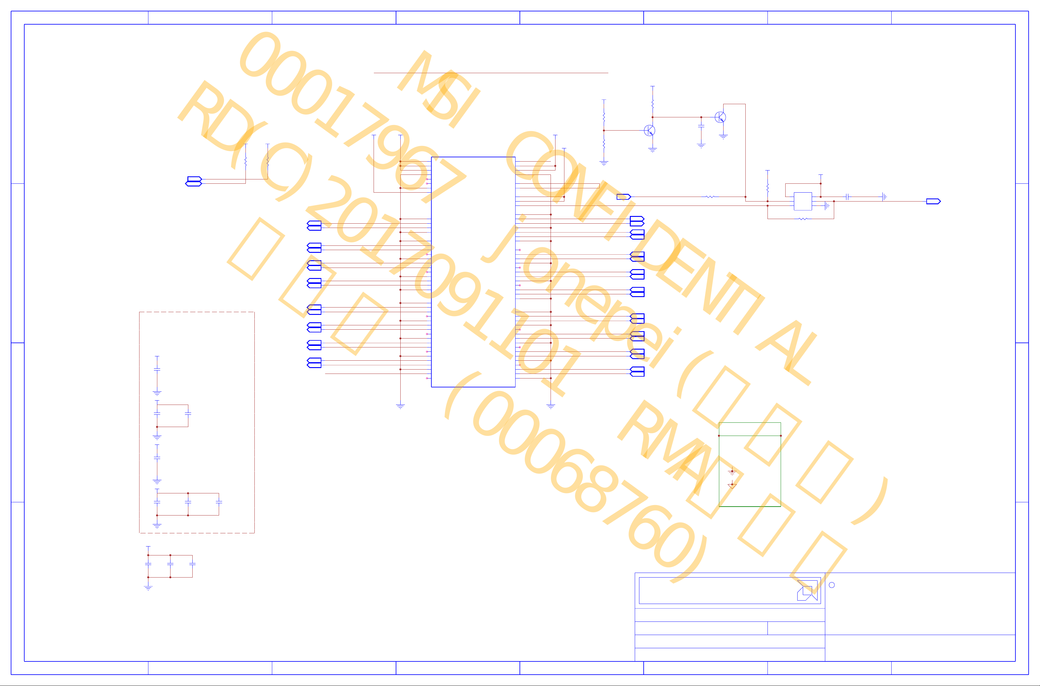
PCI-EXPRESS EDGE CONNECTOR
PCI-EXPRESS EDGE CONNECTOR
+1.8V
+1.8V
PRESENCE
PRESENCE
+12V_BUS
+12V_BUS
+3.3V_BUS
+3.3V_BUS
1
1
JTDIO_LOOP
JTDIO_LOOP
PCIE_REFCLKP
PCIE_REFCLKP
PCIE_REFCLKN
PCIE_REFCLKN
PERP0
PERP0
PERN0
PERN0
PERP1
PERP1
PERN1
PERN1
PERP2
PERP2
PERN2
PERN2
PERP3
PERP3
PERN3
PERN3
PERP4
PERP4
PERN4
PERN4
PERP5
PERP5
PERN5
PERN5
PERP6
PERP6
PERN6
PERN6
PERP7
PERP7
PERN7
PERN7
+12V_BUS+3.3V_BUS
+12V_BUS+3.3V_BUS
+3.3V_BUS
+3.3V_BUS
SMBCLK
IN
BI
SMBCLK
SMBDATA
SMBDATA
5
5
5
5
C
Place these caps as close to the PCIE
Place these caps as close to the PCIE
CAP CER 10UF 20% 16V X5R
CAP CER 10UF 20% 16V X5R
connector as possible
connector as possible
(1206)1.8MM H MAX
(1206)1.8MM H MAX
+12V_BUS
+12V_BUS
1
+12V_BUS
1
+12V_BUS
C1001
C1001
10uF
10uF
16V
16V
2 1
2 1
R1
45.3K
45.3K
1%
1%
2 1
2 1
+3.3V_BUS
+3.3V_BUS
R2
R2R1
45.3K
45.3K
1%
1%
2 1
2 1
MPCIE1
B1
B1
+12V
B2
B2
+12V
B3
B3
+12V
B4
B4
GND
B5
B5
SMCLK
B6
B6
SMDAT
B7
B7
GND
B8
B8
+3.3V
B13
B13
GND
B14
PETP0_GFXRP0
2
2
OUT
2
2
OUT
2
2
OUT
2
2
OUT
2
2
OUT
2
2
OUT
2
2
OUT
2
2
OUT
2
2
OUT
2
2
OUT
2
2
OUT
2
2
OUT
2
2
OUT
2
2
OUT
2
2
OUT
2
2
OUT
1
1
PETP0_GFXRP0
PETN0_GFXRN0
PETN0_GFXRN0
PETP1_GFXRP1
PETP1_GFXRP1
PETN1_GFXRN1
PETN1_GFXRN1
PETP2_GFXRP2
PETP2_GFXRP2
PETN2_GFXRN2
PETN2_GFXRN2
PETP3_GFXRP3
PETP3_GFXRP3
PETN3_GFXRN3
PETN3_GFXRN3
PETP4_GFXRP4
PETP4_GFXRP4
PETN4_GFXRN4
PETN4_GFXRN4
PETP5_GFXRP5
PETP5_GFXRP5
PETN5_GFXRN5
PETN5_GFXRN5
PETP6_GFXRP6
PETP6_GFXRP6
PETN6_GFXRN6
PETN6_GFXRN6
PETP7_GFXRP7
PETP7_GFXRP7
PETN7_GFXRN7
PETN7_GFXRN7
PRESENCE
PRESENCE
B14
B15
B15
B16
B16
B18
B18
B19
B19
B20
B20
B21
B21
B22
B22
B23
B23
B24
B24
B25
B25
B26
B26
B27
B27
B28
B28
B29
B29
B32
B32
B33
B33
B34
B34
B35
B35
B36
B36
B37
B37
B38
B38
B39
B39
B40
B40
B41
B41
B42
B42
B43
B43
B44
B44
B45
B45
B46
B46
B47
B47
B48
B48
B49
B49
PETp0
PETn0
GND
GND
PETp1
PETn1
GND
GND
PETp2
PETn2
GND
GND
PETp3
PETn3
GND
GND
PETp4
PETn4
GND
GND
PETp5
PETn5
GND
GND
PETp6
PETn6
GND
GND
PETp7
PETn7
GND
PRSNT2_B48
GND
MPCIE1
Mechanical Key
PRSNT1_A1
+12V
+12V
GND
JTAG3
JTAG4
+3.3V
+3.3V
PERST_
GND
REFCLK+
REFCLK-
GND
PERp0
PERn0
GND
GND
PERp1
PERn1
GND
GND
PERp2
PERn2
GND
GND
PERp3
PERn3
GND
GND
PERp4
PERn4
GND
GND
PERp5
PERn5
GND
GND
PERp6
PERn6
GND
GND
PERp7
PERn7
GND
A1
A1
A2
A2
A3
A3
A4
A4
A6
A6
A7
A7
A9
A9
A10
A10
A11
A11
A12
A12
A13
A13
A14
A14
A15
A15
A16
A16
A17
A17
A18
A18
A20
A20
A21
A21
A22
A22
A23
A23
A24
A24
A25
A25
A26
A26
A27
A27
A28
A28
A29
A29
A30
A30
A31
A31
A34
A34
A35
A35
A36
A36
A37
A37
A38
A38
A39
A39
A40
A40
A41
A41
A42
A42
A43
A43
A44
A44
A45
A45
A46
A46
A47
A47
A48
A48
A49
A49
R3
R3
10K
10K
1%
1%
DNI
DNI
2 1
2 1
1.8V_IN
1.8V_IN
R4
R4
10K
10K
DNI
DNI
2 1
2 1
15 14
15 14
IN
OUT
OUT
IN
IN
IN
IN
IN
IN
IN
IN
IN
IN
IN
IN
IN
IN
IN
IN
2
2
+3.3V_BUS
+3.3V_BUS
2 11 6
2 1
1 6
+1.8V_EN
+1.8V_EN
2
2
2
2
2
2
2
2
2
2
2
2
2
2
2
2
2
2
2
2
2
2
2
2
2
2
2
2
2
2
2
2
2
2
2
2
R50
R50
10K
10K
1%
1%
DNI
DNI
Q1
Q1
MMDT3904-7
MMDT3904-7
DNI
DNI
PWR_IN
PWR_IN
R23
C50
C50
0.1uF
0.1uF
10V
10V
2 1
2 1
DNI
DNI
PWR_RST
PWR_RST
5
5
Q1
Q1
MMDT3904-7
MMDT3904-7
DNI
DNI
4 3
4 3
0R
0R
21R23
21
PERST#
PERST#
+3.3V_BUS
+3.3V_BUS
21
21
10K
10K
R1005
R1005
DNI
DNI
U4
U4
3
3
A
1
1
B
C
74AUP1G57GM
74AUP1G57GM
R1007
Place R1007 in U4
Place R1007 in U4
+3.3V_BUS
+3.3V_BUS
VCC
Y
GND
21R1007
21
6.3V
0.1uF
0.1uF
6.3V
PERST#_BUF
PERST#_BUF
OUT
2 16
2 16
5
C1011
5
4
4
26
26
0RDNI
0RDNI
21C1011
21
DD
C
A
+12V_BUS
+12V_BUS
1
+12V_BUS
1
+12V_BUS
C1002
0.15uF
0.15uF
16V
16V
2 1
2 12 1
+3.3V_BUS
+3.3V_BUS
+3.3V_BUS
1
+3.3V_BUS
1
C1004
C1004
10uF
10uF
6.3V
6.3V
2 1
+3.3V_BUS
+3.3V_BUS
1
+3.3V_BUS
1
+3.3V_BUS
C1005
C1005
0.1uF
0.1uF
6.3V
6.3V
2 1
2 1
+12V_BUS
+12V_BUS
+12V_BUS
1
+12V_BUS
1
C1008
C1008
0.1uF
0.1uF
16V
16V
2 1
2 1
2 1
2 1
8
C1003
C1003C1002
0.15uF
0.15uF
16V
16V
2 1
2 1
CAP CER 10UF 10% 6.3V X5R
CAP CER 10UF 10% 6.3V X5R
(0805)1.4MM MAX THICK
(0805)1.4MM MAX THICK
21
21
C1006
1uF
1uF
6.3V
C1009
0.1uF
0.1uF
16V
16V
6.3V
2 1
2 1
C1010
C1010C1009
0.1uF
0.1uF
16V
16V
2 1
2 1
7
C1007
C1007C1006
0.01uF
0.01uF
10V
10V
6
x8 PCIe
x8 PCIe
SYMBOL LEGEND
SYMBOL LEGEND
DNI
DNI
BUO
BUO
AMD - PLATFORM HARDWARE ENG
AMD - PLATFORM HARDWARE ENG
#48, No.1387, ZHANGDONG ROAD
#48, No.1387, ZHANGDONG ROAD
SHANGHAI, CHINA 201203
SHANGHAI, CHINA 201203
SHEET:
DATE:
SHEET NUMBER:
DOCUMENT NUMBER:
5
4
PCI-E Edge Connector
PCI-E Edge Connector
Fri Oct 28 17:09:42 2016
Fri Oct 28 17:09:42 2016 1.0
1 21
1 21
OF
105_CXXX00_00A
105_CXXX00_00A
3
DO NOT
DO NOT
INSTALL
INSTALL
# ACTIVE
# ACTIVE
LOW
LOW
DIGITAL
DIGITAL
GROUND
GROUND
ANALOG
ANALOG
GROUND
GROUND
BRING UP
BRING UP
ONLY
ONLY
REV:
1.0
CONFIDENTIAL AND PROPRIETARY TO ADVANCED MICRO DEVICES INC.
2016
2016
C
This AMD Board schematic and design is the exclusive property of AMD, and
is provided only to entities under a non-disclosure agreement with AMD
for evaluation purposes. Further distribution or disclosure is strictly
prohibited. Use of this schematic and design for any purpose other than
evaluation requires a Board Technology License Agreement with AMD.
AMD makes no representations or warranties of any kind regarding this
schematic and design, including, not limited to, any implied warranty
of merchantability or fitness for a particular purpose, and disclaims
responsibility for any consequences resulting from use of the
information included herein.
TITLE:
2
Advanced Micro Devices
TITLE
TITLE
1
BB
A
Page 2
This AMD Board schematic and design is the exclusive property of AMD, and
DATE:
SHEET:
Advanced Micro Devices
2
3
345
6
6
7
7
8
8
C
5
CONFIDENTIAL AND PROPRIETARY TO ADVANCED MICRO DEVICES INC.
C
BB
A
1
DD
C
A
4
REV:
SHEET NUMBER:
DOCUMENT NUMBER:
OF
1
prohibited. Use of this schematic and design for any purpose other than
for evaluation purposes. Further distribution or disclosure is strictly
is provided only to entities under a non-disclosure agreement with AMD
2
schematic and design, including, not limited to, any implied warranty
AMD makes no representations or warranties of any kind regarding this
evaluation requires a Board Technology License Agreement with AMD.
of merchantability or fitness for a particular purpose, and disclaims
responsibility for any consequences resulting from use of the
information included herein.
TITLE:
INININININININININININ
VSS
VSS
VSS
VSS
VSS
VSS
VSS
VSS
VSS
VSS
VSS
VSS
VSS
VSS
VSS
VSS
VSS
VSS
VSS
VSS
VSS
VSS
VSS
VSS
VSS
VSS
VSS
VSS
VSS
VSS
VSS
VSS
VSS
VSS
VSSPX_EN
PERSTB
PCIE_VDDC
PCIE_VDDC
PCIE_VDDC
PCIE_VDDC
PCIE_VDDC
PCIE_VDDC
PCIE_VDDC
PCIE_VDDC
PCIE_VDDC
PCIE_VDDC
PCIE_VDDC
NC#N30
NC#N29
NC#N33
NC#N32
PCIE_TX7P
PCIE_TX7N
PCIE_TX6P
PCIE_TX6N
PCIE_TX5P
PCIE_TX5N
PCIE_TX4P
PCIE_TX4N
PCIE_TX3P
PCIE_TX3N
PCIE_TX2P
PCIE_TX2N
PCIE_TX1P
PCIE_TX1N
NC#H33
NC#H32
NC#K30
NC#K29
NC#J33
NC#J32
NC#K33
NC#K32
NC#L30
NC#L29
NC#L33
NC#L32
PCIE_TX0P
PCIE_TX0N
NC#M35
NC#L36
NC#N38
NC#M37
PCIE_RX7P
PCIE_RX7N
PCIE_RX6P
PCIE_RX6N
PCIE_RX5P
PCIE_RX5N
PCIE_RX4P
PCIE_RX4N
PCIE_RX3P
PCIE_RX3N
PCIE_RX2P
PCIE_RX2N
PCIE_RX1P
PCIE_RX1N
NC#F35
NC#E37
NC#G38
NC#F37
NC#H35
NC#G36
NC#J38
NC#H37
NC#K35
NC#J36
NC#L38
NC#K37
PCIE_RX0P
PCIE_RX0N
PCIE_REFCLKP
PCIE_REFCLKN
PCIE_PVDD
PCIE_CALR_TX
PCIE_CALR_RX
NC_BIF_VDDC
NC_BIF_VDDC
NC#38
NC#37
NC#36
NC#35
NC#34
NC#33
PCIE_VDDC
OUT
OUT
OUT
OUT
OUT
OUT
OUT
OUT
OUT
OUT
OUT
OUT
OUT
OUT
OUT
OUTININININININININ
8
MSI CONFIDENTIAL
00017967 jonepei(裴亮樂)
RD(C)2017091101 RMA工程課
石阿鋒 (00068760)
7
6
345
2
1
C
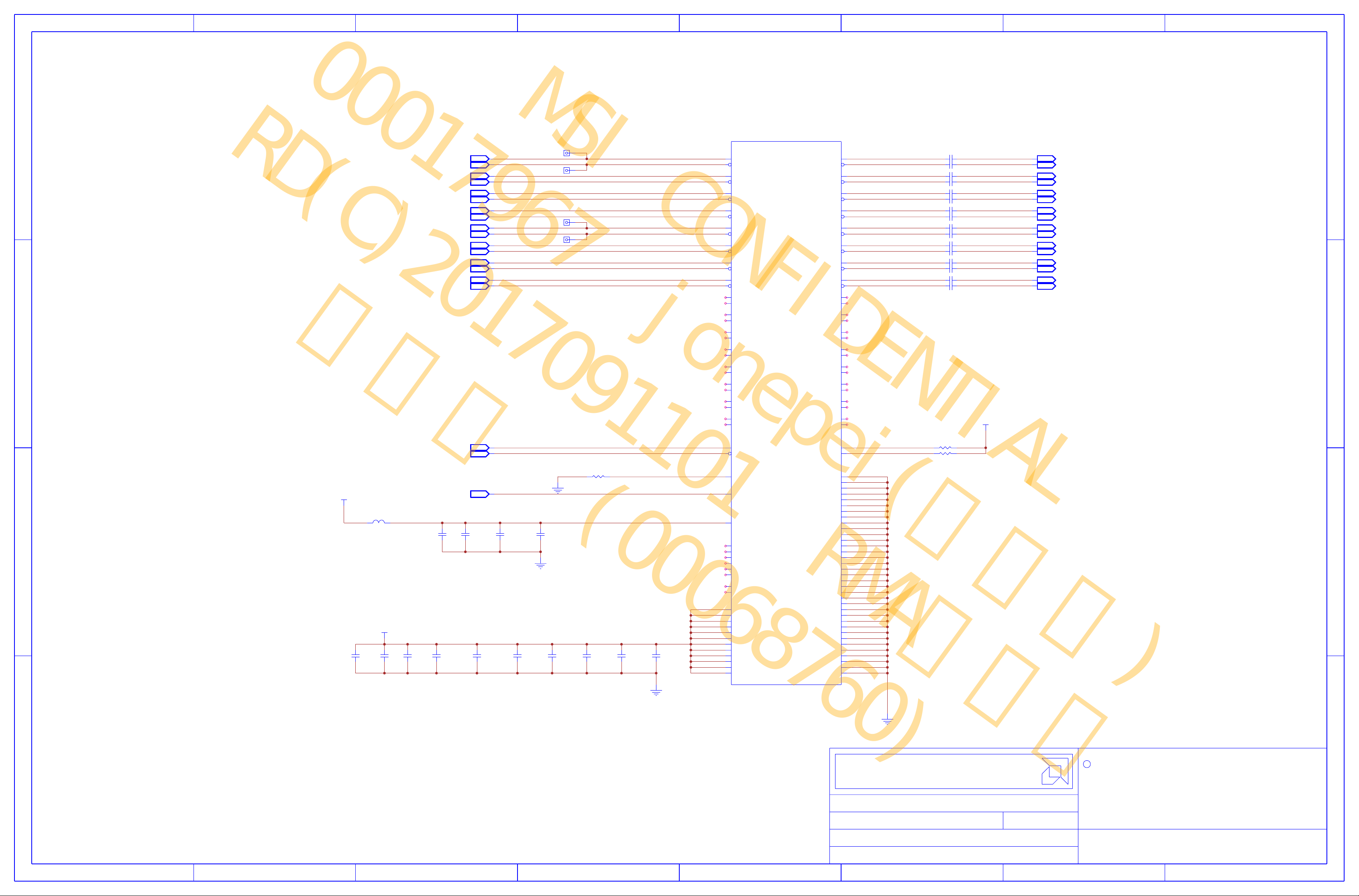
Oland PCIe Interface
Oland PCIe Interface
+1.8V
+1.8V
2 1
2 1
C1161
1uF
1uF
6.3V
6.3V
B11
B11
+0.95V
+0.95V
120R
120R
2 1
2 1
21
21
C1160
10uF
10uF
6.3V
6.3V
PCIE_TX0P
PCIE_TX0P
PCIE_TX0N
PCIE_TX0N
PCIE_TX1P
PCIE_TX1P
PCIE_TX1N
PCIE_TX1N
PCIE_TX2P
PCIE_TX2P
PCIE_TX2N
PCIE_TX2N
PCIE_TX3P
PCIE_TX3P
PCIE_TX3N
PCIE_TX3N
PCIE_TX4P
PCIE_TX4P
PCIE_TX4N
PCIE_TX4N
PCIE_TX5P
PCIE_TX5P
PCIE_TX5N
PCIE_TX5N
PCIE_TX6P
PCIE_TX6P
PCIE_TX6N
PCIE_TX6N
PCIE_TX7P
PCIE_TX7P
PCIE_TX7N
PCIE_TX7N
R1013
R1014
C1101
C1102
C1103
C1104
C1105
C1106
C1107
C1108
C1109
C1110
C1111
C1112
C1113
C1114
C1115
C1116
220nF for GEN3
220nF for GEN3
21C1101
21
0.22uF
0.22uF
21C1102
21
0.22uF
0.22uF
21C1103
21
0.22uF
0.22uF
21C1104
21
0.22uF
0.22uF
21C1105
21
0.22uF
0.22uF
21C1106
21
0.22uF
0.22uF
21C1107
21
0.22uF
0.22uF
21C1108
21
0.22uF
0.22uF
21C1109
21
0.22uF
0.22uF
21C1110
21
0.22uF
0.22uF
21C1111
21
0.22uF
0.22uF
21C1112
21
0.22uF
0.22uF
21C1113
21
0.22uF
0.22uF
21C1114
21
0.22uF
0.22uF
21C1115
21
0.22uF
0.22uF
21C1116
21
0.22uF
0.22uF
+0.95V
+0.95V
21R1013
21
21R1014
21
10V
10V
10V
10V
10V
10V
10V
10V
10V
10V
10V
10V
10V
10V
10V
10V
10V
10V
10V
10V
10V
10V
10V
10V
10V
10V
10V
10V
10V
10V
10V
10V
1%1.69K
1%1.69K
1%1K
1%1K
1
1
IN
1
1
IN
1
1
IN
1
1
IN
1
1
IN
1
1
IN
1
1
IN
1
1
IN
1
1
IN
1
1
IN
1
1
IN
1
1
IN
1
1
IN
1
1
IN
1
1
IN
1
1
IN
1
1
IN
1
1
IN
17 1
17 1
IN
+PCIE_PVDD
+PCIE_PVDD
2 1
2 1
C1159
10uF
10uF
6.3V
6.3V
C1143
C1143U1C1189
10uF
10uF
6.3V
6.3V
2 1
2 1
C1158
C1158C1159C1161 C1160
10uF
10uF
6.3V
6.3V
2 1
2 1
C1189
1uF
1uF
6.3V
6.3V
2 1
2 1
2 1
2 1
C1150
C1150
1uF
1uF
6.3V
6.3V
2 1
2 1
C1173
C1173
1uF
1uF
6.3V
6.3V
2 1
2 1
C1151
C1151
1uF
1uF
6.3V
6.3V
2 1
2 1
NOTE: Some of the PCIE testpoints will
NOTE: Some of the PCIE testpoints will
be available through vias on traces.
be available through vias on traces.
TP110
TP110
TP109
TP109
TP107
TP107
TP108
TP108
C1175
C1175
0.1uF
0.1uF
6.3V
6.3V
2 1
2 1
R1015
C1152
1uF
1uF
6.3V
6.3V
1K
DNI
21R1015
DNI
1K
21
PERST#_BUF
PERST#_BUF
1.8V 200mA
1.8V 200mA
C1153
C1153C1152
1uF
1uF
6.3V
6.3V
2 1
2 1
2 1
2 1
PETP1_GFXRP1
PETP1_GFXRP1
PETN1_GFXRN1
PETN1_GFXRN1
PETP3_GFXRP3
PETP3_GFXRP3
PETN3_GFXRN3
PETN3_GFXRN3
PETP4_GFXRP4
PETP4_GFXRP4
PETN4_GFXRN4
PETN4_GFXRN4
PETP5_GFXRP5
PETP5_GFXRP5
PETN5_GFXRN5
PETN5_GFXRN5
PETP7_GFXRP7
PETP7_GFXRP7
PETN7_GFXRN7
PETN7_GFXRN7
PCIE_REFCLKN PCIE_CALRN
PCIE_REFCLKN PCIE_CALRN
C1154
C1154
1uF
1uF
6.3V
6.3V
PETP0_GFXRP0
PETP0_GFXRP0
PETN0_GFXRN0
PETN0_GFXRN0
PETP2_GFXRP2
PETP2_GFXRP2
PETN2_GFXRN2
PETN2_GFXRN2
PETP6_GFXRP6
PETP6_GFXRP6
PETN6_GFXRN6
PETN6_GFXRN6
PX_EN
PX_EN
C1155
C1155
1uF
1uF
6.3V
6.3V
2 1
2 1
U1
AA38
AA38
PCIE_RX0P
Y37
Y37
PCIE_RX0N
Y35
Y35
PCIE_RX1P
W36
W36
PCIE_RX1N
W38
W38
PCIE_RX2P
V37
V37
PCIE_RX2N
V35
V35
PCIE_RX3P
U36
U36
PCIE_RX3N
U38
U38
PCIE_RX4P
T37
T37
PCIE_RX4N
T35
T35
PCIE_RX5P
R36
R36
PCIE_RX5N
R38
R38
PCIE_RX6P
P37
P37
PCIE_RX6N
P35
P35
PCIE_RX7P
N36
N36
PCIE_RX7N
N38 N33
N38 N33
NC#N38
M37
M37
NC#M37
M35
M35
NC#M35
L36
L36
NC#L36
L38
L38
NC#L38
K37
K37
NC#K37
K35
K35
NC#K35
J36
J36
NC#J36
J38
J38
NC#J38
H37
H37
NC#H37
H35
H35
NC#H35
G36
G36
NC#G36
G38
G38
NC#G38
F37
F37
NC#F37
F35
F35
NC#F35
E37
E37
NC#E37
AB35
AB35
PCIE_REFCLKP
AA36
AA36
PCIE_REFCLKN
AA30
AA30
PERSTB
AB37
AB37
PCIE_PVDD
AA31
AA31
NC#33
AA32
AA32
NC#34
AA33
AA33
NC#35
AA34
AA34
NC#36
W30
W30
NC#37
Y31
Y31
NC#38
V28
V28
NC_BIF_VDDC
W29
W29
NC_BIF_VDDC
G30
G30
PCIE_VDDC
G31
G31
PCIE_VDDC
H29
H29
PCIE_VDDC
H30
H30
PCIE_VDDC
J29
J29
PCIE_VDDC
J30
J30
PCIE_VDDC
L28
L28
PCIE_VDDC
M28
M28
PCIE_VDDC
N28
N28
PCIE_VDDC
R28
R28
PCIE_VDDC
T28
T28
PCIE_VDDC
U28
U28
PCIE_VDDC
PCIE_TX0P
PCIE_TX0N
PCIE_TX1P
PCIE_TX1N
PCIE_TX2P
PCIE_TX2N
PCIE_TX3P
PCIE_TX3N
PCIE_TX4P
PCIE_TX4N
PCIE_TX5P
PCIE_TX5N
PCIE_TX6P
PCIE_TX6N
PCIE_TX7P
PCIE_TX7N
NC#N33
NC#N32
NC#N30
NC#N29
NC#L33
NC#L32
NC#L30
NC#L29
NC#K33
NC#K32
NC#J33
NC#J32
NC#K30
NC#K29
NC#H33
NC#H32
PCIE_CALR_TX
PCIE_CALR_RX
VSSPX_EN
VSS
VSS
VSS
VSS
VSS
VSS
VSS
VSS
VSS
VSS
VSS
VSS
VSS
VSS
VSS
VSS
VSS
VSS
VSS
VSS
VSS
VSS
VSS
VSS
VSS
VSS
VSS
VSS
VSS
VSS
VSS
VSS
VSS
VSS
Y33
Y33
Y32
Y32
W33
W33
W32
W32
U33
U33
U32
U32
U30
U30
U29
U29
T33
T33
T32
T32
T30
T30
T29
T29
P33
P33
P32
P32
P30
P30
P29
P29
N32
N32
N30
N30
N29
N29
L33
L33
L32
L32
L30
L30
L29
L29
K33
K33
K32
K32
J33
J33
J32
J32
K30
K30
K29
K29
H33
H33
H32
H32
Y30
Y30
Y29
Y29
AB39AL21
AB39AL21
E39
E39
F34
F34
F39
F39
G33
G33
G34
G34
H31
H31
H34
H34
H39
H39
J31
J31
J34
J34
K31
K31
K34
K34
K39
K39
L31
L31
L34
L34
M34
M34
M39
M39
N31
N31
N34
N34
P31
P31
P34
P34
P39
P39
R34
R34
T31
T31
T34
T34
T39
T39
U31
U31
U34
U34
V34
V34
Y39
Y39
V39
V39
W31
W31
W34
W34
Y34
Y34
PCIE_CALRPPCIE_REFCLKP
PCIE_CALRPPCIE_REFCLKP
PERP0
PERP0
PERN0
PERN0
PERP1
PERP1
PERN1
PERN1
PERP2
PERP2
PERN2
PERN2
PERP3
PERP3
PERN3
PERN3
PERP4
PERP4
PERN4
PERN4
PERP5
PERP5
PERN5
PERN5
PERP6
PERP6
PERN6
PERN6
PERP7
PERP7
PERN7
PERN7
PCIE_CALR_TX 1.69k pull up for Oland
PCIE_CALR_TX 1.69k pull up for Oland
PCIE_CALR_RX 1k pull up for Oland
PCIE_CALR_RX 1k pull up for Oland
OUT
OUT
OUT
OUT
OUT
OUT
OUT
OUT
OUT
OUT
OUT
OUT
OUT
OUT
OUT
OUT
1
1
1
1
1
1
1
1
1
1
1
1
1
1
1
1
1
1
1
1
1
1
1
1
1
1
1
1
1
1
1
1
DD
C
BB
A
8
7
6
5
4
OLAND M2 GDDR5
OLAND M2 GDDR5
AMD - PLATFORM HARDWARE ENG
AMD - PLATFORM HARDWARE ENG
#48, No.1387, ZHANGDONG ROAD
#48, No.1387, ZHANGDONG ROAD
SHANGHAI, CHINA 201203
SHANGHAI, CHINA 201203
SHEET:
DATE:
SHEET NUMBER:
DOCUMENT NUMBER:
Oland PCIE Interface
Oland PCIE Interface
Fri Oct 28 17:09:40 2016
Fri Oct 28 17:09:40 2016 1.0
2 21
2 21
OF
105_CXXX00_00A
105_CXXX00_00A
3
REV:
1.0
CONFIDENTIAL AND PROPRIETARY TO ADVANCED MICRO DEVICES INC.
2016
2016
C
This AMD Board schematic and design is the exclusive property of AMD, and
is provided only to entities under a non-disclosure agreement with AMD
for evaluation purposes. Further distribution or disclosure is strictly
prohibited. Use of this schematic and design for any purpose other than
evaluation requires a Board Technology License Agreement with AMD.
AMD makes no representations or warranties of any kind regarding this
schematic and design, including, not limited to, any implied warranty
of merchantability or fitness for a particular purpose, and disclaims
responsibility for any consequences resulting from use of the
information included herein.
TITLE:
2
Advanced Micro Devices
TITLE
TITLE
1
A
Page 3
This AMD Board schematic and design is the exclusive property of AMD, and
DATE:
SHEET:
Advanced Micro Devices
2
3
345
6
6
7
7
8
8
C
5
CONFIDENTIAL AND PROPRIETARY TO ADVANCED MICRO DEVICES INC.
C
BB
A
1
DD
C
A
4
REV:
SHEET NUMBER:
DOCUMENT NUMBER:
OF
1
prohibited. Use of this schematic and design for any purpose other than
for evaluation purposes. Further distribution or disclosure is strictly
is provided only to entities under a non-disclosure agreement with AMD
2
schematic and design, including, not limited to, any implied warranty
AMD makes no representations or warranties of any kind regarding this
evaluation requires a Board Technology License Agreement with AMD.
of merchantability or fitness for a particular purpose, and disclaims
responsibility for any consequences resulting from use of the
information included herein.
TITLE:
WEB1BWEB0B
WCKB1B_1
WCKB1B_0
WCKB1_1
WCKB1_0
WCKB0B_1
WCKB0B_0
WCKB0_1
WCKB0_0
RASB1BRASB0B
MVREFSB
MVREFDB
MEM_CALRP0
MAB1_9
MAB1_8
MAB1_7
MAB1_6
MAB1_5
MAB1_4
MAB1_3
MAB1_2
MAB1_1
MAB1_0
MAB0_9
MAB0_8
MAB0_7
MAB0_6
MAB0_5
MAB0_4
MAB0_3
MAB0_2
MAB0_1
MAB0_0
EDCB1_3
EDCB1_2
EDCB1_1
EDCB1_0
EDCB0_3
EDCB0_2
EDCB0_1
EDCB0_0
DQB1_9
DQB1_8
DQB1_7
DQB1_6
DQB1_5
DQB1_4
DQB1_31
DQB1_30
DQB1_3
DQB1_29
DQB1_28
DQB1_27
DQB1_26
DQB1_25
DQB1_24
DQB1_23
DQB1_22
DQB1_21
DQB1_20
DQB1_2
DQB1_19
DQB1_18
DQB1_17
DQB1_16
DQB1_15
DQB1_14
DQB1_13
DQB1_12
DQB1_11
DQB1_10
DQB1_1
DQB1_0
DQB0_9
DQB0_8
DQB0_7
DQB0_6
DQB0_5
DQB0_4
DQB0_31
DQB0_30
DQB0_3
DQB0_29
DQB0_28
DQB0_27
DQB0_26
DQB0_25
DQB0_24
DQB0_23
DQB0_22
DQB0_21
DQB0_20
DQB0_2
DQB0_19
DQB0_18
DQB0_17
DQB0_16
DQB0_15
DQB0_14
DQB0_13
DQB0_12
DQB0_11
DQB0_10
DQB0_1
DQB0_0
DDBIB1_3
DDBIB1_2
DDBIB1_1
DDBIB1_0
DDBIB0_3
DDBIB0_2
DDBIB0_1
DDBIB0_0
CSB1B_1
CSB1B_0
CSB0B_1
CSB0B_0
CLKB1B
CLKB1
CLKB0B
CLKB0
CKEB1CKEB0
CASB1BCASB0B
ADBIB1ADBIB0
WEA1BWEA0B
WCKA1B_1
WCKA1B_0
WCKA1_1
WCKA1_0
WCKA0B_1
WCKA0B_0
WCKA0_1
WCKA0_0
RASA1BRASA0B
MVREFSA
MVREFDA
MAA1_9
MAA1_8
MAA1_7
MAA1_6
MAA1_5
MAA1_4
MAA1_3
MAA1_2
MAA1_1
MAA1_0
MAA0_9
MAA0_8
MAA0_7
MAA0_6
MAA0_5
MAA0_4
MAA0_3
MAA0_2
MAA0_1
MAA0_0
EDCA1_3
EDCA1_2
EDCA1_1
EDCA1_0
EDCA0_3
EDCA0_2
EDCA0_1
EDCA0_0
DRAM_RST
DQA1_9
DQA1_8
DQA1_7
DQA1_6
DQA1_5
DQA1_4
DQA1_31
DQA1_30
DQA1_3
DQA1_29
DQA1_28
DQA1_27
DQA1_26
DQA1_25
DQA1_24
DQA1_23
DQA1_22
DQA1_21
DQA1_20
DQA1_2
DQA1_19
DQA1_18
DQA1_17
DQA1_16
DQA1_15
DQA1_14
DQA1_13
DQA1_12
DQA1_11
DQA1_10
DQA1_1
DQA1_0
DQA0_9
DQA0_8
DQA0_7
DQA0_6
DQA0_5
DQA0_4
DQA0_31
DQA0_30
DQA0_3
DQA0_29
DQA0_28
DQA0_27
DQA0_26
DQA0_25
DQA0_24
DQA0_23
DQA0_22
DQA0_21
DQA0_20
DQA0_2
DQA0_19
DQA0_18
DQA0_17
DQA0_16
DQA0_15
DQA0_14
DQA0_13
DQA0_12
DQA0_11
DQA0_10
DQA0_1
DQA0_0
DDBIA1_3
DDBIA1_2
DDBIA1_1
DDBIA1_0
DDBIA0_3
DDBIA0_2
DDBIA0_1
DDBIA0_0
CSA1B_1
CSA1B_0
CSA0B_1
CSA0B_0
CLKA1B
CLKA1
CLKA0B
CLKA0
CKEA1CKEA0
CASA1BCASA0B
ADBIA1ADBIA0
OUT
OUT
OUT
OUT
OUT
OUT
OUT
OUTBIBIBIBIBIBIBIBIBIBIBIBIBIOUT
OUT
OUT
OUT
OUT
OUT
OUTBIBIBIBIBIBIBIBIBIBIBIBI
BI
OUT
OUT
OUT
OUT
OUT
OUT
OUTBIBIBIBIBIBIBIBIBIBIBIBIBIOUT
OUT
OUT
OUT
OUT
OUT
OUTBIBIBIBIBIBIBIBIBIBIBIBIBIOUT
OUT
OUT
OUTBIBIBIBI
8
MSI CONFIDENTIAL
00017967 jonepei(裴亮樂)
RD(C)2017091101 RMA工程課
石阿鋒 (00068760)
7
6
345
2
1
C
A
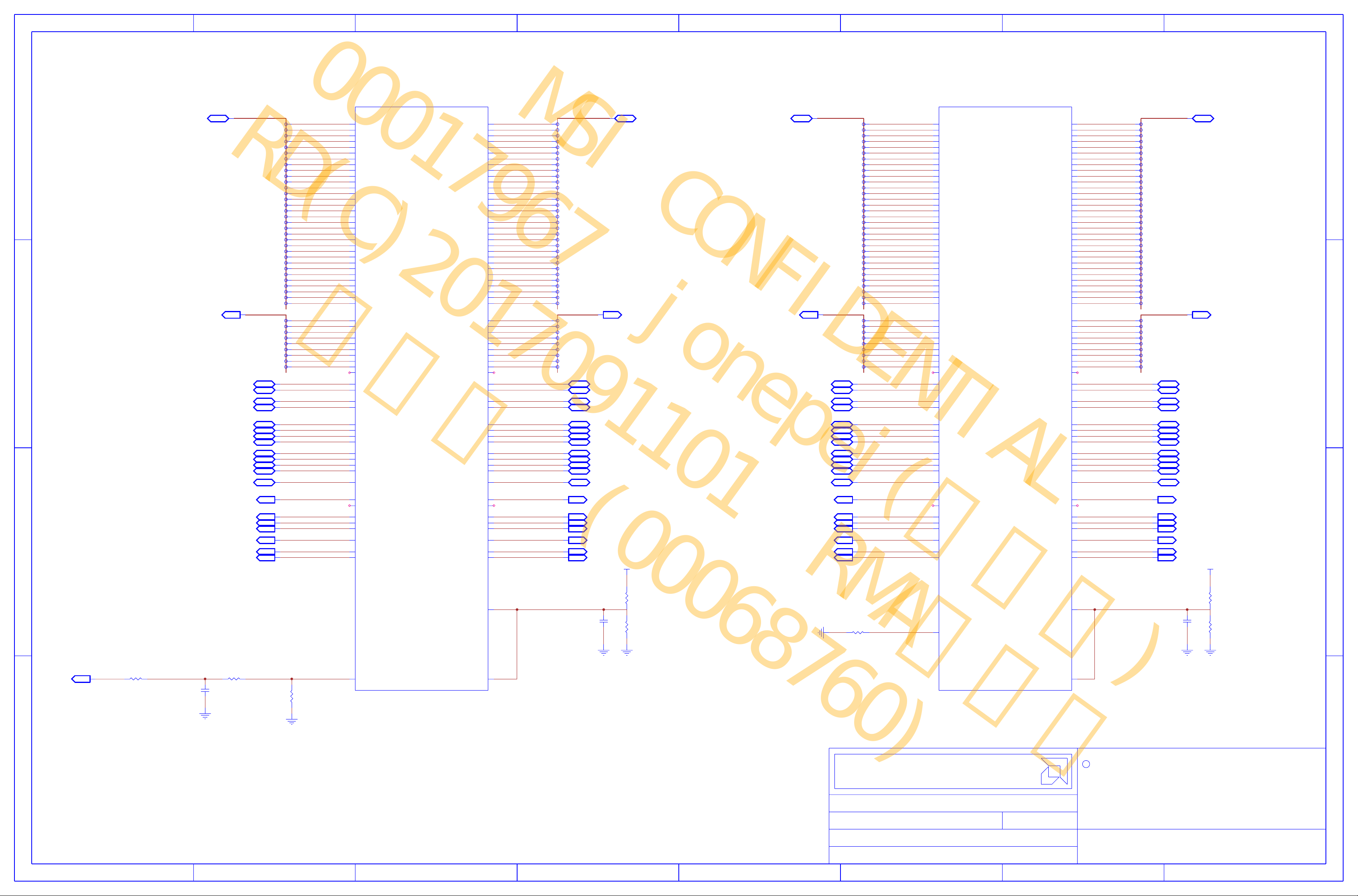
(3) Oland MEM Interface Ch A&B
(3) Oland MEM Interface Ch A&B
U1
DQA0_<31..0>
3 4 3 4 3 4 3 4
3 4 3 4 3 4 3 4
3 4
3 4
DRAM_RST DRAM_RST_RR
4
4
DRAM_RST DRAM_RST_RR
OUT
R3630
R3630
49.9R
49.9R
1%
1%
21
21
C3607
C3607
120pF
120pF
50V
50V
2 1
2 1
DQA0_<31..0>
4
4
BI
4
4
BI
4
4
BI
4
4
BI
4
4
BI
4
4
BI
4
4
BI
4
4
BI
4
4
BI
4
4
BI
4
4
BI
4
4
BI
4
4
BI
4
4
OUT
4
4
OUT
4
4
OUT
4
4
OUT
4
4
OUT
4
4
OUT
4
4
OUT
21
21
R3615
R3615
10R
10R
1%
1%
0
0
4 3
4 3
1
1
4 3
4 3
2
2
4 3
4 3
3
3
4 3
4 3
4
4
4 3
4 3
5
5
4 3
4 3
6
6
4 3
4 3
7
7
4 3
4 3
8
8
4 3
4 3
9
9
4 3
4 3
10
10
4 3
4 3
11
11
4 3
4 3
12
12
4 3
4 3
13
13
4 3
4 3
14
14
4 3
4 3
15
15
4 3
4 3
16
16
4 3
4 3
17
17
4 3
4 3
18
18
4 3
4 3
19
19
4 3
4 3
20
20
4 3
4 3
21
21
4 3
4 3
22
22
4 3
4 3
23
23
4 3
4 3
24
24
4 3
4 3
25
25
4 3
4 3
26
26
4 3
4 3
27
27
4 3
4 3
28
28
4 3
4 3
29
29
4 3
4 3
30
30
4 3
4 3
31
31
0
0
4 3
4 3
1
1
4 3
4 3
2
2
4 3
4 3
3
3
4 3
4 3
4
4
4 3
4 3
5
5
4 3
4 3
6
6
4 3
4 3
7
7
4 3
4 3
8
8
DRAM_RST_R
DRAM_RST_R
21
21
4
4
DQA0_<0>
DQA0_<0>
3
3
DQA0_<1>
DQA0_<1>
DQA0_<2>
DQA0_<2>
DQA0_<3>
DQA0_<3>
DQA0_<4>
DQA0_<4>
DQA0_<5>
DQA0_<5>
DQA0_<6>
DQA0_<6>
DQA0_<7>
DQA0_<7>
DQA0_<8>
DQA0_<8>
DQA0_<9>
DQA0_<9>
DQA0_<10>
DQA0_<10>
DQA0_<11>
DQA0_<11>
DQA0_<12>
DQA0_<12>
DQA0_<13>
DQA0_<13>
DQA0_<14>
DQA0_<14>
DQA0_<15>
DQA0_<15>
DQA0_<16>
DQA0_<16>
DQA0_<17>
DQA0_<17>
DQA0_<18>
DQA0_<18>
DQA0_<19>
DQA0_<19>
DQA0_<20>
DQA0_<20>
DQA0_<21>
DQA0_<21>
DQA0_<22>
DQA0_<22>
DQA0_<23>
DQA0_<23>
DQA0_<24>
DQA0_<24>
DQA0_<25>
DQA0_<25>
DQA0_<26>
DQA0_<26>
DQA0_<27>
DQA0_<27>
DQA0_<28>
DQA0_<28>
DQA0_<29>
DQA0_<29>
DQA0_<30>
DQA0_<30>
DQA0_<31>
DQA0_<31>
4
4
3
3
MAA0_<0>
MAA0_<0>
MAA0_<1>
MAA0_<1>
MAA0_<2>
MAA0_<2>
MAA0_<3>
MAA0_<3>
MAA0_<4>
MAA0_<4>
MAA0_<5>
MAA0_<5>
MAA0_<6>
MAA0_<6>
MAA0_<7>
MAA0_<7>
MAA0_<8>
MAA0_<8>
WCKA0_0
WCKA0_0
WCKA0B_0
WCKA0B_0
WCKA0_1
WCKA0_1
WCKA0B_1
WCKA0B_1
EDCA0_0
EDCA0_0
EDCA0_1
EDCA0_1
EDCA0_2
EDCA0_2
EDCA0_3
EDCA0_3
DDBIA0_1
DDBIA0_1
DDBIA0_2
DDBIA0_2
DDBIA0_3
DDBIA0_3
ADBIA0 ADBIA1
ADBIA0 ADBIA1
CSA0B_0
CSA0B_0
CASA0B
CASA0B
RASA0B
RASA0B
WEA0B
WEA0B
CKEA0 CKEA1
CKEA0 CKEA1
CLKA0 CLKA1
CLKA0 CLKA1
CLKA0B
CLKA0B
R3612
R3612
5.1K
5.1K
1%
1%
C37
C37
C35
C35
A35
A35
E34
E34
G32
G32
D33
D33
F32
F32
E32
E32
D31
D31
F30
F30
C30
C30
A30
A30
F28
F28
C28
C28
A28
A28
E28
E28
D27
D27
F26
F26
C26
C26
A26
A26
F24
F24
C24
C24
A24
A24
E24
E24
C22
C22
A22
A22
F22
F22
D21
D21
A20
A20
F20
F20
D19
D19
E18
E18
G24
G24
J23
J23
H24
H24
J24
J24
H26
H26
J26
J26
H21
H21
G21
G21
H23
H23
M21
M21
A32
A32
C32
C32
D23
D23
E22
E22
C34
C34
D29
D29
D25
D25
E20
E20
A34
A34
E30
E30
E26
E26
C20
C20
K24
K24
K27
K27
H27
H27
G27
G27
AH11
AH11
DQA0_0
DQA0_1
DQA0_2
DQA0_3
DQA0_4
DQA0_5
DQA0_6
DQA0_7
DQA0_8
DQA0_9
DQA0_10
DQA0_11
DQA0_12
DQA0_13
DQA0_14
DQA0_15
DQA0_16
DQA0_17
DQA0_18
DQA0_19
DQA0_20
DQA0_21
DQA0_22
DQA0_23
DQA0_24
DQA0_25
DQA0_26
DQA0_27
DQA0_28
DQA0_29
DQA0_30
DQA0_31
MAA0_0
MAA0_1
MAA0_2
MAA0_3
MAA0_4
MAA0_5
MAA0_6
MAA0_7
MAA0_8
MAA0_9
WCKA0_0
WCKA0B_0
WCKA0_1
WCKA0B_1
EDCA0_0
EDCA0_1
EDCA0_2
EDCA0_3
DDBIA0_0
DDBIA0_1
DDBIA0_2
DDBIA0_3
CSA0B_0
CSA0B_1
CLKA0
CLKA0B
DRAM_RST
OLAND M2 GDDR5
OLAND M2 GDDR5
DQA1_0
DQA1_1
DQA1_2
DQA1_3
DQA1_4
DQA1_5
DQA1_6
DQA1_7
DQA1_8
DQA1_9
DQA1_10
DQA1_11
DQA1_12
DQA1_13
DQA1_14
DQA1_15
DQA1_16
DQA1_17
DQA1_18
DQA1_19
DQA1_20
DQA1_21
DQA1_22
DQA1_23
DQA1_24
DQA1_25
DQA1_26
DQA1_27
DQA1_28
DQA1_29
DQA1_30
DQA1_31
MAA1_0
MAA1_1
MAA1_2
MAA1_3
MAA1_4
MAA1_5
MAA1_6
MAA1_7
MAA1_8
MAA1_9
WCKA1_0
WCKA1B_0
WCKA1_1
WCKA1B_1
EDCA1_0
EDCA1_1
EDCA1_2
EDCA1_3
DDBIA1_0
DDBIA1_1
DDBIA1_2
DDBIA1_3
ADBIA1ADBIA0
CSA1B_0
CSA1B_1
CASA1BCASA0B
RASA1BRASA0B
WEA1BWEA0B
CKEA1CKEA0
CLKA1
CLKA1B
MVREFDA
MVREFSA
4 3
4 3
4 3
4 3
4 3
4 3
4 3
4 3
4 3
4 3
4 3
4 3
4 3
4 3
4 3
4 3
4 3
4 3
4 3
4 3
4 3
4 3
4 3
4 3
4 3
4 3
4 3
4 3
4 3
4 3
4 3
4 3
4 3
4 3
4 3
4 3
4 3
4 3
4 3
4 3
4 3
4 3
4 3
4 3
4 3
4 3
4 3
4 3
4 3
4 3
4 3
4 3
4 3
4 3
4 3
4 3
4 3
4 3
4 3
4 3
4 3
4 3
4 3
4 3
4 3
4 3
4 3
4 3
4 3
4 3
4 3
4 3
4 3
4 3
4 3
4 3
4 3
4 3
4 3
4 3
4 3
4 3
C18
C18
A18
A18
F18
F18
D17
D17
A16
A16
F16
F16
D15
D15
E14
E14
F14
F14
D13
D13
F12
F12
A12
A12
D11
D11
F10
F10
A10
A10
C10
C10
G13
G13
H13
H13
J13
J13
H11
H11
G10
G10
G8
G8
K9
K9
K10
K10
G9
G9
A8
A8
C8
C8
E8
E8
A6
A6
C6
C6
E6
E6
A5
A5
H19
H19
H20
H20
L13
L13
G16
G16
J16
J16
H16
H16
J17
J17
H17
H17
J19
J19
M20
M20
C14
C14
A14
A14
E10
E10
D9
D9
E16
E16
E12
E12
J10
J10
D7
D7
C16
C16
C12
C12
J11
J11
F8
F8
G19J21
G19J21
M13
M13
K16
K16
K17K20
K17K20
K19K23
K19K23
L15K26
L15K26
J20K21
J20K21
J14
J14
H14
H14
L18
L18
L20
L20
DQA1_<0>
DQA1_<0>
DQA1_<1>
DQA1_<1>
DQA1_<2>
DQA1_<2>
DQA1_<3>
DQA1_<3>
DQA1_<4>
DQA1_<4>
DQA1_<5>
DQA1_<5>
DQA1_<6>
DQA1_<6>
DQA1_<7>
DQA1_<7>
DQA1_<8>
DQA1_<8>
DQA1_<9>
DQA1_<9>
DQA1_<10>
DQA1_<10>
DQA1_<11>
DQA1_<11>
DQA1_<12>
DQA1_<12>
DQA1_<13>
DQA1_<13>
DQA1_<14>
DQA1_<14>
DQA1_<15>
DQA1_<15>
DQA1_<16>
DQA1_<16>
DQA1_<17>
DQA1_<17>
DQA1_<18>
DQA1_<18>
DQA1_<19>
DQA1_<19>
DQA1_<20>
DQA1_<20>
DQA1_<21>
DQA1_<21>
DQA1_<22>
DQA1_<22>
DQA1_<23>
DQA1_<23>
DQA1_<24>
DQA1_<24>
DQA1_<25>
DQA1_<25>
DQA1_<26>
DQA1_<26>
DQA1_<27>
DQA1_<27>
DQA1_<28>
DQA1_<28>
DQA1_<29>
DQA1_<29>
DQA1_<30>
DQA1_<30>
DQA1_<31>
DQA1_<31>
MAA1_<0>
MAA1_<0>
MAA1_<1>
MAA1_<1>
MAA1_<2>
MAA1_<2>
MAA1_<3>
MAA1_<3>
MAA1_<4>
MAA1_<4>
MAA1_<5>
MAA1_<5>
MAA1_<6>
MAA1_<6>
MAA1_<7>
MAA1_<7>
MAA1_<8>
MAA1_<8>
WCKA1_0
WCKA1_0
WCKA1B_0
WCKA1B_0
WCKA1_1
WCKA1_1
WCKA1B_1
WCKA1B_1
EDCA1_0
EDCA1_0
EDCA1_1
EDCA1_1
EDCA1_2
EDCA1_2
EDCA1_3
EDCA1_3
DDBIA1_0DDBIA0_0
DDBIA1_0DDBIA0_0
DDBIA1_1
DDBIA1_1
DDBIA1_2
DDBIA1_2
DDBIA1_3
DDBIA1_3
CSA1B_0
CSA1B_0
CASA1B
CASA1B
RASA1B
RASA1B
WEA1B
WEA1B
CLKA1B
CLKA1B
MVREFD/S =0.7*
MVREFD/S =0.7*
VDDR1
VDDR1
(GDDR3/4/5)
(GDDR3/4/5)
0
0
1
1
2
2
3
3
4
4
5
5
6
6
7
7
8
8
9
9
10
10
11
11
12
12
13
13
14
14
15
15
16
16
17
17
18
18
19
19
20
20
21
21
22
22
23
23
24
24
25
25
26
26
27
27
28
28
29
29
30
30
31
31
MAA1_<8..0>
MAA1_<8..0>
0
0
1
1
2
2
3
3
4
4
5
5
6
6
7
7
8
8
MVREFD_A
MVREFD_A
DQA1_<31..0>
DQA1_<31..0>
BI
BI
BI
BI
BI
BI
BI
BI
BI
BI
BI
BI
BI
4
4
OUT
4
4
OUT
4
4
OUT
4
4
OUT
4
4
OUT
4
4
OUT
4
4
OUT
BI BIBIBI
3 4
OUT OUTOUTOUT
4
4
4
4
4
4
4
4
4
4
4
4
4
4
4
4
4
4
4
4
4
4
4
4
4
4
2 1
2 1
3 4
+MVDD +MVDD
+MVDD +MVDD
R3602
R3602
40.2R
40.2R
1%
1%
1%
1%
2 1
2 1
C3602
C3602
1uF
1uF
R3606
R3606
6.3V
6.3V
100R
100R
1%
1%
1%
1%
2 1
2 1
3 4
3 4
DQB0_<31..0>
DQB0_<31..0>
4 3
4 3
4 3
4 3
4 3
4 3
4 3
4 3
4 3
4 3
4 3
4 3
4 3
4 3
4 3
4 3
4 3
4 3
4 3
4 3
4 3
4 3
4 3
4 3
4 3
4 3
3
4 3
4
4 3
4 3
4 3
4 3
4 3
4 3
4 3
4 3
4 3
4 3
4 3
4 3
4 3
4 3
4 3
4 3
4 3
4 3
4 3
4 3
4 3
4 3
4 3
4 3
4 3
4 3
4 3
4 3
4 3
4 3
4 3
4 3
4 3
4 3
MAB0_<8..0>MAA0_<8..0>
MAB0_<8..0>MAA0_<8..0>
4 3
4 3
4 3
4 3
4 3
4 3
4 3
4 3
4 3
4 3
4 3
4 3
4 3
4 3
4 3
4 3
4
4
BI
4
4
BI
4
4
BI
4
4
BI
4
4
BI
4
4
BI
4
4
BI
4
4
BI
4
4
BI
4
4
BI
4
4
BI
4
4
BI
4
4
BI
4
4
OUT
4
4
OUT
4
4
OUT
4
4
OUT
4
4
OUT
4
4
OUT
4
4
OUT
R3601
R3601
AMD - PLATFORM HARDWARE ENG
AMD - PLATFORM HARDWARE ENG
#48, No.1387, ZHANGDONG ROAD
#48, No.1387, ZHANGDONG ROAD
SHANGHAI, CHINA 201203
SHANGHAI, CHINA 201203
SHEET:
DATE:
SHEET NUMBER:
DOCUMENT NUMBER:
4
4
DQB0_<0>
DQB0_<0>
3
3
0
0
DQB0_<1>
DQB0_<1>
1
1
DQB0_<2>
DQB0_<2>
2
2
DQB0_<3>
DQB0_<3>
3
3
DQB0_<4>
DQB0_<4>
4
4
DQB0_<5>
DQB0_<5>
5
5
DQB0_<6>
DQB0_<6>
6
6
DQB0_<7>
DQB0_<7>
7
7
DQB0_<8>
DQB0_<8>
8
8
DQB0_<9>
DQB0_<9>
9
9
DQB0_<10>
DQB0_<10>
10
10
DQB0_<11>
DQB0_<11>
11
11
DQB0_<12>
DQB0_<12>
12
12
DQB0_<13>
DQB0_<13>
13
13
DQB0_<14>
DQB0_<14>
14
14
DQB0_<15>
DQB0_<15>
15
15
DQB0_<16>
DQB0_<16>
16
16
DQB0_<17>
DQB0_<17>
17
17
DQB0_<18>
DQB0_<18>
18
18
DQB0_<19>
DQB0_<19>
19
19
DQB0_<20>
DQB0_<20>
20
20
DQB0_<21>
DQB0_<21>
21
21
DQB0_<22>
DQB0_<22>
22
22
DQB0_<23>
DQB0_<23>
23
23
DQB0_<24>
DQB0_<24>
24
24
DQB0_<25>
DQB0_<25>
25
25
DQB0_<26>
DQB0_<26>
26
26
DQB0_<27>
DQB0_<27>
27
27
DQB0_<28>
DQB0_<28>
28
28
DQB0_<29>
DQB0_<29>
29
29
DQB0_<30>
DQB0_<30>
30
30
DQB0_<31>
DQB0_<31>
31
31
4
4
MAB0_<0>
MAB0_<0>
3
3
0
0
MAB0_<1>
MAB0_<1>
1
1
MAB0_<2>
MAB0_<2>
2
2
MAB0_<3>
MAB0_<3>
3
3
MAB0_<4>
MAB0_<4>
4
4
MAB0_<5>
MAB0_<5>
5
5
MAB0_<6>
MAB0_<6>
6
6
MAB0_<7>
MAB0_<7>
7
7
MAB0_<8>
MAB0_<8>
8
8
WCKB0_0
WCKB0_0
WCKB0B_0
WCKB0B_0
WCKB0_1
WCKB0_1
WCKB0B_1
WCKB0B_1
EDCB0_0
EDCB0_0
EDCB0_1
EDCB0_1
EDCB0_2
EDCB0_2
EDCB0_3
EDCB0_3
DDBIB0_0
DDBIB0_0
DDBIB0_1
DDBIB0_1
DDBIB0_2
DDBIB0_2
DDBIB0_3
DDBIB0_3
ADBIB0 ADBIB1
ADBIB0 ADBIB1
CSB0B_0
CSB0B_0
CASB0B
CASB0B
RASB0B
RASB0B
WEB0B
WEB0B
CKEB0 CKEB1
CKEB0 CKEB1
CLKB0 CLKB1
CLKB0 CLKB1
CLKB0B
CLKB0B
243R
243R
21
21
MEM_CALRP0
MEM_CALRP0
1%
1%
Oland MEMORY INTERFACE
Oland MEMORY INTERFACE
Fri Oct 28 17:09:40 2016
Fri Oct 28 17:09:40 2016
C5
C5
DQB0_0
C3
C3
DQB0_1
E3
E3
DQB0_2
E1
E1
DQB0_3
F1
F1
DQB0_4
F3
F3
DQB0_5
F5
F5
DQB0_6
G4
G4
DQB0_7
H5
H5
DQB0_8
H6
H6
DQB0_9
J4
J4
DQB0_10
K6
K6
DQB0_11
K5
K5
DQB0_12
L4
L4
DQB0_13
M6
M6
DQB0_14
M1
M1
DQB0_15
M3
M3
DQB0_16
M5
M5
DQB0_17
N4
N4
DQB0_18
P6
P6
DQB0_19
P5
P5
DQB0_20
R4
R4
DQB0_21
T6
T6
DQB0_22
T1
T1
DQB0_23
U4
U4
DQB0_24
V6
V6
DQB0_25
V1
V1
DQB0_26
V3
V3
DQB0_27
Y6
Y6
DQB0_28
Y1
Y1
DQB0_29
Y3
Y3
DQB0_30
Y5
Y5
DQB0_31
P8
P8
MAB0_0
T9
T9
MAB0_1
P9
P9
MAB0_2
N7
N7
MAB0_3
N8
N8
MAB0_4
N9
N9
MAB0_5
U9
U9
MAB0_6
U8
U8
MAB0_7
T8
T8
MAB0_8
U12
U12
MAB0_9
H3
H3
WCKB0_0
H1
H1
WCKB0B_0
T3
T3
WCKB0_1
T5
T5
WCKB0B_1
F6
F6
EDCB0_0
K3
K3
EDCB0_1
P3
P3
EDCB0_2
V5
V5
EDCB0_3
G7
G7
DDBIB0_0
K1
K1
DDBIB0_1
P1
P1
DDBIB0_2
W4
W4
DDBIB0_3
P10
P10
CSB0B_0
L10
L10
CSB0B_1
L9
L9
CLKB0
L8
L8
CLKB0B
M27
M27
MEM_CALRP0
3
3
OF
105_CXXX00_00A
105_CXXX00_00A
21
21
U1
U1U1
OLAND M2 GDDR5
OLAND M2 GDDR5
REV:
1.0
1.0
DQB1_<31..0>
AA4
AA4
DQB1_<0>
DQB1_0
DQB1_1
DQB1_2
DQB1_3
DQB1_4
DQB1_5
DQB1_6
DQB1_7
DQB1_8
DQB1_9
DQB1_10
DQB1_11
DQB1_12
DQB1_13
DQB1_14
DQB1_15
DQB1_16
DQB1_17
DQB1_18
DQB1_19
DQB1_20
DQB1_21
DQB1_22
DQB1_23
DQB1_24
DQB1_25
DQB1_26
DQB1_27
DQB1_28
DQB1_29
DQB1_30
DQB1_31
MAB1_0
MAB1_1
MAB1_2
MAB1_3
MAB1_4
MAB1_5
MAB1_6
MAB1_7
MAB1_8
MAB1_9
WCKB1_0
WCKB1B_0
WCKB1_1
WCKB1B_1
EDCB1_0
EDCB1_1
EDCB1_2
EDCB1_3
DDBIB1_0
DDBIB1_1
DDBIB1_2
DDBIB1_3
ADBIB1ADBIB0
CSB1B_0
CSB1B_1
CASB1BCASB0B
RASB1BRASB0B
WEB1BWEB0B
CKEB1CKEB0
CLKB1
CLKB1B
MVREFDB
MVREFSB
4 3
4 3
4 3
4 3
4 3
4 3
4 3
4 3
4 3
4 3
4 3
4 3
4 3
4 3
4 3
4 3
4 3
4 3
4 3
4 3
4 3
4 3
4 3
4 3
4 3
4 3
4 3
4 3
4 3
4 3
4 3
4 3
4 3
4 3
4 3
4 3
4 3
4 3
4 3
4 3
4 3
4 3
4 3
4 3
4 3
4 3
4 3
4 3
4 3
4 3
4 3
4 3
4 3
4 3
4 3
4 3
4 3
4 3
4 3
4 3
4 3
4 3
4 3
4 3
4 3
4 3
4 3
4 3
4 3
4 3
4 3
4 3
4 3
4 3
4 3
4 3
4 3
4 3
4 3
4 3
4 3
4 3
DQB1_<0>
AB6
AB6
DQB1_<1>
DQB1_<1>
AB1
AB1
DQB1_<2>
DQB1_<2>
AB3
AB3
DQB1_<3>
DQB1_<3>
AD6
AD6
DQB1_<4>
DQB1_<4>
AD1
AD1
DQB1_<5>
DQB1_<5>
AD3
AD3
DQB1_<6>
DQB1_<6>
AD5
AD5
DQB1_<7>
DQB1_<7>
AF1
AF1
DQB1_<8>
DQB1_<8>
AF3
AF3
DQB1_<9>
DQB1_<9>
AF6
AF6
DQB1_<10>
DQB1_<10>
AG4
AG4
DQB1_<11>
DQB1_<11>
AH5
AH5
DQB1_<12>
DQB1_<12>
AH6
AH6
DQB1_<13>
DQB1_<13>
AJ4
AJ4
DQB1_<14>
DQB1_<14>
AK3
AK3
DQB1_<15>
DQB1_<15>
AF8
AF8
DQB1_<16>
DQB1_<16>
AF9
AF9
DQB1_<17>
DQB1_<17>
AG8
AG8
DQB1_<18>
DQB1_<18>
AG7
AG7
DQB1_<19>
DQB1_<19>
AK9
AK9
DQB1_<20>
DQB1_<20>
AL7
AL7
DQB1_<21>
DQB1_<21>
AM8
AM8
DQB1_<22>
DQB1_<22>
AM7
AM7
DQB1_<23>
DQB1_<23>
AK1
AK1
DQB1_<24>
DQB1_<24>
AL4
AL4
DQB1_<25>
DQB1_<25>
AM6
AM6
DQB1_<26>
DQB1_<26>
AM1
AM1
DQB1_<27>
DQB1_<27>
AN4
AN4
DQB1_<28>
DQB1_<28>
AP3
AP3
DQB1_<29>
DQB1_<29>
AP1
AP1
DQB1_<30>
DQB1_<30>
AP5
AP5
DQB1_<31>
DQB1_<31>
Y9
Y9
MAB1_<0>
MAB1_<0>
W9
W9
MAB1_<1>
MAB1_<1>
AC8
AC8
MAB1_<2>
MAB1_<2>
AC9
AC9
MAB1_<3>
MAB1_<3>
AA7
AA7
MAB1_<4>
MAB1_<4>
AA8
AA8
MAB1_<5>
MAB1_<5>
Y8
Y8
MAB1_<6>
MAB1_<6>
AA9
AA9
MAB1_<7>
MAB1_<7>
W8
W8
MAB1_<8>
MAB1_<8>
V12
V12
WCKB1_0
AE4
AE4
WCKB1_0
AF5
WCKB1B_0
AF5
WCKB1B_0
WCKB1_1
AK6
AK6
WCKB1_1
AK5
WCKB1B_1
AK5
WCKB1B_1
AB5
AB5
EDCB1_0
EDCB1_0
AH1
AH1
EDCB1_1
EDCB1_1
AJ9
AJ9
EDCB1_2
EDCB1_2
AM5
AM5
EDCB1_3
EDCB1_3
AC4
AC4
DDBIB1_0
DDBIB1_0
AH3
AH3
DDBIB1_1
DDBIB1_1
AJ8
AJ8
DDBIB1_2
DDBIB1_2
AM3
AM3
DDBIB1_3
DDBIB1_3
W7T7
W7T7
AD10
AD10
CSB1B_0
CSB1B_0
AC10
AC10
AA10W10
AA10W10
CASB1B
CASB1B
Y10T10
RASB1B
Y10T10
RASB1B
AB11N10
WEB1B
AB11N10
WEB1B
AA11U10
AA11U10
AD8
AD8
AD7
AD7
CLKB1B
CLKB1B
Y12
Y12
MVREFD/S =0.7* 1%
MVREFD/S =0.7* 1%
VDDR1
VDDR1
(GDDR3/4/5)
(GDDR3/4/5)
AA12
AA12
CONFIDENTIAL AND PROPRIETARY TO ADVANCED MICRO DEVICES INC.
2016
2016
C
This AMD Board schematic and design is the exclusive property of AMD, and
is provided only to entities under a non-disclosure agreement with AMD
for evaluation purposes. Further distribution or disclosure is strictly
prohibited. Use of this schematic and design for any purpose other than
evaluation requires a Board Technology License Agreement with AMD.
AMD makes no representations or warranties of any kind regarding this
schematic and design, including, not limited to, any implied warranty
of merchantability or fitness for a particular purpose, and disclaims
responsibility for any consequences resulting from use of the
information included herein.
TITLE:
DQB1_<31..0>
0
0
1
1
2
2
3
3
4
4
5
5
6
6
7
7
8
8
9
9
10
10
11
11
12
12
13
13
14
14
15
15
16
16
17
17
18
18
19
19
20
20
21
21
22
22
23
23
24
24
25
25
26
26
27
27
28
28
29
29
30
30
31
31
MAB1_<8..0>
MAB1_<8..0>
0
0
1
1
2
2
3
3
4
4
5
5
6
6
7
7
8
8
BI
BI
BI
BI
BI
BI
BI
BI
BI
BI
BI
BI
BI
OUT
OUT
OUT
OUT
OUT
OUT
OUT
MVREFD_B
MVREFD_B
Advanced Micro Devices
4
4
4
4
4
4
4
4
4
4
4
4
4
4
4
4
4
4
4
4
4
4
4
4
4
4
4
4
4
4
4
4
4
4
4
4
4
4
4
4
C3603
C3603
1uF
1uF
6.3V
6.3V
2 1
2 1
TITLE
TITLE
R3603
R3603
40.2R
40.2R
1%
1%
2 1
2 1
R3607
R3607
100R
100R
1%
1%
2 1
2 1
1%
1%
DD
3 4
3 4
C
BB
A
8
7
6
5
4
3
2
1
Page 4
9
9
A
B
C
D
E
8
7
7 46 5 123
DOCUMENT NUMBER:
TITLE:
C
is provided only to entities under a non-disclosure agreement with AMD
NOTES:
2
OF
REV:
4
D
1
A
B
58 6 3
SHEET:
SHEET NUMBER:
DATE:
This AMD Board schematic and design is the exclusive property of AMD, and
Advanced Micro Devices
CONFIDENTIAL AND PROPRIETARY TO ADVANCED MICRO DEVICES INC.
information included herein.
responsibility for any consequences resulting from use of the
of merchantability or fitness for a particular purpose, and disclaims
schematic and design, including, not limited to, any implied warranty
AMD makes no representations or warranties of any kind regarding this
evaluation requires a Board Technology License Agreement with AMD.
prohibited. Use of this schematic and design for any purpose other than
for evaluation purposes. Further distribution or disclosure is strictly
C
E
OUTININININ
OUT
OUT
OUT
OUTBIBIBIBIINININININININBIBIBIBIINININININ
OUT
OUT
OUT
OUTBIBIBIBIININININININININ
VSS_B5
VSS_B10
VSS_D10
VSS_G5
VSS_G10
VSS_H1
VSS_H14
VSS_K1
VSS_K14
VSS_L5
VSS_L10
VSS_P10
VSS_T5
VSS_T10
SEN
VSSQ_V14
VSSQ_V12
VSSQ_V3
VSSQ_V1
VSSQ_R14
VSSQ_R12
VSSQ_R11
VSSQ_R4
VSSQ_R3
VSSQ_R1
VSSQ_N1
VSSQ_N14
VSSQ_N12
VSSQ_N3
VSSQ_M10
VSSQ_M5
VSSQ_K13
VSSQ_K2
VSSQ_H13
VSSQ_H2
VSSQ_F10
VSSQ_F5
VSSQ_E14
VSSQ_E12
VSSQ_E3
VSSQ_E1
VSSQ_C14
VSSQ_C12
VSSQ_C11
VSSQ_C4
VSSQ_C3
VSSQ_C1
VSSQ_A14
VSSQ_A12
VSSQ_A3
VSSQ_A1
ZQ
VREFC
VDD_R10
VDD_R5
VDD_P11
VDD_L14
VDDQ_T14
VDDQ_T12
VDDQ_T3
VDDQ_T1
VDDQ_P14
VDDQ_P12
VDDQ_P3
VDDQ_P1
VDDQ_N10
VDDQ_N5
VDDQ_M14
VDDQ_M12
VDDQ_M3
VDDQ_M1
Vpp_NC1
Vpp_NC
WCK23#__WCK01#
WCK23__WCK01
WCK01#__WCK23#
WCK01__WCK23
RFU_A12_NC
VREFD2
VREFD1
MF
VDD_L11
VDD_L4
VDDQ_L13
VDDQ_L2
VDDQ_K12
VDDQ_K3
VDDQ_H12
VDDQ_H3
WE#__CS#
VDD_L1
VDD_G14
VDD_G11
VDD_G4
VDD_G1
VDD_D11
VDD_C10
VDD_C5
VDDQ_G13
VDDQ_G2
VDDQ_F14
VDDQ_F12
VDDQ_E10
DBI3#__DBI0#
DBI2#__DBI1#
DBI1#__DBI2#
DBI0#__DBI3#
EDC3__EDC0
EDC2__EDC1
EDC1__EDC2
EDC0__EDC3
VDDQ_E5
VDDQ_D14
VDDQ_D12
VDDQ_D3
VDDQ_D1
VDDQ_B14
VDDQ_B12
VDDQ_B3
VDDQ_B1
A5_BA1__A3_BA3
CK#
CK
VDDQ_F1
A1_A9__A6_A11
CKE#
RESET#
A2_BA0__A4_BA2
RAS#__CAS#
A6_A11__A1_A9
A7_A8__A0_A10
A4_BA2__A2_BA0
A0_A10__A7_A8
A3_BA3__A5_BA1
CS#__WE#
CAS#__RAS#
DQ0__DQ24
DQ1__DQ25
DQ2__DQ26
DQ3__DQ27
DQ4__DQ28
DQ5__DQ29
DQ6__DQ30
DQ7__DQ31
DQ8__DQ16
DQ9__DQ17
DQ10__DQ18
DQ11__DQ19
DQ12__DQ20
DQ13__DQ21
DQ14__DQ22
DQ15__DQ23
DQ16__DQ8
DQ17__DQ9
DQ18__DQ10
DQ19__DQ11
DQ20__DQ12
DQ21__DQ13
DQ22__DQ14
DQ23__DQ15
DQ24__DQ0
DQ25__DQ1
DQ26__DQ2
DQ27__DQ3
DQ28__DQ4
DQ29__DQ5
DQ30__DQ6
DQ31__DQ7
ABI#
VDDQ_F3
IN
OUTINOUTININININ
OUT
OUT
OUT
OUTBIBIBIBIININININININ
IN
VSS_B5
VSS_B10
VSS_D10
VSS_G5
VSS_G10
VSS_H1
VSS_H14
VSS_K1
VSS_K14
VSS_L5
VSS_L10
VSS_P10
VSS_T5
VSS_T10
SEN
VSSQ_V14
VSSQ_V12
VSSQ_V3
VSSQ_V1
VSSQ_R14
VSSQ_R12
VSSQ_R11
VSSQ_R4
VSSQ_R3
VSSQ_R1
VSSQ_N1
VSSQ_N14
VSSQ_N12
VSSQ_N3
VSSQ_M10
VSSQ_M5
VSSQ_K13
VSSQ_K2
VSSQ_H13
VSSQ_H2
VSSQ_F10
VSSQ_F5
VSSQ_E14
VSSQ_E12
VSSQ_E3
VSSQ_E1
VSSQ_C14
VSSQ_C12
VSSQ_C11
VSSQ_C4
VSSQ_C3
VSSQ_C1
VSSQ_A14
VSSQ_A12
VSSQ_A3
VSSQ_A1
ZQ
VREFC
VDD_R10
VDD_R5
VDD_P11
VDD_L14
VDDQ_T14
VDDQ_T12
VDDQ_T3
VDDQ_T1
VDDQ_P14
VDDQ_P12
VDDQ_P3
VDDQ_P1
VDDQ_N10
VDDQ_N5
VDDQ_M14
VDDQ_M12
VDDQ_M3
VDDQ_M1
Vpp_NC1
Vpp_NC
WCK23#__WCK01#
WCK23__WCK01
WCK01#__WCK23#
WCK01__WCK23
RFU_A12_NC
VREFD2
VREFD1
MF
VDD_L11
VDD_L4
VDDQ_L13
VDDQ_L2
VDDQ_K12
VDDQ_K3
VDDQ_H12
VDDQ_H3
WE#__CS#
VDD_L1
VDD_G14
VDD_G11
VDD_G4
VDD_G1
VDD_D11
VDD_C10
VDD_C5
VDDQ_G13
VDDQ_G2
VDDQ_F14
VDDQ_F12
VDDQ_E10
DBI3#__DBI0#
DBI2#__DBI1#
DBI1#__DBI2#
DBI0#__DBI3#
EDC3__EDC0
EDC2__EDC1
EDC1__EDC2
EDC0__EDC3
VDDQ_E5
VDDQ_D14
VDDQ_D12
VDDQ_D3
VDDQ_D1
VDDQ_B14
VDDQ_B12
VDDQ_B3
VDDQ_B1
A5_BA1__A3_BA3
CK#
CK
VDDQ_F1
A1_A9__A6_A11
CKE#
RESET#
A2_BA0__A4_BA2
RAS#__CAS#
A6_A11__A1_A9
A7_A8__A0_A10
A4_BA2__A2_BA0
A0_A10__A7_A8
A3_BA3__A5_BA1
CS#__WE#
CAS#__RAS#
DQ0__DQ24
DQ1__DQ25
DQ2__DQ26
DQ3__DQ27
DQ4__DQ28
DQ5__DQ29
DQ6__DQ30
DQ7__DQ31
DQ8__DQ16
DQ9__DQ17
DQ10__DQ18
DQ11__DQ19
DQ12__DQ20
DQ13__DQ21
DQ14__DQ22
DQ15__DQ23
DQ16__DQ8
DQ17__DQ9
DQ18__DQ10
DQ19__DQ11
DQ20__DQ12
DQ21__DQ13
DQ22__DQ14
DQ23__DQ15
DQ24__DQ0
DQ25__DQ1
DQ26__DQ2
DQ27__DQ3
DQ28__DQ4
DQ29__DQ5
DQ30__DQ6
DQ31__DQ7
ABI#
VDDQ_F3
IN
IN
VSS_B5
VSS_B10
VSS_D10
VSS_G5
VSS_G10
VSS_H1
VSS_H14
VSS_K1
VSS_K14
VSS_L5
VSS_L10
VSS_P10
VSS_T5
VSS_T10
SEN
VSSQ_V14
VSSQ_V12
VSSQ_V3
VSSQ_V1
VSSQ_R14
VSSQ_R12
VSSQ_R11
VSSQ_R4
VSSQ_R3
VSSQ_R1
VSSQ_N1
VSSQ_N14
VSSQ_N12
VSSQ_N3
VSSQ_M10
VSSQ_M5
VSSQ_K13
VSSQ_K2
VSSQ_H13
VSSQ_H2
VSSQ_F10
VSSQ_F5
VSSQ_E14
VSSQ_E12
VSSQ_E3
VSSQ_E1
VSSQ_C14
VSSQ_C12
VSSQ_C11
VSSQ_C4
VSSQ_C3
VSSQ_C1
VSSQ_A14
VSSQ_A12
VSSQ_A3
VSSQ_A1
ZQ
VREFC
VDD_R10
VDD_R5
VDD_P11
VDD_L14
VDDQ_T14
VDDQ_T12
VDDQ_T3
VDDQ_T1
VDDQ_P14
VDDQ_P12
VDDQ_P3
VDDQ_P1
VDDQ_N10
VDDQ_N5
VDDQ_M14
VDDQ_M12
VDDQ_M3
VDDQ_M1
Vpp_NC1
Vpp_NC
WCK23#__WCK01#
WCK23__WCK01
WCK01#__WCK23#
WCK01__WCK23
RFU_A12_NC
VREFD2
VREFD1
MF
VDD_L11
VDD_L4
VDDQ_L13
VDDQ_L2
VDDQ_K12
VDDQ_K3
VDDQ_H12
VDDQ_H3
WE#__CS#
VDD_L1
VDD_G14
VDD_G11
VDD_G4
VDD_G1
VDD_D11
VDD_C10
VDD_C5
VDDQ_G13
VDDQ_G2
VDDQ_F14
VDDQ_F12
VDDQ_E10
DBI3#__DBI0#
DBI2#__DBI1#
DBI1#__DBI2#
DBI0#__DBI3#
EDC3__EDC0
EDC2__EDC1
EDC1__EDC2
EDC0__EDC3
VDDQ_E5
VDDQ_D14
VDDQ_D12
VDDQ_D3
VDDQ_D1
VDDQ_B14
VDDQ_B12
VDDQ_B3
VDDQ_B1
A5_BA1__A3_BA3
CK#
CK
VDDQ_F1
A1_A9__A6_A11
CKE#
RESET#
A2_BA0__A4_BA2
RAS#__CAS#
A6_A11__A1_A9
A7_A8__A0_A10
A4_BA2__A2_BA0
A0_A10__A7_A8
A3_BA3__A5_BA1
CS#__WE#
CAS#__RAS#
DQ0__DQ24
DQ1__DQ25
DQ2__DQ26
DQ3__DQ27
DQ4__DQ28
DQ5__DQ29
DQ6__DQ30
DQ7__DQ31
DQ8__DQ16
DQ9__DQ17
DQ10__DQ18
DQ11__DQ19
DQ12__DQ20
DQ13__DQ21
DQ14__DQ22
DQ15__DQ23
DQ16__DQ8
DQ17__DQ9
DQ18__DQ10
DQ19__DQ11
DQ20__DQ12
DQ21__DQ13
DQ22__DQ14
DQ23__DQ15
DQ24__DQ0
DQ25__DQ1
DQ26__DQ2
DQ27__DQ3
DQ28__DQ4
DQ29__DQ5
DQ30__DQ6
DQ31__DQ7
ABI#
VDDQ_F3
IN
OUT
IN
VSS_B5
VSS_B10
VSS_D10
VSS_G5
VSS_G10
VSS_H1
VSS_H14
VSS_K1
VSS_K14
VSS_L5
VSS_L10
VSS_P10
VSS_T5
VSS_T10
SEN
VSSQ_V14
VSSQ_V12
VSSQ_V3
VSSQ_V1
VSSQ_R14
VSSQ_R12
VSSQ_R11
VSSQ_R4
VSSQ_R3
VSSQ_R1
VSSQ_N1
VSSQ_N14
VSSQ_N12
VSSQ_N3
VSSQ_M10
VSSQ_M5
VSSQ_K13
VSSQ_K2
VSSQ_H13
VSSQ_H2
VSSQ_F10
VSSQ_F5
VSSQ_E14
VSSQ_E12
VSSQ_E3
VSSQ_E1
VSSQ_C14
VSSQ_C12
VSSQ_C11
VSSQ_C4
VSSQ_C3
VSSQ_C1
VSSQ_A14
VSSQ_A12
VSSQ_A3
VSSQ_A1
ZQ
VREFC
VDD_R10
VDD_R5
VDD_P11
VDD_L14
VDDQ_T14
VDDQ_T12
VDDQ_T3
VDDQ_T1
VDDQ_P14
VDDQ_P12
VDDQ_P3
VDDQ_P1
VDDQ_N10
VDDQ_N5
VDDQ_M14
VDDQ_M12
VDDQ_M3
VDDQ_M1
Vpp_NC1
Vpp_NC
WCK23#__WCK01#
WCK23__WCK01
WCK01#__WCK23#
WCK01__WCK23
RFU_A12_NC
VREFD2
VREFD1
MF
VDD_L11
VDD_L4
VDDQ_L13
VDDQ_L2
VDDQ_K12
VDDQ_K3
VDDQ_H12
VDDQ_H3
WE#__CS#
VDD_L1
VDD_G14
VDD_G11
VDD_G4
VDD_G1
VDD_D11
VDD_C10
VDD_C5
VDDQ_G13
VDDQ_G2
VDDQ_F14
VDDQ_F12
VDDQ_E10
DBI3#__DBI0#
DBI2#__DBI1#
DBI1#__DBI2#
DBI0#__DBI3#
EDC3__EDC0
EDC2__EDC1
EDC1__EDC2
EDC0__EDC3
VDDQ_E5
VDDQ_D14
VDDQ_D12
VDDQ_D3
VDDQ_D1
VDDQ_B14
VDDQ_B12
VDDQ_B3
VDDQ_B1
A5_BA1__A3_BA3
CK#
CK
VDDQ_F1
A1_A9__A6_A11
CKE#
RESET#
A2_BA0__A4_BA2
RAS#__CAS#
A6_A11__A1_A9
A7_A8__A0_A10
A4_BA2__A2_BA0
A0_A10__A7_A8
A3_BA3__A5_BA1
CS#__WE#
CAS#__RAS#
DQ0__DQ24
DQ1__DQ25
DQ2__DQ26
DQ3__DQ27
DQ4__DQ28
DQ5__DQ29
DQ6__DQ30
DQ7__DQ31
DQ8__DQ16
DQ9__DQ17
DQ10__DQ18
DQ11__DQ19
DQ12__DQ20
DQ13__DQ21
DQ14__DQ22
DQ15__DQ23
DQ16__DQ8
DQ17__DQ9
DQ18__DQ10
DQ19__DQ11
DQ20__DQ12
DQ21__DQ13
DQ22__DQ14
DQ23__DQ15
DQ24__DQ0
DQ25__DQ1
DQ26__DQ2
DQ27__DQ3
DQ28__DQ4
DQ29__DQ5
DQ30__DQ6
DQ31__DQ7
ABI#
VDDQ_F3
INININ
OUT
OUT
OUT
OUTBIBIBIINBIINININININININ
9
MSI CONFIDENTIAL
00017967 jonepei(裴亮樂)
RD(C)2017091101 RMA工程課
石阿鋒 (00068760)
8
7 46 5 123
E
D
C
B
A
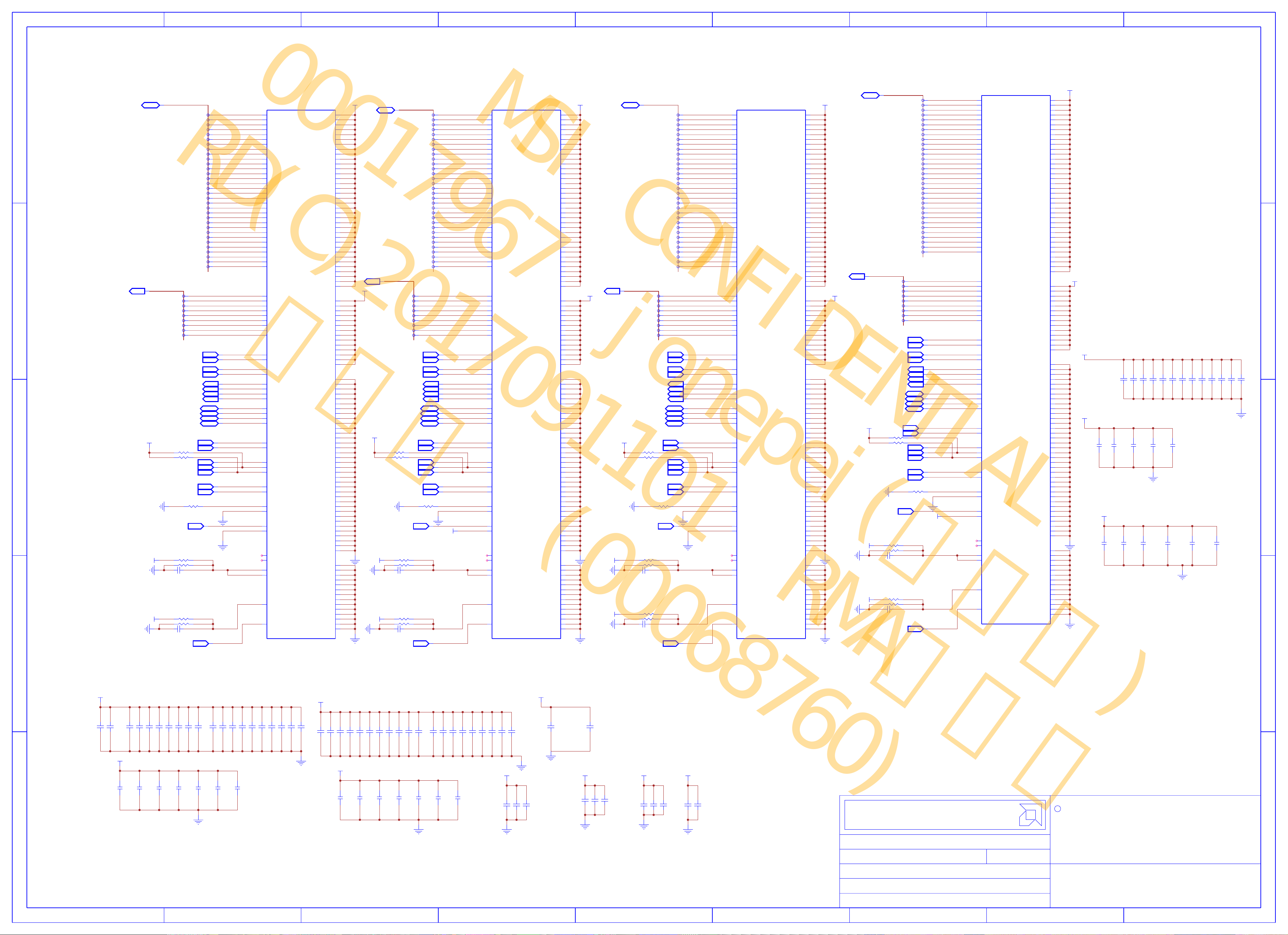
(4) GDDR5 Memory Channel A&B
(4) GDDR5 Memory Channel A&B
4 3
4 3
4 3
4 3
+MVDD
+MVDD
C2007
C2008
C2008
C2007
6.3V
6.3V
6.3V
6.3V
2 1
2 1
2 1
2 1
2 1
2 1
0.1uF
0.1uF
0.1uF
0.1uF
+MVDD
+MVDD
4.7uF4V4.7uF
4.7uF4V4.7uF
4V
4V
9
GDDR5
C2022
C2022
6.3V
6.3V
2 1
2 1
1uF
1uF
GDDR5
23CNOPN001
23CNOPN001
U2000
U2000
C2024
C2023
C2024
C2023
6.3V
6.3V
6.3V
6.3V
2 1
2 1
2 1
2 1
1uF
1uF
1uF
1uF
C2025
C2025
6.3V
6.3V
1uF
1uF
VDDQ_B1
VDDQ_B3
VDDQ_B12
VDDQ_B14
VDDQ_D1
VDDQ_D3
VDDQ_D12
VDDQ_D14
VDDQ_E5
VDDQ_E10
VDDQ_F1
VDDQ_F3
VDDQ_F12
VDDQ_F14
VDDQ_G2
VDDQ_G13
VDDQ_H3
VDDQ_H12
VDDQ_K3
VDDQ_K12
VDDQ_L2
VDDQ_L13
VDDQ_M1
VDDQ_M3
VDDQ_M12
VDDQ_M14
VDDQ_N5
VDDQ_N10
VDDQ_P1
VDDQ_P3
VDDQ_P12
VDDQ_P14
VDDQ_T1
VDDQ_T3
VDDQ_T12
VDDQ_T14
VDD_C5
VDD_C10
VDD_D11
VDD_G1
VDD_G4
VDD_G11
VDD_G14
VDD_L1
VDD_L4
VDD_L11
VDD_L14
VDD_P11
VDD_R5
VDD_R10
VSSQ_A1
VSSQ_A3
VSSQ_A12
VSSQ_A14
VSSQ_C1
VSSQ_C3
VSSQ_C4
VSSQ_C11
VSSQ_C12
VSSQ_C14
VSSQ_E1
VSSQ_E3
VSSQ_E12
VSSQ_E14
VSSQ_F5
VSSQ_F10
VSSQ_H2
VSSQ_H13
VSSQ_K2
VSSQ_K13
VSSQ_M5
VSSQ_M10
VSSQ_N1
VSSQ_N3
VSSQ_N12
VSSQ_N14
VSSQ_R1
VSSQ_R3
VSSQ_R4
VSSQ_R11
VSSQ_R12
VSSQ_R14
VSSQ_V1
VSSQ_V3
VSSQ_V12
VSSQ_V14
VSS_B5
VSS_B10
VSS_D10
VSS_G5
VSS_G10
VSS_H1
VSS_H14
VSS_K1
VSS_K14
VSS_L5
VSS_L10
VSS_P10
VSS_T5
VSS_T10
+MVDD
+MVDD
C2145
C2145
6.3V
6.3V
2 1
2 1
1uF
1uF
2 1
2 1
+MVDD
+MVDD
DQA0_<31..0>
BI
OUT
DQA0_<31..0>
MAA0_<8..0>
MAA0_<8..0>
4
4
DQA0_<30>
DQA0_<30>
3
3
30 17
30 17
4 3
4 3
4 3
4 3
4 3
4 3
4 3
4 3
4 3
4 3
4 3
4 3
4 3
4 3
4 3
4 3
4 3
4 3
4 3
4 3
4 3
4 3
4 3
4 3
4 3
4 3
4 3
4 3
4 3
4 3
4 3
4 3
4 3
4 3
4 3
4 3
4 3
4 3
4 3
4 3
4 3
4 3
4 3
4 3
4 3
4 3
4 3
4 3
4 3
4 3
4 3
4 3
4 3
4 3
4 3
4 3
4 3
4 3
4 3
4 3
4 3
4 3
4 3
4 3
8
8
4 3
4 3
7
7
4 3
4 3
6
6
4 3
4 3
5
5
4 3
4 3
4
4
4 3
4 3
3
3
4 3
4 3
2
2
4 3
4 3
1
1
4 3
4 3
0
0
DQA0_<31>
DQA0_<31>
31
31
DQA0_<29>
DQA0_<29>
29
29
DQA0_<28>
DQA0_<28>
28
28
DQA0_<27>
DQA0_<27>
27
27
DQA0_<24>
DQA0_<24>
24
24
DQA0_<26>
DQA0_<26>
26
26
DQA0_<25>
DQA0_<25>
25
25
DQA0_<17>
DQA0_<17>
17
17
DQA0_<16>
DQA0_<16>
16
16
DQA0_<18>
DQA0_<18>
18
18
DQA0_<21>
DQA0_<21>
21
21
DQA0_<19>
DQA0_<19>
19
19
DQA0_<23>
DQA0_<23>
23
23
DQA0_<20>
DQA0_<20>
20
20
DQA0_<22>
DQA0_<22>
22
22
DQA0_<2>
DQA0_<2>
2
2
DQA0_<3>
DQA0_<3>
3
3
DQA0_<1>
DQA0_<1>
1
1
DQA0_<4>
DQA0_<4>
4
4
DQA0_<0>
DQA0_<0>
0
0
DQA0_<6>
DQA0_<6>
6
6
DQA0_<7>
DQA0_<7>
7
7
DQA0_<5>
DQA0_<5>
5
5
DQA0_<15>
DQA0_<15>
15
15
DQA0_<13>
DQA0_<13>
13
13
DQA0_<14>
DQA0_<14>
14
14
DQA0_<12>
DQA0_<12>
12
12
DQA0_<11>
DQA0_<11>
11
11
DQA0_<8>
DQA0_<8>
8
8
DQA0_<10>
DQA0_<10>
10
10
DQA0_<9>
DQA0_<9>
9
9
MAA0_<8>
MAA0_<8>
MAA0_<7>
MAA0_<7>
MAA0_<6>
MAA0_<6>
MAA0_<5>
MAA0_<5>
MAA0_<4>
MAA0_<4>
MAA0_<3>
MAA0_<3>
MAA0_<2>
MAA0_<2>
MAA0_<1>
MAA0_<1>
MAA0_<0>
MAA0_<0>
M2
M2
DQ31__DQ7
M4
M4
DQ30__DQ6
N2
N2
DQ29__DQ5
N4
N4
DQ28__DQ4
T2
T2
DQ27__DQ3
T4
T4
DQ26__DQ2
V2
V2
DQ25__DQ1
V4
V4
DQ24__DQ0
M13
M13
DQ23__DQ15
M11
M11
DQ22__DQ14
N13
N13
DQ21__DQ13
N11
N11
DQ20__DQ12
T13
T13
DQ19__DQ11
T11
T11
DQ18__DQ10
V13
V13
DQ17__DQ9
V11
V11
DQ16__DQ8
F13
F13
DQ15__DQ23
F11
F11
DQ14__DQ22
E13
E13
DQ13__DQ21
E11
E11
DQ12__DQ20
B13
B13
DQ11__DQ19
B11
B11
DQ10__DQ18
A13
A13
DQ9__DQ17
A11
A11
DQ8__DQ16
F2
F2
DQ7__DQ31
F4
F4
DQ6__DQ30
E2
E2
DQ5__DQ29
E4
E4
DQ4__DQ28
B2
B2
DQ3__DQ27
B4
B4
DQ2__DQ26
A2
A2
DQ1__DQ25
A4
A4
DQ0__DQ24
J5
J5
RFU_A12_NC
K4
K4
A7_A8__A0_A10
K5
K5
A6_A11__A1_A9
K10
K10
A5_BA1__A3_BA3
K11
K11
A4_BA2__A2_BA0
H10
H10
A3_BA3__A5_BA1
H11
H11
A2_BA0__A4_BA2
H5
H5
A1_A9__A6_A11
H4
H4
A0_A10__A7_A8
C2018
C2018
6.3V
6.3V
2 1
2 1
1uF
1uF
C2131C2126C2122
C2131C2126C2122
R13
R13
C13
C13
P13
P13
D13
D13
J11
J11
J12
J12
G12
G12
L12
L12
J13
J13
J10
J10
A10
A10
V10
V10
J14
J14
C2019
C2019
6.3V
6.3V
2 1
2 1
1uF
1uF
D4
D4
WCK01__WCK23
D5
D5
WCK01#__WCK23#
P4
P4
WCK23__WCK01
P5
P5
WCK23#__WCK01#
R2
R2
EDC3__EDC0
EDC2__EDC1
EDC1__EDC2
C2
C2
EDC0__EDC3
P2
P2
DBI3#__DBI0#
DBI2#__DBI1#
DBI1#__DBI2#
D2
D2
DBI0#__DBI3#
G3
G3
RAS#__CAS#
L3
L3
CAS#__RAS#
J3
J3
CKE#
CK#
CK
CS#__WE#
WE#__CS#
ZQ
SEN
J2
J2
RESET#
J1
J1
MF
A5
A5
Vpp_NC
V5
V5
Vpp_NC1
VREFD1
VREFD2
VREFC
J4
J4
ABI#
C2020
C2021
C2021
C2020
6.3V
6.3V
6.3V
6.3V
2 1
2 1
2 1
2 1
1uF
1uF
1uF
1uF
+MVDD
+MVDD
+MVDD
+MVDD
C2010
C2010
6.3V
6.3V
2 1
2 1
0.1uF
0.1uF
+MVDD
+MVDD
R2003
R2003
R2004
R2004
R2098
R2098
C2003
C2003
R2297
R2297
R2296
R2296
C2296
C2296
C2000
C2011
C2001
C2001
C2011
C2000
6.3V
6.3V
6.3V
6.3V
6.3V
6.3V
2 1
2 1
2 1
2 1
2 1
2 1
0.1uF
0.1uF
0.1uF
0.1uF
0.1uF
0.1uF
4.7uF4V4.7uF4V4.7uF
4.7uF4V4.7uF4V4.7uF
4V
4V
3
3
4 3
4 3
R2099
R2099
1%
1%
C2012
C2012
6.3V
6.3V
2 1
2 1
0.1uF
0.1uF
60.4R
60.4R
1%
1%
60.4R
60.4R
1%
1%
2.37K
2.37K
1%
1%
5.49K
5.49K
21
21
1%
1%
1uF
1uF
6.3V
6.3V
2.37K
2.37K
1%
1%
5.49K
5.49K
21
21
1%
1%
1uF
1uF
6.3V
6.3V
3
3
C2013
C2013
6.3V
6.3V
2 1
2 1
0.1uF
0.1uF
C2127C2137C2136C2135
C2127C2137C2136C2135
3
3
3
3
3
3
3
3
3
3
3
3
3
3
3
3
3
3
3
3
21
21
21
21
3
3
3
3
3
3
3
3
R2002
120R
120R
1%
1%
IN
21
21
21
21
21
21
21
21
IN
C2014
C2014
6.3V
6.3V
0.1uF
0.1uF
2 1
2 1
3
3
3
3
3
3
3
3
IN
IN
IN
IN
IN
IN
IN
C2015
C2015
6.3V
6.3V
0.1uF
0.1uF
WCKA0_0
WCKA0_0
IN
WCKA0B_0
WCKA0B_0
IN
WCKA0_1
WCKA0_1
IN
WCKA0B_1
WCKA0B_1
IN
EDCA0_3
EDCA0_3
OUT
EDCA0_2
EDCA0_2
OUT
EDCA0_0
EDCA0_0
OUT
EDCA0_1
EDCA0_1
OUT
DDBIA0_3
DDBIA0_3
BI
DDBIA0_2
DDBIA0_2
BI
DDBIA0_0
DDBIA0_0
BI
DDBIA0_1
DDBIA0_1
BI
RASA0B
RASA0B
CASA0B
CASA0B
CLKA0B
CLKA0B
CLKA0
CLKA0
CKEA0
CKEA0
CSA0B_0
CSA0B_0
WEA0B
WEA0B
21
1% 1%
1% 1%
DRAM_RST
DRAM_RST
1%
1%
1%
1%
REFD_A0
REFD_A0
1%
1%
1%
1%
VREFC_U2000
VREFC_U2000
ADBIA0
ADBIA0
C2016
C2017
C2017
C2016
6.3V
6.3V
6.3V
6.3V
2 1
2 1
2 1
2 1
2 1
2 1
1uF
1uF
1uF
1uF
4.7uF4V4.7uF
4.7uF4V4.7uF
4V
4V
4 3
GDDR5
DQB0_<31..0>
+MVDD +MVDD +MVDD
+MVDD +MVDD +MVDD
4 3
B1
B1
B3
B3
B12
B12
B14
B14
D1
D1
D3
D3
D12
D12
D14
D14
E5
E5
E10
E10
F1
F1
F3
F3
F12
F12
F14
F14
G2
G2
G13
G13
H3
H3
H12
H12
K3
K3
K12
K12
L2
L2
L13
L13
M1
M1
M3
M3
M12
M12
M14
M14
N5
N5
N10
N10
P1
P1
P3
P3
P12
P12
P14
P14
T1
T1
T3
T3
T12
T12
T14
T14
C5
C5
C10
C10
D11
D11
G1
G1
G4
G4
G11
G11
G14
G14
L1
L1
L4
L4
L11
L11
L14
L14
P11
P11
R5
R5
R10
R10
A1
A1
A3
A3
A12
A12
A14
A14
C1
C1
C3
C3
C4
C4
C11
C11
C12
C12
C14
C14
E1
E1
E3
E3
E12
E12
E14
E14
F5
F5
F10
F10
H2
H2
H13
H13
K2
K2
K13
K13
M5
M5
M10
M10
N1
N1
N3
N3
N12
N12
N14
N14
R1
R1
R3
R3
R4
R4
R11
R11
R12
R12
R14
R14
V1
V1
V3
V3
V12
V12
V14
V14
B5
B5
B10
B10
D10
D10
G5
G5
G10
G10
H1
H1
H14
H14
K1
K1
K14
K14
L5
L5
L10
L10
P10
P10
T5
T5
T10
T10
C2100
C2100
6.3V
6.3V
2 1
2 1
1uF
1uF
4 3
3
3
OUT
4
4
+MVDD
+MVDD
+MVDD
+MVDD
+MVDD
+MVDD
+MVDD
+MVDD
C2101
C2102
C2103
C2103
C2102
C2101
6.3V
6.3V
6.3V
6.3V
6.3V
6.3V
2 1
2 1
2 1
2 1
2 1
2 1
1uF
1uF
1uF
1uF
1uF
1uF
4.7uF
4.7uF4V4.7uF4V4.7uF
4.7uF
4.7uF4V4.7uF4V4.7uF
4V
4V
4V
4V
C2104
C2104
6.3V
6.3V
2 1
2 1
1uF
1uF
BI
MAA1_<8..0>
MAA1_<8..0>
R2203
R2203
R2204
R2204
3
3
R2299
R2299
R2298
R2298
C2298
C2298
R2209
R2209
R2210
R2210
C2241
C2241
C2106
C2105
C2105
C2106
6.3V
6.3V
6.3V
6.3V
2 1
2 1
1uF
1uF
1uF
1uF
C2238C2237C2236
C2238C2237C2236
DQA1_<31..0>
DQA1_<31..0>
8
8
0
0
1
1
3
3
2
2
5
5
4
4
6
6
7
7
3
3
3
3
3
3
3
3
3
3
3
3
3
3
3
3
3
3
3
3
3
3
3
3
3
3
3
3
21
21
60.4R
60.4R
21
21
1%
1%
60.4R
60.4R
1%
1%
3
3
3
3
3
3
3
3
4 3
4 3
IN
21
21
2.37K
2.37K
21
21
1%
1%
5.49K
5.49K
21
21
1%
1%
1uF
1uF
6.3V
6.3V
1%
1%
21
21
2.37K
2.37K
21
21
1%
1%
5.49K
5.49K
21
21
1%
1%
1uF
1uF
6.3V
6.3V
3
3
IN
C2107
C2108
C2108
C2107
6.3V
6.3V
6.3V
6.3V
2 1
2 1
2 1
2 1
2 1
2 1
1uF
1uF
1uF
1uF
4
4
3
DQA1_<17>
DQA1_<17>
3
4 3
4 3
4 3
4 3
4 3
4 3
4 3
4 3
4 3
4 3
4 3
4 3
4 3
4 3
4 3
4 3
4 3
4 3
4 3
4 3
4 3
4 3
4 3
4 3
4 3
4 3
4 3
4 3
4 3
4 3
4 3
4 3
4 3
4 3
4 3
4 3
4 3
4 3
4 3
4 3
4 3
4 3
4 3
4 3
4 3
4 3
4 3
4 3
4 3
4 3
4 3
4 3
4 3
4 3
4 3
4 3
4 3
4 3
4 3
4 3
4 3
4 3
IN
IN
IN
IN
OUT
OUT
OUT
OUT
BI
BI
BI
BI
IN
IN
IN
IN
IN
IN
IN
1%
1%
1%
1%
1%
1%
1%
1%
C2109
C2109
6.3V
6.3V
1uF
1uF
4.7uF4V4.7uF
4.7uF4V4.7uF
4V
4V
DQA1_<23>
DQA1_<23>
23 25
23 25
DQA1_<16>
DQA1_<16>
16
16
DQA1_<20>
DQA1_<20>
20
20
DQA1_<19>
DQA1_<19>
19
19
DQA1_<22>
DQA1_<22>
22
22
DQA1_<18>
DQA1_<18>
18
18
DQA1_<21>
DQA1_<21>
21
21
DQA1_<30>
DQA1_<30>
30
30
DQA1_<24>
DQA1_<24>
24
24
DQA1_<29>
DQA1_<29>
29
29
DQA1_<27>
DQA1_<27>
27
27
DQA1_<28>
DQA1_<28>
28
28
DQA1_<25>
DQA1_<25>
25
25
DQA1_<31>
DQA1_<31>
31
31
DQA1_<26>
DQA1_<26>
26
26
DQA1_<14>
DQA1_<14>
14
14
DQA1_<15>
DQA1_<15>
15
15
DQA1_<12>
DQA1_<12>
12
12
DQA1_<8>
DQA1_<8>
8
8
DQA1_<13>
DQA1_<13>
13
13
DQA1_<9>
DQA1_<9>
9
9
DQA1_<11>
DQA1_<11>
11
11
DQA1_<10>
DQA1_<10>
10
10
DQA1_<1>
DQA1_<1>
1
1
DQA1_<0>
DQA1_<0>
0
0
DQA1_<6>
DQA1_<6>
6
6
DQA1_<5>
DQA1_<5>
5
5
DQA1_<2>
DQA1_<2>
2
2
DQA1_<4>
DQA1_<4>
4
4
DQA1_<3>
DQA1_<3>
3
3
DQA1_<7>
DQA1_<7>
7
7
4 3
4 3
MAA1_<8>
MAA1_<8>
4 3
4 3
MAA1_<0>
MAA1_<0>
4 3
4 3
MAA1_<1>
MAA1_<1>
4 3
4 3
MAA1_<3>
MAA1_<3>
4 3
4 3
MAA1_<2>
MAA1_<2>
MAA1_<5>
MAA1_<5>
4 3
4 3
4 3
4 3
MAA1_<4>
MAA1_<4>
MAA1_<6>
MAA1_<6>
4 3
4 3
4 3
4 3
MAA1_<7>
MAA1_<7>
WCKA1_0
WCKA1_0
WCKA1B_0
WCKA1B_0
WCKA1_1
WCKA1_1
WCKA1B_1
WCKA1B_1
EDCA1_2
EDCA1_2
EDCA1_3
EDCA1_3
EDCA1_1
EDCA1_1
EDCA1_0
EDCA1_0
DDBIA1_2
DDBIA1_2
DDBIA1_3
DDBIA1_3
DDBIA1_1
DDBIA1_1
DDBIA1_0
DDBIA1_0
CASA1B
CASA1B
RASA1B
RASA1B
CLKA1B
CLKA1B
CLKA1
CLKA1
CKEA1
CKEA1
WEA1B
WEA1B
CSA1B_0
CSA1B_0
R2201
R2201R2002
2121
21
120R
120R
1%
1%
DRAM_RST
DRAM_RST
+MVDD
+MVDD
REFD_A1
REFD_A1
VREFC_U2200
VREFC_U2200
ADBIA1
ADBIA1
C2110
C2111
C2112
C2112
C2111
C2110
6.3V
6.3V
6.3V
6.3V
6.3V
1uF
1uF
6.3V
2 1
2 1
2 1
2 1
1uF
1uF
1uF
1uF
2 1
2 1
C2113
C2113
6.3V
6.3V
2 1
2 1
1uF
1uF
C2234C2228C2235C2227
C2234C2228C2235C2227
4.7uF
4.7uF
4V
4V
2 1
2 1
M2
M2
M4
M4
N2
N2
N4
N4
T2
T2
T4
T4
V2
V2
V4
V4
M13
M13
M11
M11
N13
N13
N11
N11
T13
T13
T11
T11
V13
V13
V11
V11
F13
F13
F11
F11
E13
E13
E11
E11
B13
B13
B11
B11
A13
A13
A11
A11
F2
F2
F4
F4
E2
E2
E4
E4
B2
B2
B4
B4
A2
A2
A4
A4
J5
J5
K4
K4
K5
K5
K10
K10
K11
K11
H10
H10
H11
H11
H5
H5
H4
H4
D4
D4
D5
D5
P4
P4
P5
P5
R2
R2
R13
R13
C13
C13
C2
C2
P2
P2
P13
P13
D13
D13
D2
D2
G3
G3
L3
L3
J3
J3
J11
J11
J12
J12
G12
G12
L12
L12
J13
J13
J10
J10
J2
J2
J1
J1
A5
A5
V5
V5
A10
A10
V10
V10
J14
J14
J4
J4
C2114
C2114
6.3V
6.3V
2 1
2 1
1uF
1uF
C2115
C2115
6.3V
6.3V
2 1
2 1
1uF
1uF
DQ31__DQ7
DQ30__DQ6
DQ29__DQ5
DQ28__DQ4
DQ27__DQ3
DQ26__DQ2
DQ25__DQ1
DQ24__DQ0
DQ23__DQ15
DQ22__DQ14
DQ21__DQ13
DQ20__DQ12
DQ19__DQ11
DQ18__DQ10
DQ17__DQ9
DQ16__DQ8
DQ15__DQ23
DQ14__DQ22
DQ13__DQ21
DQ12__DQ20
DQ11__DQ19
DQ10__DQ18
DQ9__DQ17
DQ8__DQ16
DQ7__DQ31
DQ6__DQ30
DQ5__DQ29
DQ4__DQ28
DQ3__DQ27
DQ2__DQ26
DQ1__DQ25
DQ0__DQ24
RFU_A12_NC
A7_A8__A0_A10
A6_A11__A1_A9
A5_BA1__A3_BA3
A4_BA2__A2_BA0
A3_BA3__A5_BA1
A2_BA0__A4_BA2
A1_A9__A6_A11
A0_A10__A7_A8
WCK01__WCK23
WCK01#__WCK23#
WCK23__WCK01
WCK23#__WCK01#
EDC3__EDC0
EDC2__EDC1
EDC1__EDC2
EDC0__EDC3
DBI3#__DBI0#
DBI2#__DBI1#
DBI1#__DBI2#
DBI0#__DBI3#
RAS#__CAS#
CAS#__RAS#
CKE#
CK#
CK
CS#__WE#
WE#__CS#
ZQ
SEN
RESET#
MF
Vpp_NC
Vpp_NC1
VREFD1
VREFD2
VREFC
ABI#
23CNOPN001
23CNOPN001
U2200
U2200
VDDQ_B1
VDDQ_B3
VDDQ_B12
VDDQ_B14
VDDQ_D1
VDDQ_D3
VDDQ_D12
VDDQ_D14
VDDQ_E5
VDDQ_E10
VDDQ_F1
VDDQ_F3
VDDQ_F12
VDDQ_F14
VDDQ_G2
VDDQ_G13
VDDQ_H3
VDDQ_H12
VDDQ_K3
VDDQ_K12
VDDQ_L2
VDDQ_L13
VDDQ_M1
VDDQ_M3
VDDQ_M12
VDDQ_M14
VDDQ_N5
VDDQ_N10
VDDQ_P1
VDDQ_P3
VDDQ_P12
VDDQ_P14
VDDQ_T1
VDDQ_T3
VDDQ_T12
VDDQ_T14
VDD_C5
VDD_C10
VDD_D11
VDD_G1
VDD_G4
VDD_G11
VDD_G14
VDD_L1
VDD_L4
VDD_L11
VDD_L14
VDD_P11
VDD_R5
VDD_R10
VSSQ_A1
VSSQ_A3
VSSQ_A12
VSSQ_A14
VSSQ_C1
VSSQ_C3
VSSQ_C4
VSSQ_C11
VSSQ_C12
VSSQ_C14
VSSQ_E1
VSSQ_E3
VSSQ_E12
VSSQ_E14
VSSQ_F5
VSSQ_F10
VSSQ_H2
VSSQ_H13
VSSQ_K2
VSSQ_K13
VSSQ_M5
VSSQ_M10
VSSQ_N1
VSSQ_N3
VSSQ_N12
VSSQ_N14
VSSQ_R1
VSSQ_R3
VSSQ_R4
VSSQ_R11
VSSQ_R12
VSSQ_R14
VSSQ_V1
VSSQ_V3
VSSQ_V12
VSSQ_V14
VSS_B5
VSS_B10
VSS_D10
VSS_G5
VSS_G10
VSS_H1
VSS_H14
VSS_K1
VSS_K14
VSS_L5
VSS_L10
VSS_P10
VSS_T5
VSS_T10
+MVDD
+MVDD
C2116
C2117
C2118
C2118
C2117
C2116
6.3V
6.3V
6.3V
6.3V
6.3V
6.3V
2 1
2 1
2 1
2 1
1uF
1uF
1uF
1uF
1uF
1uF
+MVDD +MVDD +MVDD
+MVDD +MVDD +MVDD
C2124
C2125
C2130
C2130
C2125
C2124
6.3V
6.3V
6.3V
6.3V
6.3V
6.3V
2 1
2 1
2 1
2 1
2 1
2 1
10uF
10uF
10uF
10uF
10uF
10uF
2 1
2 1
C2201
C2201
6.3V
6.3V
1uF
1uF
B1
B1
B3
B3
B12
B12
B14
B14
D1
D1
D3
D3
D12
D12
D14
D14
E5
E5
E10
E10
F1
F1
F3
F3
F12
F12
F14
F14
G2
G2
G13
G13
H3
H3
H12
H12
K3
K3
K12
K12
L2
L2
L13
L13
M1
M1
M3
M3
M12
M12
M14
M14
N5
N5
N10
N10
P1
P1
P3
P3
P12
P12
P14
P14
T1
T1
T3
T3
T12
T12
T14
T14
+MVDD +MVDD
+MVDD +MVDD
C5
C5
C10
C10
D11
D11
G1
G1
G4
G4
G11
G11
G14
G14
L1
L1
L4
L4
L11
L11
L14
L14
P11
P11
R5
R5
R10
R10
A1
A1
A3
A3
A12
A12
A14
A14
C1
C1
C3
C3
C4
C4
C11
C11
C12
C12
C14
C14
E1
E1
E3
E3
E12
E12
E14
E14
F5
F5
F10
F10
H2
H2
H13
H13
K2
K2
K13
K13
M5
M5
M10
M10
N1
N1
N3
N3
N12
N12
N14
N14
R1
R1
R3
R3
R4
R4
R11
R11
R12
R12
R14
R14
V1
V1
V3
V3
V12
V12
V14
V14
B5
B5
B10
B10
D10
D10
G5
G5
G10
G10
H1
H1
H14
H14
K1
K1
K14
K14
L5
L5
L10
L10
P10
P10
T5
T5
T10
T10
2 1
2 1
4 3
4 3
C2205
C2205
6.3V
6.3V
2 1
2 1
1uF
1uF
C2337
C2337
6.3V
6.3V
2 1
2 1
10uF
10uF
+MVDD
+MVDD
+MVDD
+MVDD
C2338
C2338
6.3V
6.3V
2 1
2 1
10uF
10uF
4 3
4 3
OUT
C2339
C2339
6.3V
6.3V
10uF
10uF
+MVDD
+MVDD
7
DQB0_<31..0>
BI
MAB0_<8..0>
MAB0_<8..0>
R2403
R2403
R2404
R2404
3
3
R2499
R2499
R2498
R2498
C2498
C2498
1%
1%
R2497
R2497
R2496
R2496
C2496
C2496
2 1
2 1
60.4R
60.4R
1%
1%
60.4R
60.4R
1%
1%
4 3
4 3
2.37K
2.37K
1%
1%
5.49K
5.49K
21
21
1%
1%
1uF
1uF
6.3V
6.3V
2.37K
2.37K
1%
1%
5.49K
5.49K
21
21
1%
1%
1uF
1uF
6.3V
6.3V
C2030
C2030
6.3V
6.3V
10uF
10uF
2 1
2 1
3
3
3
3
3
3
3
3
3
3
3
3
3
3
3
3
3
3
3
3
21
21
21
21
3
3
3
3
3
3
3
3
IN
21
21
21
21
21
21
21
21
3
3
C2031
C2031
6.3V
6.3V
10uF
10uF
4 3
4 3
4 3
4 3
4 3
4 3
4 3
4 3
4 3
4 3
4 3
4 3
4 3
4 3
4 3
4 3
4 3
4 3
4 3
4 3
4 3
4 3
4 3
4 3
4 3
4 3
4 3
4 3
4 3
4 3
4 3
4 3
4 3
4 3
4 3
4 3
4 3
4 3
4 3
4 3
4 3
4 3
4 3
4 3
4 3
4 3
4 3
4 3
4 3
4 3
4 3
4 3
4 3
4 3
4 3
4 3
4 3
4 3
4 3
4 3
4 3
4 3
8
8
7
7
6
6
5
5
4
4
3
3
2
2
1
1
0
0
3
3
3
3
3
3
3
3
IN
IN
R2400
R2400
120R
120R
1%
1%
1%
1%
1%
1%
1%
1%
1%
1%
IN
C2032
C2032
6.3V
6.3V
2 1
2 1
10uF
10uF
4
4
3
3
DQB0_<24>
DQB0_<24>
24
24
DQB0_<25>
DQB0_<25>
DQB0_<31>
DQB0_<31>
31
31
DQB0_<30>
DQB0_<30>
30
30
DQB0_<29>
DQB0_<29>
29
29
DQB0_<26>
DQB0_<26>
26
26
DQB0_<28>
DQB0_<28>
28
28
DQB0_<27>
DQB0_<27>
27
27
DQB0_<16>
DQB0_<16>
16
16
DQB0_<17>
DQB0_<17>
17
17
DQB0_<18>
DQB0_<18>
18
18
DQB0_<23>
DQB0_<23>
23
23
DQB0_<20>
DQB0_<20>
20
20
DQB0_<21>
DQB0_<21>
21
21
DQB0_<19>
DQB0_<19>
19
19
DQB0_<22>
DQB0_<22>
22
22
DQB0_<5>
DQB0_<5>
5
5
DQB0_<4>
DQB0_<4>
4
4
DQB0_<2>
DQB0_<2>
2
2
DQB0_<3>
DQB0_<3>
3
3
DQB0_<1>
DQB0_<1>
1
1
DQB0_<7>
DQB0_<7>
7
7
DQB0_<0>
DQB0_<0>
0
0
DQB0_<6>
DQB0_<6>
6
6
DQB0_<13>
DQB0_<13>
13
13
DQB0_<15>
DQB0_<15>
15
15
DQB0_<14>
DQB0_<14>
14
14
DQB0_<12>
DQB0_<12>
12
12
DQB0_<10>
DQB0_<10>
10
10
DQB0_<11>
DQB0_<11>
11
11
DQB0_<8>
DQB0_<8>
8
8
DQB0_<9>
DQB0_<9>
9
9
4 3
4 3
MAB0_<8>
MAB0_<8>
MAB0_<7>
MAB0_<7>
4 3
4 3
MAB0_<6>
MAB0_<6>
4 3
4 3
MAB0_<5>
MAB0_<5>
4 3
4 3
MAB0_<4>
MAB0_<4>
4 3
4 3
MAB0_<3>
MAB0_<3>
4 3
4 3
MAB0_<2>
MAB0_<2>
4 3
4 3
MAB0_<1>
MAB0_<1>
4 3
4 3
MAB0_<0>
MAB0_<0>
4 3
4 3
WCKB0_0
IN
IN
IN
IN
OUT
OUT
OUT
OUT
BI
BI
BI
BI
IN
IN
IN
IN
IN
WCKB0_0
WCKB0B_0
WCKB0B_0
WCKB0_1
WCKB0_1
WCKB0B_1
WCKB0B_1
EDCB0_3
EDCB0_3
EDCB0_2
EDCB0_2
EDCB0_0
EDCB0_0
EDCB0_1
EDCB0_1
DDBIB0_3
DDBIB0_3
DDBIB0_2
DDBIB0_2
DDBIB0_0
DDBIB0_0
DDBIB0_1
DDBIB0_1
RASB0B
RASB0B
CASB0B
CASB0B
CLKB0B
CLKB0B
CLKB0
CLKB0
CKEB0
CKEB0
CSB0B_0
CSB0B_0
WEB0B
WEB0B
21 J13
21
1%
1%
DRAM_RST
DRAM_RST
REFD_B0
REFD_B0
VREFC_U2400
VREFC_U2400
ADBIB0
ADBIB0
+MVDD
+MVDD
C2233
C2230
C2230
C2233
6.3V
6.3V
6.3V
6.3V
2 1
2 1
2 1
2 1
10uF
10uF
10uF
10uF
M2
M2
DQ31__DQ7
M4
M4
DQ30__DQ6
N2
N2
DQ29__DQ5
N4
N4
DQ28__DQ4
T2
T2
DQ27__DQ3
T4
T4
DQ26__DQ2
V2
V2
DQ25__DQ1
V4
V4
DQ24__DQ0
M13
M13
DQ23__DQ15
M11
M11
DQ22__DQ14
N13
N13
DQ21__DQ13
N11
N11
DQ20__DQ12
T13
T13
DQ19__DQ11
T11
T11
DQ18__DQ10
V13
V13
DQ17__DQ9
V11
V11
DQ16__DQ8
F13
F13
DQ15__DQ23
F11
F11
DQ14__DQ22
E13
E13
DQ13__DQ21
E11
E11
DQ12__DQ20
B13
B13
DQ11__DQ19
B11
B11
DQ10__DQ18
A13
A13
DQ9__DQ17
A11
A11
DQ8__DQ16
F2
F2
DQ7__DQ31
F4
F4
DQ6__DQ30
E2
E2
DQ5__DQ29
E4
E4
DQ4__DQ28
B2
B2
DQ3__DQ27
B4
B4
DQ2__DQ26
A2
A2
DQ1__DQ25
A4
A4
DQ0__DQ24
J5
J5
RFU_A12_NC
K4
K4
A7_A8__A0_A10
K5
K5
A6_A11__A1_A9
K10
K10
A5_BA1__A3_BA3
K11
K11
A4_BA2__A2_BA0
H10
H10
A3_BA3__A5_BA1
H11
H11
A2_BA0__A4_BA2
H5
H5
A1_A9__A6_A11
H4
H4
A0_A10__A7_A8
D4
D4
WCK01__WCK23
D5
D5
WCK01#__WCK23#
P4
P4
WCK23__WCK01
P5
P5
WCK23#__WCK01#
R2
R2
EDC3__EDC0
R13
R13
EDC2__EDC1
C13
C13
EDC1__EDC2
C2
C2
EDC0__EDC3
P2
P2
DBI3#__DBI0#
P13
P13
DBI2#__DBI1#
D13
D13
DBI1#__DBI2#
D2
D2
DBI0#__DBI3#
G3
G3
RAS#__CAS#
L3
L3
CAS#__RAS#
J3
J3
CKE#
J11
J11
CK#
J12
J12
CK
G12
G12
CS#__WE#
L12
L12
WE#__CS#
J13
ZQ
J10
J10
SEN
J2
J2
RESET#
J1
J1
MF
A5
A5
Vpp_NC
V5
V5
Vpp_NC1
A10
A10
VREFD1
V10
V10
VREFD2
J14
J14
VREFC
J4
J4
ABI#
58 6 3
GDDR5
23CNOPN001
23CNOPN001
U2400
U2400
VDDQ_B12
VDDQ_B14
VDDQ_D12
VDDQ_D14
VDDQ_E10
VDDQ_F12
VDDQ_F14
VDDQ_G13
VDDQ_H12
VDDQ_K12
VDDQ_L13
VDDQ_M12
VDDQ_M14
VDDQ_N10
VDDQ_P12
VDDQ_P14
VDDQ_T12
VDDQ_T14
VSSQ_A12
VSSQ_A14
VSSQ_C11
VSSQ_C12
VSSQ_C14
VSSQ_E12
VSSQ_E14
VSSQ_F10
VSSQ_H13
VSSQ_K13
VSSQ_M10
VSSQ_N12
VSSQ_N14
VSSQ_R11
VSSQ_R12
VSSQ_R14
VSSQ_V12
VSSQ_V14
4
VDDQ_B1
VDDQ_B3
VDDQ_D1
VDDQ_D3
VDDQ_E5
VDDQ_F1
VDDQ_F3
VDDQ_G2
VDDQ_H3
VDDQ_K3
VDDQ_L2
VDDQ_M1
VDDQ_M3
VDDQ_N5
VDDQ_P1
VDDQ_P3
VDDQ_T1
VDDQ_T3
VDD_C5
VDD_C10
VDD_D11
VDD_G1
VDD_G4
VDD_G11
VDD_G14
VDD_L1
VDD_L4
VDD_L11
VDD_L14
VDD_P11
VDD_R5
VDD_R10
VSSQ_A1
VSSQ_A3
VSSQ_C1
VSSQ_C3
VSSQ_C4
VSSQ_E1
VSSQ_E3
VSSQ_F5
VSSQ_H2
VSSQ_K2
VSSQ_M5
VSSQ_N1
VSSQ_N3
VSSQ_R1
VSSQ_R3
VSSQ_R4
VSSQ_V1
VSSQ_V3
VSS_B5
VSS_B10
VSS_D10
VSS_G5
VSS_G10
VSS_H1
VSS_H14
VSS_K1
VSS_K14
VSS_L5
VSS_L10
VSS_P10
VSS_T5
VSS_T10
B1
B1
B3
B3
B12
B12
B14
B14
D1
D1
D3
D3
D12
D12
D14
D14
E5
E5
E10
E10
F1
F1
F3
F3
F12
F12
F14
F14
G2
G2
G13
G13
H3
H3
H12
H12
K3
K3
K12
K12
L2
L2
L13
L13
M1
M1
M3
M3
M12
M12
M14
M14
N5
N5
N10
N10
P1
P1
P3
P3
P12
P12
P14
P14
T1
T1
T3
T3
T12
T12
T14
T14
C5
C5
C10
C10
D11
D11
G1
G1
G4
G4
G11
G11
G14
G14
L1
L1
L4
L4
L11
L11
L14
L14
P11
P11
R5
R5
R10
R10
A1
A1
A3
A3
A12
A12
A14
A14
C1
C1
C3
C3
C4
C4
C11
C11
C12
C12
C14
C14
E1
E1
E3
E3
E12
E12
E14
E14
F5
F5
F10
F10
H2
H2
H13
H13
K2
K2
K13
K13
M5
M5
M10
M10
N1
N1
N3
N3
N12
N12
N14
N14
R1
R1
R3
R3
R4
R4
R11
R11
R12
R12
R14
R14
V1
V1
V3
V3
V12
V12
V14
V14
B5
B5
B10
B10
D10
D10
G5
G5
G10
G10
H1
H1
H14
H14
K1
K1
K14
K14
L5
L5
L10
L10
P10
P10
T5
T5
T10
T10
4 3
4 3
4 3
OUT
+MVDD
+MVDD
+MVDD
+MVDD
AMD - PLATFORM HARDWARE ENG
AMD - PLATFORM HARDWARE ENG
#48, No.1387, ZHANGDONG ROAD
#48, No.1387, ZHANGDONG ROAD
SHANGHAI, CHINA 201203
SHANGHAI, CHINA 201203
SHEET:
DATE:
SHEET NUMBER:
DOCUMENT NUMBER:
NOTES:
DQB1_<31..0>
DQB1_<31..0>
BI
MAB1_<8..0>
MAB1_<8..0>
3
3
3
3
3
3
3
3
3
3
3
3
3
3
3
3
3
3
3
3
3
3
3
3
+MVDD
+MVDD
R2603
R2603
R2604
R2604
R2699
R2699
R2698
R2698
C2698
C2698
R2697
R2697
R2696
R2696
C2696
C2696
GDDR5 CHA&B
GDDR5 CHA&B
NOTE
NOTE
3
3
3
3
60.4R
60.4R
1%
1%
60.4R
60.4R
3
3
1%
1%
3
3
3
3
3
3
3
3
4 3
4 3
IN
21
21
2.37K
2.37K
21
21
1%
1%
5.49K
5.49K
21
21
1%
1%
1uF
1uF
6.3V
6.3V
21
21
2.37K
2.37K
21
21
1%
1%
5.49K
5.49K
21
21
1%
1%
1uF
1uF
6.3V
6.3V
3
3
Fri Oct 28 17:09:35 2016
Fri Oct 28 17:09:35 2016
18
18
4 3
4 3
20
20
4 3
4 3
16
16
4 3
4 3
19
19
4 3
4 3
17
17
4 3
4 3
22
22
4 3
4 3
21
21
4 3
4 3
23
23
4 3
4 3
30
30
4 3
4 3
27
27
4 3
4 3
29
29
4 3
4 3
25
25
4 3
4 3
26
26
4 3
4 3
24
24
4 3
4 3
28
28
4 3
4 3
31
31
4 3
4 3
14
14
4 3
4 3
15
15
4 3
4 3
13
13
4 3
4 3
8
8
4 3
4 3
11
11
4 3
4 3
9
9
4 3
4 3
12
12
4 3
4 3
10
10
4 3
4 3
3
3
4 3
4 3
0
0
4 3
4 3
2
2
4 3
4 3
1
1
4 3
4 3
5
5
4 3
4 3
6
6
4 3
4 3
4
4
4 3
4 3
7
7
4 3
4 3
8
8
4 3
4 3
0
0
4 3
4 3
1
1
4 3
4 3
3
3
4 3
4 3
2
2
4 3
4 3
5
5
4 3
4 3
4
4
4 3
4 3
6
6
4 3
4 3
7
7
IN
IN
IN
IN
OUT
OUT
OUT
OUT
BI
BI
BI
BI
IN
IN
21
21
21
IN
IN
IN
IN
IN
R2601
R2601
120R
120R
1%
1%
+MVDD
+MVDD
1%
1%
1%
1%
1%
1%
1%
1%
VREFC_U2600
VREFC_U2600
IN
105_CXXX00_00A
105_CXXX00_00A
4
4
3
DQB1_<18>
DQB1_<18>
3
DQB1_<20>
DQB1_<20>
DQB1_<16>
DQB1_<16>
DQB1_<19>
DQB1_<19>
DQB1_<17>
DQB1_<17>
DQB1_<22>
DQB1_<22>
DQB1_<21>
DQB1_<21>
DQB1_<23>
DQB1_<23>
DQB1_<30>
DQB1_<30>
DQB1_<27>
DQB1_<27>
DQB1_<29>
DQB1_<29>
DQB1_<25>
DQB1_<25>
DQB1_<26>
DQB1_<26>
DQB1_<24>
DQB1_<24>
DQB1_<28>
DQB1_<28>
DQB1_<31>
DQB1_<31>
DQB1_<14>
DQB1_<14>
DQB1_<15>
DQB1_<15>
DQB1_<13>
DQB1_<13>
DQB1_<8>
DQB1_<8>
DQB1_<11>
DQB1_<11>
DQB1_<9>
DQB1_<9>
DQB1_<12>
DQB1_<12>
DQB1_<10>
DQB1_<10>
DQB1_<3>
DQB1_<3>
DQB1_<0>
DQB1_<0>
DQB1_<2>
DQB1_<2>
DQB1_<1>
DQB1_<1>
DQB1_<5>
DQB1_<5>
DQB1_<6>
DQB1_<6>
DQB1_<4>
DQB1_<4>
DQB1_<7>
DQB1_<7>
MAB1_<8>
MAB1_<8>
MAB1_<0>
MAB1_<0>
MAB1_<1>
MAB1_<1>
MAB1_<3>
MAB1_<3>
MAB1_<2>
MAB1_<2>
MAB1_<5>
MAB1_<5>
MAB1_<4>
MAB1_<4>
MAB1_<6>
MAB1_<6>
MAB1_<7>
MAB1_<7>
WCKB1_0
WCKB1_0
WCKB1B_0
WCKB1B_0
WCKB1_1
WCKB1_1
WCKB1B_1
WCKB1B_1
EDCB1_2
EDCB1_2
EDCB1_3
EDCB1_3
EDCB1_1
EDCB1_1
EDCB1_0
EDCB1_0
DDBIB1_2
DDBIB1_2
DDBIB1_3
DDBIB1_3
DDBIB1_1
DDBIB1_1
DDBIB1_0
DDBIB1_0
CASB1B
CASB1B
RASB1B
RASB1B
CLKB1B
CLKB1B
CLKB1
CLKB1
CKEB1
CKEB1
WEB1B
WEB1B
CSB1B_0
CSB1B_0
21 J13
21
1%
1%
DRAM_RST
DRAM_RST
REFD_B1
REFD_B1
ADBIB1
ADBIB1
OF
M13
M13
M11
M11
N13
N13
N11
N11
T13
T13
T11
T11
V13
V13
V11
V11
F13
F13
F11
F11
E13
E13
E11
E11
B13
B13
B11
B11
A13
A13
A11
A11
K10
K10
K11
K11
H10
H10
H11
H11
R13
R13
C13
C13
P13
P13
D13
D13
J11
J11
J12
J12
G12
G12
L12
L12
J13
J10
J10
A10
A10
V10
V10
J14
J14
214
214
M2
M2
DQ31__DQ7
M4
M4
DQ30__DQ6
N2
N2
DQ29__DQ5
N4
N4
DQ28__DQ4
T2
T2
DQ27__DQ3
T4
T4
DQ26__DQ2
V2
V2
DQ25__DQ1
V4
V4
DQ24__DQ0
DQ23__DQ15
DQ22__DQ14
DQ21__DQ13
DQ20__DQ12
DQ19__DQ11
DQ18__DQ10
DQ17__DQ9
DQ16__DQ8
DQ15__DQ23
DQ14__DQ22
DQ13__DQ21
DQ12__DQ20
DQ11__DQ19
DQ10__DQ18
DQ9__DQ17
DQ8__DQ16
F2
F2
DQ7__DQ31
F4
F4
DQ6__DQ30
E2
E2
DQ5__DQ29
E4
E4
DQ4__DQ28
B2
B2
DQ3__DQ27
B4
B4
DQ2__DQ26
A2
A2
DQ1__DQ25
A4
A4
DQ0__DQ24
J5
J5
RFU_A12_NC
K4
K4
A7_A8__A0_A10
K5
K5
A6_A11__A1_A9
A5_BA1__A3_BA3
A4_BA2__A2_BA0
A3_BA3__A5_BA1
A2_BA0__A4_BA2
H5
H5
A1_A9__A6_A11
H4
H4
A0_A10__A7_A8
D4
D4
WCK01__WCK23
D5
D5
WCK01#__WCK23#
P4
P4
WCK23__WCK01
P5
P5
WCK23#__WCK01#
R2
R2
EDC3__EDC0
EDC2__EDC1
EDC1__EDC2
C2
C2
EDC0__EDC3
P2
P2
DBI3#__DBI0#
DBI2#__DBI1#
DBI1#__DBI2#
D2
D2
DBI0#__DBI3#
G3
G3
RAS#__CAS#
L3
L3
CAS#__RAS#
J3
J3
CKE#
CK#
CK
CS#__WE#
WE#__CS#
ZQ
SEN
J2
J2
RESET#
J1
J1
MF
A5
A5
Vpp_NC
V5
V5
Vpp_NC1
VREFD1
VREFD2
VREFC
J4
J4
ABI#
REV:
GDDR5
GDDR5
23CNOPN001
23CNOPN001
U2600
U2600
1.0
1.0
+MVDD
+MVDD
B1
VDDQ_B1
VDDQ_B3
VDDQ_B12
VDDQ_B14
VDDQ_D1
VDDQ_D3
VDDQ_D12
VDDQ_D14
VDDQ_E5
VDDQ_E10
VDDQ_F1
VDDQ_F3
VDDQ_F12
VDDQ_F14
VDDQ_G2
VDDQ_G13
VDDQ_H3
VDDQ_H12
VDDQ_K3
VDDQ_K12
VDDQ_L2
VDDQ_L13
VDDQ_M1
VDDQ_M3
VDDQ_M12
VDDQ_M14
VDDQ_N5
VDDQ_N10
VDDQ_P1
VDDQ_P3
VDDQ_P12
VDDQ_P14
VDDQ_T1
VDDQ_T3
VDDQ_T12
VDDQ_T14
VDD_C5
VDD_C10
VDD_D11
VDD_G1
VDD_G4
VDD_G11
VDD_G14
VDD_L1
VDD_L4
VDD_L11
VDD_L14
VDD_P11
VDD_R5
VDD_R10
VSSQ_A1
VSSQ_A3
VSSQ_A12
VSSQ_A14
VSSQ_C1
VSSQ_C3
VSSQ_C4
VSSQ_C11
VSSQ_C12
VSSQ_C14
VSSQ_E1
VSSQ_E3
VSSQ_E12
VSSQ_E14
VSSQ_F5
VSSQ_F10
VSSQ_H2
VSSQ_H13
VSSQ_K2
VSSQ_K13
VSSQ_M5
VSSQ_M10
VSSQ_N1
VSSQ_N3
VSSQ_N12
VSSQ_N14
VSSQ_R1
VSSQ_R3
VSSQ_R4
VSSQ_R11
VSSQ_R12
VSSQ_R14
VSSQ_V1
VSSQ_V3
VSSQ_V12
VSSQ_V14
VSS_B5
VSS_B10
VSS_D10
VSS_G5
VSS_G10
VSS_H1
VSS_H14
VSS_K1
VSS_K14
VSS_L5
VSS_L10
VSS_P10
VSS_T5
VSS_T10
B1
B3
B3
B12
B12
B14
B14
D1
D1
D3
D3
D12
D12
D14
D14
E5
E5
E10
E10
F1
F1
F3
F3
F12
F12
F14
F14
G2
G2
G13
G13
H3
H3
H12
H12
K3
K3
K12
K12
L2
L2
L13
L13
M1
M1
M3
M3
M12
M12
M14
M14
N5
N5
N10
N10
P1
P1
P3
P3
P12
P12
P14
P14
T1
T1
T3
T3
T12
T12
T14
T14
+MVDD
+MVDD
C5
C5
C10
C10
D11
D11
G1
G1
G4
G4
G11
G11
G14
G14
L1
L1
L4
L4
L11
L11
L14
L14
P11
P11
R5
R5
R10
R10
A1
A1
A3
A3
A12
A12
A14
A14
C1
C1
C3
C3
C4
C4
C11
C11
C12
C12
C14
C14
E1
E1
E3
E3
E12
E12
E14
E14
F5
F5
F10
F10
H2
H2
H13
H13
K2
K2
K13
K13
M5
M5
M10
M10
N1
N1
N3
N3
N12
N12
N14
N14
R1
R1
R3
R3
R4
R4
R11
R11
R12
R12
R14
R14
V1
V1
V3
V3
V12
V12
V14
V14
B5
B5
B10
B10
D10
D10
G5
G5
G10
G10
H1
H1
H14
H14
K1
K1
K14
K14
L5
L5
L10
L10
P10
P10
T5
T5
T10
T10
CONFIDENTIAL AND PROPRIETARY TO ADVANCED MICRO DEVICES INC.
C
This AMD Board schematic and design is the exclusive property of AMD, and
is provided only to entities under a non-disclosure agreement with AMD
for evaluation purposes. Further distribution or disclosure is strictly
prohibited. Use of this schematic and design for any purpose other than
evaluation requires a Board Technology License Agreement with AMD.
AMD makes no representations or warranties of any kind regarding this
schematic and design, including, not limited to, any implied warranty
of merchantability or fitness for a particular purpose, and disclaims
responsibility for any consequences resulting from use of the
information included herein.
TITLE:
+MVDD
+MVDD
+MVDD
+MVDD
2016
2016
2
C2312
C2312
1uF
1uF
6.3V
6.3V
2 1
2 1
C2313
C2313
6.3V
6.3V
2 1
2 1
1uF
1uF
C2332C2327C2325C234021
C2332C2327C2325C2340
C2314
C2314
6.3V
6.3V
2 1
2 1
1uF
1uF
C2315
6.3V
6.3V
2 1
2 1
1uF
1uF
C2328
C2328
4.7uF
4.7uF
4V
4V
C2316
6.3V
6.3V
1uF
1uF
C2305
C2311
C2311
C2305
6.3V
6.3V
6.3V
6.3V
2 1
2 1
2 1
2 1
2 1
2 1
1uF
1uF
1uF
1uF
4.7uF4V4.7uF4V4.7uF4V4.7uF
4.7uF4V4.7uF4V4.7uF4V4.7uF
4V
4V
+MVDD
+MVDD
4.7uF4V4.7uF4V4.7uF4V4.7uF4V4.7uF4V4.7uF
4.7uF4V4.7uF4V4.7uF4V4.7uF4V4.7uF4V4.7uF
4V
4V
Advanced Micro Devices
TITLE
TITLE
C2316
C2315
1
2 1
2 1
C2317
C2317
6.3V
6.3V
2 1
2 1
1uF
1uF
C2318
C2318
6.3V
6.3V
2 1
2 1
1uF
1uF
C2319
C2319
6.3V
6.3V
2 1
2 1
1uF
1uF
C2036C2035C2039C2033C2042C2041
C2036C2035C2039C2033C2042C2041
C2320
C2320
6.3V
6.3V
2 1
2 1
1uF
1uF
C2321
C2321
6.3V
6.3V
2 1
2 1
1uF
1uF
C2322
C2322
6.3V
6.3V
1uF
1uF
E
D
C
B
A
Page 5
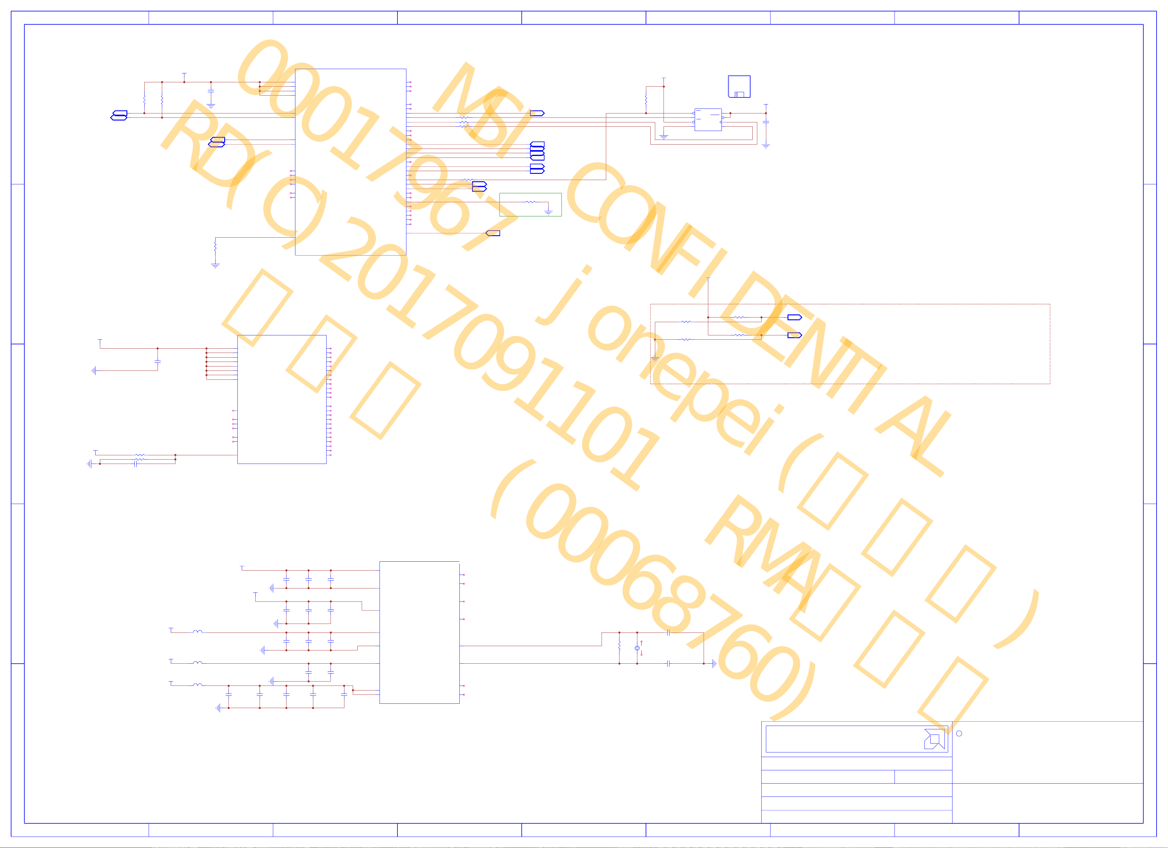
9
9
A
B
C
D
E
8
7
7 46 5 123
DOCUMENT NUMBER:
TITLE:
C
is provided only to entities under a non-disclosure agreement with AMD
NOTES:
2
OF
REV:
4
D
1
A
B
58 6 3
SHEET:
SHEET NUMBER:
DATE:
This AMD Board schematic and design is the exclusive property of AMD, and
Advanced Micro Devices
CONFIDENTIAL AND PROPRIETARY TO ADVANCED MICRO DEVICES INC.
information included herein.
responsibility for any consequences resulting from use of the
of merchantability or fitness for a particular purpose, and disclaims
schematic and design, including, not limited to, any implied warranty
AMD makes no representations or warranties of any kind regarding this
evaluation requires a Board Technology License Agreement with AMD.
prohibited. Use of this schematic and design for any purpose other than
for evaluation purposes. Further distribution or disclosure is strictly
C
E
ININOUT
OUT
IN
DP_VDDR
DP_VDDC
XTALOUT
XTALIN
XO_IN2
XO_IN
SPLL_VDDC
SPLL_PVSS
SPLL_PVDD
NC_XTAL_PVSS
NC_XTAL_PVDD
MPLL_PVDD
MPLL_PVDD
DP_VSSR
CLKTESTB
CLKTESTA
DBG_VREFG
VDDR4
VDDR4
VDDR4
VDDR4
VDDR4
VDDR4
VDDR4
VDDR4
NC#5
NC#4
NC#3
NC#2
NC#1
DBG_DATA9
DBG_DATA8
DBG_DATA7
DBG_DATA6
DBG_DATA5
DBG_DATA4
DBG_DATA3
DBG_DATA23
DBG_DATA22
DBG_DATA21
DBG_DATA20
DBG_DATA2
DBG_DATA19
DBG_DATA18
DBG_DATA17
DBG_DATA16
DBG_DATA15
DBG_DATA14
DBG_DATA13
DBG_DATA12
DBG_DATA11
DBG_DATA10
DBG_DATA1
DBG_DATA0
DBG_CNTL0
VDDR3
VDDR3
VDDR3
VDDR3
RSVD#AK27
TEST_PG
SMBDATA
SMBCLK
SDA
SCL
NC#75
NC#74
NC#73
NC#72
HPD1
GPIO_9_ROMSI
GPIO_8_ROMSO
GPIO_7_BLON
GPIO_6_TACH
GPIO_5_AC_BATT
GPIO_30
GPIO_29
GPIO_22_ROMCSB
GPIO_21
GPIO_20_PWRCNTL_1
GPIO_2
GPIO_19_CTF
GPIO_18_HPD3
GPIO_17_THERMAL_INT
GPIO_16
GPIO_15_PWRCNTL_0
GPIO_14_HPD2
GPIO_13
GPIO_12
GPIO_11
GPIO_10_ROMSCK
GPIO_1
GPIO_0
GENERICG_HPD6
GENERICF_HPD5
GENERICE_HPD4
GENERICD
GENERICC
GENERICB
GENERICA
RSVD#AJ27
CLKREQB
OUT
BIOS
OUT
OUT
OUT
OUT
OUT
OUTBIBI
OUT
OUT
CE
SI
SCK
HOLD
VDD
GND
WP
SO
9
MSI CONFIDENTIAL
00017967 jonepei(裴亮樂)
RD(C)2017091101 RMA工程課
石阿鋒 (00068760)
8
7 46 5 123
OLAND GPIOs Strap CF XTAL OSC
OLAND GPIOs Strap CF XTAL OSC
+3.3V_BUS
+3.3V_BUS
R4018R4017
R4018
R4017
4.7K 4.7K
E
18 16
18 16
18 16
18 16
OUT
BI
4.7K 4.7K
2 1
2 1
2 1
2 1
D
C1
C1
1uF
1uF
6.3V
6.3V
2 1
2 1
1
1
OUT
1
1
BI
R33
R33
1K
1K
2 1
2 1
60mA
60mA
SMBCLK
SMBCLK
SMBDATA
SMBDATA
TEST_PG
TEST_PG
SCL
SCL
SDA
SDA
AF23
AF23
AF24
AF24
AG23
AG23
AG24
AG24
AK26
AK26
AJ26
AJ26
AJ23
AJ23
AH23
AH23
AF35
AF35
AG36
AG36
AJ27
AJ27
AK27
AK27
AN36
AN36
AP37
AP37
AH16
AH16
VDDR3
VDDR3
VDDR3
VDDR3
SCL
SDA
SMBCLK
SMBDATA
NC#75
NC#74
RSVD#AJ27
RSVD#AK27
NC#73
NC#72
TEST_PG
PN 2280007900G for 1Mbit (PM25LV010A-100SCE)
U1
U1
OLAND M2 GDDR5
OLAND M2 GDDR5
GPIO_0
GPIO_1
GPIO_2
GPIO_5_AC_BATT
GPIO_10_ROMSCK
GPIO_15_PWRCNTL_0
GPIO_17_THERMAL_INT
GPIO_20_PWRCNTL_1
GPIO_22_ROMCSB
GPIO_6_TACH
GPIO_7_BLON
GPIO_8_ROMSO
GPIO_9_ROMSI
GPIO_11
GPIO_12
GPIO_13
GPIO_14_HPD2
GPIO_16
GPIO_18_HPD3
GPIO_19_CTF
GPIO_21
GPIO_29
GPIO_30
CLKREQB
GENERICA
GENERICB
GENERICC
GENERICD
GENERICE_HPD4
GENERICF_HPD5
GENERICG_HPD6
HPD1
AH20
AH20
AH18
AH18
AN16
AN16
AH17
AH17
AJ17
AJ17
AK17
AK17
AJ13
AJ13
AH15
AH15
AJ16
AJ16
AK16
AK16
AL16
AL16
AM16
AM16
AM14
AM14
AM13
AM13
AK14
AK14
AG30
AG30
AN14
AN14
AM17
AM17
AL13
AL13
AJ14
AJ14
AK13
AK13
AG32
AG32
AG33
AG33
AN13
AN13
AJ19
AJ19
AK19
AK19
AJ20
AJ20
AK20
AK20
AJ24
AJ24
AH26
AH26
AH24
AH24
AK24
AK24
GPIO_8
GPIO_8
GPIO_9
GPIO_9
GPIO_10
GPIO_10
GPIO_22
GPIO_22
GPIO_29_VID2
GPIO_29_VID2
GPIO_30_VID3
GPIO_30_VID3
HPD1
HPD1
GPIO_7_VDDCI_VID0 GPIO_22_R
GPIO_7_VDDCI_VID0 GPIO_22_R
63
63
RP1
RP1
33R
33R
33R
33R
RP1
RP1
81
81
72
72
RP1
RP1
33R
33R
GPIO_14_HPD2
GPIO_14_HPD2
GPIO_15_VID0
GPIO_15_VID0
GPIO_16_VDDCI_VID1
GPIO_16_VDDCI_VID1
GPIO_17_THERMINT
GPIO_17_THERMINT
GPIO_19_CTF
GPIO_19_CTF
GPIO_20_VID1
GPIO_20_VID1
54
54
RP1
RP1
33R
33R
16
16
OUT
16
16
OUT
GENERICB
GENERICB
IN
CONNECT AT ASIC
CONNECT AT ASIC
R32
7
7
DNI
DNI
OUT
IN
OUT
OUT
IN
OUT
OUT
16
16
9
9
16
16
16
16
18
18
17
17
16
16
CLKREQ# requires open drain connection,
CLKREQ# requires open drain connection,
10K
10K
21
21R32
and cannot be used as pinstrap
and cannot be used as pinstrap
GPIO_8_R
GPIO_8_R
PN 2280007900G for 1Mbit (PM25LV010A-100SCE)
BIOS1
BIOS(113?)
BIOS(113?)
8
8
7
7
6
6
5
5
SI
GPIO_9_R
GPIO_9_R
BIOS1
BIOS
+3.3V_BUS
+3.3V_BUS
+3.3V_BUS
+3.3V_BUS
R14
R14
4.7K
4.7K
2 1
2 1
VIDEO BIOS
VIDEO BIOS
FIRMWARE
FIRMWARE
U11
U11
1
1
CE
2
2
SO
3
3
WP
4
4
GND
PM25LD010C-SCE
PM25LD010C-SCE
VDD
HOLD
SCK
GPIO_10_R
GPIO_10_R
C4
C4
0.1uF
0.1uF
6.3V
6.3V
2 1
2 1
PIN BASED STRAPS
PIN BASED STRAPS
E
D
+3.3V_BUS
DNI
DNI
MR10
MR10
U1
U1
+1.8V
+1.8V
AU1
AF15
AF15
180mA
180mA
10mA/bit
10mA/bit
C6
C6
1uF
1uF
6.3V
6.3V
2 1
2 1
C
+1.8V
+1.8V
R17
R17
R18
R18
C8
C8
1%
1%
21
21
1%
1%
6.3V
6.3V
221R
221R
21
21
110R
110R
21
21
0.1uF
0.1uF
VREFG
VREFG
VDDR4
AG11
AG11
VDDR4
AG13
AG13
VDDR4
AD12
AD12
VDDR4
AF11
AF11
VDDR4
AG15
AG15
VDDR4
AF12
AF12
VDDR4
AF13
AF13
VDDR4
AR1
AR1
NC#1
AP8
AP8
DBG_CNTL0
AW8
AW8
NC#2
AR3
AR3
NC#3
AR8
AR8
NC#4
AU8
AU8
NC#5
AH13 AP12
AH13 AP12
DBG_VREFG
OLAND M2 GDDR5
OLAND M2 GDDR5
DBG_DATA0
DBG_DATA1
DBG_DATA2
DBG_DATA3
DBG_DATA4
DBG_DATA5
DBG_DATA6
DBG_DATA7
DBG_DATA8
DBG_DATA9
DBG_DATA10
DBG_DATA11
DBG_DATA12
DBG_DATA13
DBG_DATA14
DBG_DATA15
DBG_DATA16
DBG_DATA17
DBG_DATA18
DBG_DATA19
DBG_DATA20
DBG_DATA21
DBG_DATA22
DBG_DATA23
AU1
AU3
AU3
AW3
AW3
AP6
AP6
AW5
AW5
AU5
AU5
AR6
AR6
AW6
AW6
AU6
AU6
AT7
AT7
AV7
AV7
AN7
AN7
AV9
AV9
AT9
AT9
AR10
AR10
AW10
AW10
AU10
AU10
AP10
AP10
AV11
AV11
AT11
AT11
AR12
AR12
AW12
AW12
AU12
AU12
DNI
DNI
MR11
MR11
+3.3V_BUS
4.7K
4.7K
21
21
4.7K
4.7K
21
21
DNI
DNI
R10
R10
R11
R11
4.7K
4.7K
21
21
4.7K
4.7K
21
21
V1SYNC
V1SYNC
H1SYNC
H1SYNC
OUT
OUT
AUD[1:0]:
9 6
9 6
9 6
9 6
AUD[1] HSYNC
AUD[1] HSYNC
AUD[0]
AUD[0]
VSYNC
VSYNC
AUD[1:0]:
00 - No audio function;
00 - No audio function;
01 - Audio for DisplayPort only;
01 - Audio for DisplayPort only;
10 - Audio for DisplayPort and HDMI if dongle is detected;
10 - Audio for DisplayPort and HDMI if dongle is detected;
11 - Audio for both DisplayPort and HDMI.
11 - Audio for both DisplayPort and HDMI.
HDMI must only be enabled on systems that are legally entitled
HDMI must only be enabled on systems that are legally entitled
. It is the responsibility of the system designer to
. It is the responsibility of the system designer to
ensure that the system is entitled to support this feature
ensure that the system is entitled to support this feature
C
B
A
Place the crossfire
Place the crossfire
testpoints near the ASIC and
testpoints near the ASIC and
not the connector
not the connector
Please pay attention to the grounding
Please pay attention to the grounding
strategies for these filter capacitors to
strategies for these filter capacitors to
maintain a close loop for current.
maintain a close loop for current.
+1.8V
+1.8V
+1.8V
+1.8V
+0.95V
+0.95V
9
+1.8V
+1.8V
B5
B5
120R
120R
B6
B6
120R
120R
B7
B7
120R
120R
21
21
21
21
21
21
C24
C24
10uF
10uF
6.3V
6.3V
2 1
2 1
150mA
150mA
200mA
200mA
75mA
75mA
+0.95V
+0.95V
140mA
140mA
75mA
75mA
+SPV10
+SPV10
C34
C34
4.7uF
4.7uF
6.3V
6.3V
2 1
2 1
2 1
2 1
C31
4.7uF
4.7uF
6.3V
6.3V
2 1
2 1
C18
4.7uF
4.7uF
6.3V
6.3V
2 1
2 1
2 1
2 1
C13
C13
10uF
10uF
6.3V
6.3V
C35
C35
4.7uF
4.7uF
6.3V
6.3V
2 1
2 1
C16
1uF
1uF
6.3V
6.3V
2 1
2 1
C19C18
C19
1uF
1uF
6.3V
6.3V
2 1
2 1
2 1
2 1
C14
C14
1uF
1uF
6.3V
6.3V
C21
C21
1uF
1uF
6.3V
6.3V
2 1
2 1
+SPV18
+SPV18
C26
C26
1uF
1uF
6.3V
6.3V
2 1
2 1
C17C16C31
C17
0.1uF
0.1uF
6.3V
6.3V
2 1
2 1
2 1
2 12 1
2 1
7
C15
C15
0.1uF
0.1uF
6.3V
6.3V
C20
C20
0.1uF
0.1uF
6.3V
6.3V
C22
C22
0.1uF
0.1uF
6.3V
6.3V
2 1
2 1
C27
C27
0.1uF
0.1uF
6.3V
6.3V
AM32
AM32
AN32
AN32
AM10
AM10
AN10
AN10
AN9
AN9
AN31
AN31
H7
H7
H8
H8
DP_VDDR
DP_VSSR
DP_VDDC
SPLL_PVDD
SPLL_PVSS
SPLL_VDDC
MPLL_PVDD
MPLL_PVDD
U1
U1
OLAND M2 GDDR5
OLAND M2 GDDR5
NC_XTAL_PVDD
NC_XTAL_PVSS
XO_IN2
XO_IN
XTALIN
XTALOUT
CLKTESTA
CLKTESTB
AF30
AF30
AF31
AF31
AW35
AW35
AW34
AW34
AV33
AV33
AU34
AU34
AK10
AK10
AL10
AL10
XTALIN
XTALIN
XTALOUT
XTALOUT
1st source: 502G270001G
1st source: 502G270001G
R37
R37
1M
1M
1%
1%
2 1
2 1
Y1
Y1
3
42
3
42
1
1
C45
27.000MHz
27.000MHz
C23
21C45
21
21C23
21
58 6 3
12pF
12pF
12pF
12pF
50V
50V
50V
50V
AMD - PLATFORM HARDWARE ENG
AMD - PLATFORM HARDWARE ENG
#48, No.1387, ZHANGDONG ROAD
#48, No.1387, ZHANGDONG ROAD
SHANGHAI, CHINA 201203
SHANGHAI, CHINA 201203
Oland GPIO STRAP PLL
SHEET:
DATE:
SHEET NUMBER:
DOCUMENT NUMBER:
NOTES:
4
Oland GPIO STRAP PLL
Fri Oct 28 17:09:38 2016
Fri Oct 28 17:09:38 2016
NOTE
NOTE
215
OF
105_CXXX00_00A
105_CXXX00_00A
215
REV:
1.0
1.0
CONFIDENTIAL AND PROPRIETARY TO ADVANCED MICRO DEVICES INC.
Advanced Micro Devices
2016
2016
C
This AMD Board schematic and design is the exclusive property of AMD, and
is provided only to entities under a non-disclosure agreement with AMD
for evaluation purposes. Further distribution or disclosure is strictly
prohibited. Use of this schematic and design for any purpose other than
evaluation requires a Board Technology License Agreement with AMD.
AMD makes no representations or warranties of any kind regarding this
schematic and design, including, not limited to, any implied warranty
of merchantability or fitness for a particular purpose, and disclaims
responsibility for any consequences resulting from use of the
information included herein.
TITLE:
2
TITLE
TITLE
1
B
A
Page 6
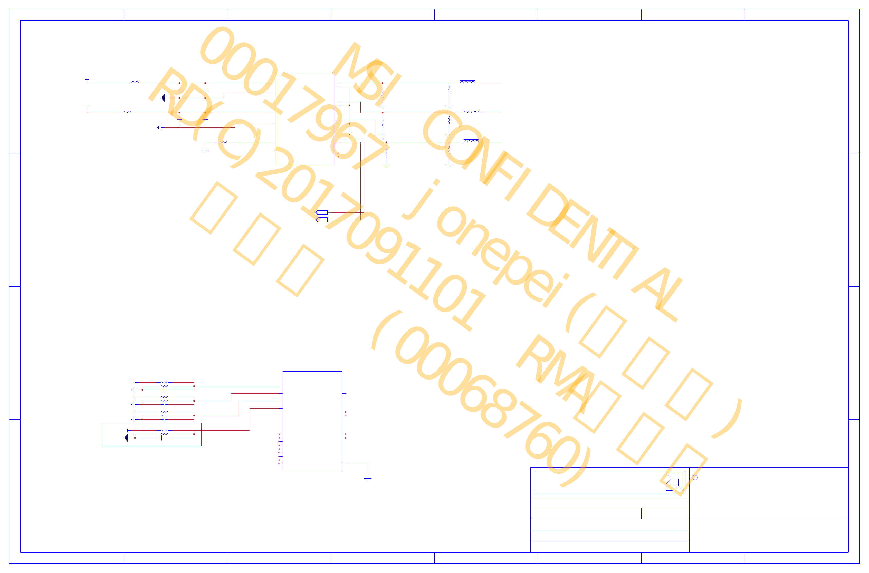
DOCUMENT NUMBER:
TITLE:
17ci203
C
is provided only to entities under a non-disclosure agreement with AMD
NOTES:
2
OF
REV:
4
A
C
D D
1
1
A
B B
C
5
8
8
7
7
6
6
5 4 3
3
2
SHEET:
SHEET NUMBER:
DATE:
This AMD Board schematic and design is the exclusive property of AMD, and
Advanced Micro Devices
CONFIDENTIAL AND PROPRIETARY TO ADVANCED MICRO DEVICES INC.
information included herein.
responsibility for any consequences resulting from use of the
of merchantability or fitness for a particular purpose, and disclaims
schematic and design, including, not limited to, any implied warranty
AMD makes no representations or warranties of any kind regarding this
evaluation requires a Board Technology License Agreement with AMD.
prohibited. Use of this schematic and design for any purpose other than
for evaluation purposes. Further distribution or disclosure is strictly
SWAPLOCKB
SWAPLOCKA
PS_3
PS_2
PS_1
PS_0
NC_SVI2
NC_SVI2
NC_SVI2
NC#39
NC#28
NC#27
NC#26
NC#25
NC#24
NC#23
GENLK_VSYNC
GENLK_CLK
CEC_1
OUT
VSYNC
VSS1DI
VDD1DI
RSET
R
HSYNC
G
DDCVGADATA
DDCVGACLK
B
AVSSQ AVSSN
AVSSN
AVSSN
AVDD
OUT
8
MSI CONFIDENTIAL
00017967 jonepei(裴亮樂)
RD(C)2017091101 RMA工程課
石阿鋒 (00068760)
7
6
5 4 3
2
1
See BOM for qualified filters
See BOM for qualified filters
Pseudo differential RGB should be routed from the ASIC to the display
Pseudo differential RGB should be routed from the ASIC to the display
connector without switching reference plane or running over split plane.
U1
+1.8V
+1.8V
D D
+1.8V
+1.8V
B1700
B1700
2 1
2 1
120R
120R
B1701
B1701
2 1
2 1
120R
120R
+AVDD_DAC1
+AVDD_DAC1
C1700
C1702
C1702
AC33
+VDD1DI
+VDD1DI
C1701C1700
C1701
1uF
1uF
6.3V
6.3V
2 1
2 1
C1703
C1703
1uF
1uF
6.3V
6.3V
2 1
2 1
2 1
2 1
2 1
2 1
0.1uF
0.1uF
6.3V
6.3V
0.1uF
0.1uF
6.3V
6.3V
R1700
R1700
499R
499R
1%
1%
RSET
RSET
21
21
AC33
VDD1DI
AC34
AC34
VSS1DI
AD34
AD34
AVDD
AE34 AE38
AE34 AE38
AVSSQ AVSSN
AB34
AB34
RSET
U1
OLAND M2 GDDR5
OLAND M2 GDDR5
AVSSN
AVSSN
HSYNC
VSYNC
DDCVGACLK
DDCVGADATA
AD39
AD39
R
AD37
AD37
AE36
AE36
G
AD35
AD35
G_DAC1
G_DAC1
AF37
AF37
B
AC36
AC36
AC38
AC38
AJ30
AJ30
AJ31
AJ31
B_DAC1
B_DAC1
R1711
R1711
150R
150R
1%
1%
2 1
2 12 1
R1712
R1712
150R
150R
1%
1%
2 1
VGA
VGA
VGA
VGA
R1713
R1713
150R
150R
1%
1%
2 1
2 1
VGA
VGA
connector without switching reference plane or running over split plane.
VGA(3230000000G)
VGA(3230000000G)
L1710
VGA
VGA
R1701
R1701
150R
150R
1%
1%
2 1
2 1
VGA
VGA
R1702
R1702
150R
150R
1%
1%
2 1
2 1
VGA(3230000000G)
VGA(3230000000G)
VGA
VGA
R1703
R1703
150R
150R
1%
1%
2 1
2 1
L1710
0.047uH
0.047uH
VGA(3230000000G)
VGA(3230000000G)
0.047uH
0.047uH
0.047uH
0.047uH
L1711
L1711
L1712
L1712
21
21
21
21
21
21
A_R_DAC1R_DAC1
A_R_DAC1R_DAC1
A_G_DAC1
A_G_DAC1
A_B_DAC1
A_B_DAC1
9
9
9
9
9
9
C
9 5
9 5
9 5
9 5
OUT
OUT
H1SYNC
H1SYNC
V1SYNC
V1SYNC
B B
U1
PCIE3.0 Support: R1054=2K, R1053=8.45K
PCIE3.0 Support: R1054=2K, R1053=8.45K
PCIE2.0 Support: R1054=4.75K,R1053=NC
PCIE2.0 Support: R1054=4.75K,R1053=NC
DNI
DNI
DNI
DNI
21R1051
21
21R1052
21
21C1052
21
0.082uF
0.082uF
21R1053
21
21R1054
21
21C1054
21
0.1uF
0.1uF
21R1055
21
21R1056
21
21C1056
21
0.68uF
0.68uF
+1.8V
+1.8V
+1.8V
+1.8V
+1.8V
+1.8V
R1051
R1052
C1052
R1053
R1054
C1054
R1055
R1056
C1056
5.1K
5.1K
16V
16V
6.3V
6.3V
4V
4V
1%3.24K
1%3.24K
1%5.62K
1%5.62K
1%8.45k
1%8.45k
1%2K
1%2K
1%4.75K
1%4.75K
PS_0
PS_0
PS_1
PS_1
PS_2
PS_2
AM34
AM34
AD31
AD31
AG31
AG31
AD33
AD33
PS_0
PS_1
PS_2
PS_3
U1
CEC_1
GENLK_CLK
GENLK_VSYNC
AC30
AC30
AD29
AD29
AC29
AC29
C
A
1%8.45K
DNI
DNI
+1.8V
+1.8V
MEM CONFIG ID: SEE MLPS Bit[3:1]
MEM CONFIG ID: SEE MLPS Bit[3:1]
PS_3[3:1] PU[R1057] PD[R1058]
PS_3[3:1] PU[R1057] PD[R1058]
000 NC 4.75K_3160475100G
000 NC 4.75K_3160475100G
001 8.45K_3160845100G 2.00K_3160200100G
001 8.45K_3160845100G 2.00K_3160200100G
010 4.53K_3160453100G 2.00K_3160200100G
010 4.53K_3160453100G 2.00K_3160200100G
011 6.98K_3160398100G 4.99K_3160499100G
011 6.98K_3160398100G 4.99K_3160499100G
100 4.53_3160453100G 4.99K_3160499100G
100 4.53_3160453100G 4.99K_3160499100G
101 3.24K_3160324100G 5.62K_3160562100G
101 3.24K_3160324100G 5.62K_3160562100G
110 3.40K_3160340100G 10.0K_3160100200G
110 3.40K_3160340100G 10.0K_3160100200G
111 4.75K_3160475100G NC
111 4.75K_3160475100G NC
R1057
R1058
C1058
21R1057
21
21R1058
21
21C1058 AK21
21 AK21
0.082uF
0.082uF
DNI
DNI
8
1%8.45K
1%4.75K
1%4.75K
16V
16V
7
PS_3
PS_3
AF32
AF32
V13
V13
U13
U13
AG21
AG21
AC32
AC32
AA29
AA29
AC31
AC31
AD30
AD30
AD32
AD32
6
NC#25
NC#28
NC#27
NC#26
NC#24
NC#23
NC_SVI2
NC_SVI2
NC_SVI2
OLAND M2 GDDR5
OLAND M2 GDDR5
SWAPLOCKA
SWAPLOCKB
NC#39
AJ21
AJ21
AF33
AF33
CONFIDENTIAL AND PROPRIETARY TO ADVANCED MICRO DEVICES INC.
Advanced Micro Devices
2016
2016
AMD - PLATFORM HARDWARE ENG
AMD - PLATFORM HARDWARE ENG
#48, No.1387, ZHANGDONG ROAD
#48, No.1387, ZHANGDONG ROAD
SHANGHAI, CHINA 201203
SHANGHAI, CHINA 201203
SHEET:
DATE:
SHEET NUMBER:
DOCUMENT NUMBER:
NOTES:
5
4
Oland DAC and MLPS
Oland DAC and MLPS
Fri Oct 28 17:09:42 2016
Fri Oct 28 17:09:42 2016
OF
105_CXXX00_00A
105_CXXX00_00A
NOTE
NOTE
3
REV:
216
216
1.0
1.0
C
This AMD Board schematic and design is the exclusive property of AMD, and
is provided only to entities under a non-disclosure agreement with AMD
for evaluation purposes. Further distribution or disclosure is strictly
prohibited. Use of this schematic and design for any purpose other than
evaluation requires a Board Technology License Agreement with AMD.
AMD makes no representations or warranties of any kind regarding this
schematic and design, including, not limited to, any implied warranty
of merchantability or fitness for a particular purpose, and disclaims
responsibility for any consequences resulting from use of the
information included herein.
TITLE:
2
TITLE
TITLE
1
A
Page 7
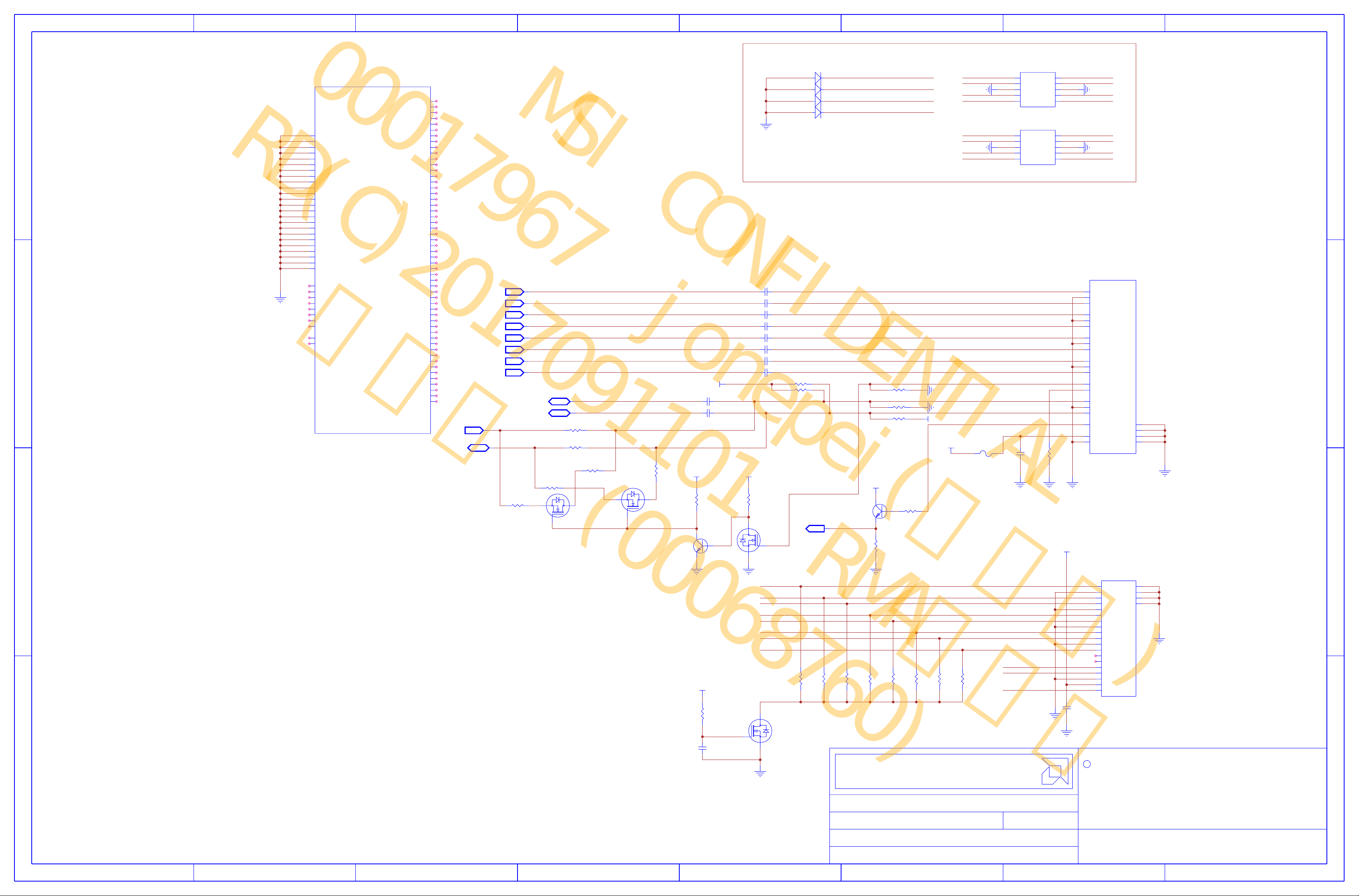
This AMD Board schematic and design is the exclusive property of AMD, and
DATE:
SHEET:
Advanced Micro Devices
2
3
345
6
6
7
7
8
8
C
5
CONFIDENTIAL AND PROPRIETARY TO ADVANCED MICRO DEVICES INC.
C
BB
A
1
DD
C
A
4
REV:
SHEET NUMBER:
DOCUMENT NUMBER:
OF
1
prohibited. Use of this schematic and design for any purpose other than
for evaluation purposes. Further distribution or disclosure is strictly
is provided only to entities under a non-disclosure agreement with AMD
2
schematic and design, including, not limited to, any implied warranty
AMD makes no representations or warranties of any kind regarding this
evaluation requires a Board Technology License Agreement with AMD.
of merchantability or fitness for a particular purpose, and disclaims
responsibility for any consequences resulting from use of the
information included herein.
TITLE:
G4
G3
G2
G1PWR_RTN
DP_PWR
AUX_CHn
AUX_CHp
Hot_Det
GND_6
CONFIG 2
CONFIG 1
GND_3
GND_2
GND_1
GND_0
ML_Lane_3n
ML_Lane_2n
ML_Lane_1n
ML_Lane_0n
ML_Lane_3p
ML_Lane_2p
ML_Lane_1p
ML_Lane_0p
Y4
Y3
GND1
Y2
Y1
D
C
A
GND
B
Y4
Y3
GND1
Y2
Y1
D
C
A
GND
B
CASE
CASE
CASE
CASE
P19
P18
P17
P16
P15
P14
P13
P12
P11
P10
P9
P8
P7
P6
P5
P4
P3
P2
P1
OUTININININININBIININBIINBI
NC#AW18
NC#AW28
NC#AK29
NC#AM21
NC#AM29
NC#AM30
NC#AK30
NC#AN21
NC#AL29
NC#AL30
NC#71
NC#70
NC#69
NC#68
NC#67
NC#66
NC#65
NC#64
NC#63
NC#62
NC#61
NC#60
NC#59
NC#58
NC#57
NC#56
NC#55
NC#54
NC#53
NC#52
NC#51
NC#50
NC#49
NC#48
NC#47
NC#46
NC#45
NC#44
NC#43
NC#42
NC#41
NC#40
NC#32
NC#31
NC#30
NC#29
NC#22
NC#21
NC#20
NC#19
NC#18
NC#17
NC#16
NC#15
NC#14
NC#13
NC#12
NC#11
NC#10
NC#9
NC#8
NC#7
NC#6
DP_VSS
DP_VSS
DP_VSS
DP_VSS
DP_VSS
DP_VSS
DP_VSS
DP_VSS
DP_VSS
DP_VSS
DP_VSS
DP_VSS
DP_VSS
DP_VSS
DP_VSS
DP_VSS
DP_VSS
DP_VSS
DP_VSS
DP_VSS
DP_VSS
DP_VSS
DP_VSS
DP_VSS
8
MSI CONFIDENTIAL
00017967 jonepei(裴亮樂)
RD(C)2017091101 RMA工程課
石阿鋒 (00068760)
7
6
345
2
1
C
A
8
U1
U1
AN17
AN17
DP_VSS
AN19
AN19
DP_VSS
AN27
AN27
DP_VSS
AN29
AN29
DP_VSS
AP16
AP16
DP_VSS
AP17
AP17
DP_VSS
AP18
AP18
DP_VSS
AP19
AP19
DP_VSS
AP27
AP27
DP_VSS
AP28
AP28
DP_VSS
AP29
AP29
DP_VSS
AP30
AP30
DP_VSS
AR18
AR18
DP_VSS
AR28
AR28
DP_VSS
AV17
AV17
DP_VSS
AV27
AV27
DP_VSS
AW14
AW14
DP_VSS
AW16
AW16
DP_VSS
AW20
AW20
DP_VSS
AW22
AW22
DP_VSS
AW24
AW24
DP_VSS
AW26
AW26
DP_VSS
AW30
AW30
DP_VSS
AW32
AW32
DP_VSS
AL30
AL30
NC#AL30
AL29
AL29
NC#AL29
AN21
AN21
NC#AN21
AK30
AK30
NC#AK30
AM30
AM30
NC#AM30
AM29
AM29
NC#AM29
AM21
AM21
NC#AM21
AK29
AK29
NC#AK29
AW28
AW28
NC#AW28
AW18
AW18
NC#AW18
OLAND M2 GDDR5
OLAND M2 GDDR5
7
D2500
D2500
D2501
D2501
D2502
21C3530
21
21C3531
21
21C3532
21
21C3533
21
21C3534
21
21C3536
21
21C3537
21
21C3538
21
R2701
R2703
DP
DP
Q1804
Q1804
2N7002E
2N7002E
1
1
DPA_GND
DPA_GND
Q2701
Q2701
2N7002E
2N7002E
HDMI
HDMI
D2502
D2505
D2505
0.1uF
0.1uF
0.1uF
0.1uF
0.1uF
0.1uF
0.1uF
0.1uF
0.1uF
0.1uF
0.1uF
0.1uF
0.1uF
0.1uF
0.1uF
0.1uF
DP;HDMI
DP;HDMI
6.3V
6.3V
DP;HDMI
DP;HDMI
6.3V
6.3V
DP;HDMI
DP;HDMI
6.3V
6.3V
DP;HDMI
DP;HDMI
6.3V
6.3V
DP;HDMI
DP;HDMI
6.3V
6.3V
DP;HDMI
DP;HDMI
6.3V
6.3V
DP;HDMI
DP;HDMI
6.3V
6.3V
DP;HDMI
DP;HDMI
6.3V
6.3V
HDMI
HDMI
HDMI
HDMI
DPA_DONGLE_DET
DPA_DONGLE_DET
7
7
5
5
R2713
499R1%499R1%499R1%499R1%499R1%499R1%499R1%499R
499R1%499R1%499R1%499R1%499R1%499R1%499R1%499R
1%
HDMI HDMI HDMI HDMI HDMI HDMI HDMI HDMI
1%
HDMI HDMI HDMI HDMI HDMI HDMI HDMI HDMI
2 1
2 1
AH12
AH12
NC#6
AP13
AP13
NC#7
AP14
AP14
NC#8
AP15
AP15
NC#9
AT13
AT13
NC#10
AN24
AN24
NC#11
AP20
AP20
NC#12
AP21
AP21
NC#13
AP22
AP22
NC#14
AP23
AP23
NC#15
AP24
AP24
NC#16
AP25
AP25
NC#17
AP26
AP26
NC#18
AU18
AU18
NC#19
AU28
AU28
NC#20
AV19
AV19
NC#21
AV29
AV29
NC#22
L27
L27
NC#29
N12
N12
NC#30
AG12
AG12
NC#31
M12
M12
NC#32
AR24
AR24
NC#40
AR14
AR14
NC#41
AT25
AT25
NC#42
AT15
AT15
NC#43
AV25
AV25
NC#44
AV15
AV15
NC#45
AU26
AU26
NC#46
AU16
AU16
NC#47
AR26
AR26
NC#48
AR16
AR16
NC#49
AT27
AT27
NC#50
AT17
AT17
NC#51
AU30
NC#52
NC#53
NC#54
NC#55
NC#56
NC#57
NC#58
NC#59
NC#60
NC#61
NC#62
NC#63
NC#64
NC#65
NC#66
NC#67
NC#68
NC#69
NC#70
NC#71
6
AU30
AR20
AR20
AV31
AV31
AT21
AT21
AT31
AT31
AV21
AV21
AR32
AR32
AU22
AU22
AU32
AU32
AR22
AR22
AT33
AT33
AT23
AT23
AV23
AV23
AU24
AU24
AT29
AT29
AR30
AR30
AV13
AV13
AU14
AU14
AT19
AT19
AU20
AU20
8
8
IN
8
8
IN
8
8
IN
8
8
IN
8
8
IN
8
8
IN
DPA_A3P
21
21
1
1
8
8
8
8
R2528
R2529
DPA_A3P
BI
BI
DP;HDMI
DP;HDMI
MR2529
MR2529
0R
0R
2
2
DNI
DNI
DNI
DNI
21
21
Q1801
Q1801
2N7002DW
2N7002DW
6
6
AUX2P
AUX2P
AUX2N
AUX2N
0R
0R
21R2528
21
0R
0R
21R2529
21
DP;HDMI
DP;HDMI
MMR2528
MMR2528
0R
0R
+5V_VESA
+5V_VESA
C3535
C3541
MMR2529
21
21
MMR2529
4
4
5
5
DP;HDMI
DP;HDMI
0R
0R
Q1801
Q1801
2 1
2 1
2N7002DW
2N7002DW
DP;HDMI
DP;HDMI
3
3
AUX1_BYPSS_EN
AUX1_BYPSS_EN
MMBT3904
MMBT3904
+12V_BUS
+12V_BUS
Q1803
Q1803
DP
DP
+12V_BUS
+12V_BUS
R1804
R1804
10K
10K
DP;HDMI
DP;HDMI
2 12 3
2 1
2 3
R2344
R2344
10K
10K
HDMI
HDMI
2 1
2 1
2 1 2 1
TMDP_EN
TMDP_EN
C2344
C2344
0.1uF
0.1uF
16V
16V
8
8
IN
8
8
IN
DDC2CLK
8
8
IN
8
8
BI
DDC2CLK
DDC2DATA
DDC2DATA
DP;HDMI DP;HDMI
DP;HDMI DP;HDMI
MR2528
MR2528
0R
0R
5
21C3535
21
6.3V
6.3V
21C3541
21
6.3V
6.3V
1
1
0.1uF
0.1uF
0.1uF
0.1uF
C3530
C3531
C3532
C3533
C3534
C3536
C3537
C3538
DP
DP
DP
DP
+12V_BUS
+12V_BUS
R1805
R1805
10K
10K
DP
DP
2 1
2 12
3
3
2
1
1
7
7
7
7
7
7
7
7
7
7
7
7
7
7
7
7
3
3
2
2
4
ESD5V3U1U-02LRH
ESD5V3U1U-02LRH
12
12
ESD5V3U1U-02LRH
ESD5V3U1U-02LRH
12
12
ESD5V3U1U-02LRH
ESD5V3U1U-02LRH
12
12
ESD5V3U1U-02LRH
ESD5V3U1U-02LRH
12
12
2.2K
2.2K
21R2701
21
2.2K
2.2K
21R2703
21
Q2513
Q2513
MMBT3904 10K
MMBT3904 10K
DP;HDMI
DP;HDMI
HPD1
HPD1
OUT
R2715
R2714
2 1
2 1
2 1
2 1
AMD - PLATFORM HARDWARE ENG
AMD - PLATFORM HARDWARE ENG
#48, No.1387, ZHANGDONG ROAD
#48, No.1387, ZHANGDONG ROAD
SHANGHAI, CHINA 201203
SHANGHAI, CHINA 201203
SHEET:
DATE:
SHEET NUMBER:
DOCUMENT NUMBER:
R2524
DPA_AUXP
7
7
DPA_AUXP
R2522
DPA_AUXN
7
7
DPA_AUXN
R2523
+3.3V_BUS
+3.3V_BUS
2 3
2 3
R2530
R2530
10K
10K
DP;HDMI
DP;HDMI
2 1
2 1
R2716
2 1
2 1
Oland Connector HDMI/DP
Oland Connector HDMI/DP
Fri Oct 28 17:09:39 2016 1.0
Fri Oct 28 17:09:39 2016 1.0
OPTIONAL ESD protection diodes
OPTIONAL ESD protection diodes
DPA_AUXN
DPA_AUXN
DPA_AUXP
DPA_AUXP
DPA_DONGLE_DET
DPA_DONGLE_DET
HPD_DPA
HPD_DPA
DP
DP
DP
DP
DP
DP
2 1R2523
2 1
R2527
R2527
1
1
R2717
2 1
2 1
7 21
7 21
21R2524
21
21R2522
21
7
7
7
7
7
7
7
7
DPA_0PDPA_A0P
DPA_0PDPA_A0P
7
7
DPA_0NDPA_A0N
DPA_0NDPA_A0N
7
7
DPA_1PDPA_A1P
DPA_1PDPA_A1P
7
7
DPA_1NDPA_A1N
DPA_1NDPA_A1N
7
7
DPA_2PDPA_A2P
DPA_2PDPA_A2P
7
7
DPA_2NDPA_A2N
DPA_2NDPA_A2N
7
7
DPA_3P
DPA_3P
7
7
DPA_3NDPA_A3N
7
7
DPA_3NDPA_A3N
1M
1M
100K
100K
100K
100K
+3.3V_BUS
+3.3V_BUS
+3.3V_BUS
+3.3V_BUS
HPD_DPA
7
7
HPD_DPA
21
21
DP;HDMI
DP;HDMI
R2719
R2718
2 1
2 1
2 1
2 1
OF
105_CXXX00_00A
105_CXXX00_00A
3
DPA_3N
DPA_3N
7
7
DPA_3P
DPA_3P
7
7
DPA_2N
DPA_2N
7
7
DPA_2P
DPA_2P
7
7
DPA_1N
DPA_1N
7
7
DPA_1P
DPA_1P
7
7
DPA_0N
DPA_0N
7
7
DPA_0P
DPA_0P
7
7
DPA_0P
DPA_0P
R2720
R2720R2719R2718R2717R2716R2715R2714R2713
2 1
2 1
DPA_0N
DPA_0N
F2501
F2501
1.5A
1.5A
DPA_1P
DPA_1P
DPA_1N
DPA_1N
+3.3V_DPA
+3.3V_DPA
DP
DP
21
21
DPA_2P
DPA_2P
7
7
7
7
7
7
1
1
A
2
2
B
GND
4
4
C
5
5
D
RCLAMP0524P
RCLAMP0524P
1
1
A
2
2
B
GND
4
4
C
5
5
D
RCLAMP0524P
RCLAMP0524P
C2540
22uF
22uF
6.3V
6.3V
2 1
2 1
DP
DP
DPA_2N
DPA_2N
DPA_3P
DPA_3P
DPA_AUXP
DPA_AUXP
DPA_AUXN
DPA_AUXN
HPD_DPA
HPD_DPA
OVERLAP HDMI WITH DP D
OVERLAP HDMI WITH DP D
REV:
D2506
D2506
D2504
D2504
DPA_3N
DPA_3N
GND1
GND1
DPA_3N
Y1
Y2
Y3
Y4
Y1
Y2
Y3
Y4
DPA_1M
DPA_1M
R2526C2540
R2526
5.1M
5.1M
DP
DP
2 1
2 1
+5V_VESA
+5V_VESA
10
10
9
9
83
83
7
7
6
6
10
10
9
9
83
83
7
7
6
6
2 1
2 1
DPA_3N
7
7
DPA_3P
DPA_3P
7
7
DPA_2N
DPA_2N
7
7
DPA_2P
DPA_2P
7
7
DPA_1N
DPA_1N
7
7
DPA_1P
DPA_1P
7
7
DPA_0N
DPA_0N
7
7
DPA_0P
DPA_0P
7
7
DP
DP
J2501
J2501
1
1
ML_Lane_0p
2
2
GND_0
3
3
ML_Lane_0n
4
4
ML_Lane_1p
5
5
GND_1
6
6
ML_Lane_1n
7
7
ML_Lane_2p
8
8
GND_2
9
9
ML_Lane_2n
10
10
ML_Lane_3p
11
11
GND_3
12
12
ML_Lane_3n
13
13
CONFIG 1
14
14
CONFIG 2
15
15
AUX_CHp
16
16
GND_6
17
17
AUX_CHn
G4
18
18
Hot_Det
20
20
DP_PWR
19
19
DP_W/GASKET
DP_W/GASKET
DISPLAYPORT
DISPLAYPORT
HDMI
HDMI
MJ2501
MJ2501
1
1
P1
2
2
P2
3
3
P3
4
4
P4
5
5
P5
6
6
P6
7
7
P7
8
8
P8
9
9
P9
10
10
P10
11
11
P11
12
12
P12
13
13
P13
14
14
P14
15
15
P15
16
16
P16
17
17
P17
18
18
P18
19
19
P19
LONG_TYPE-2_HDMI_W/TAB
LONG_TYPE-2_HDMI_W/TAB
LONG_TYPE-2_HDMI
C2722
C2722
1uF
1uF
6.3V
6.3V
HDMI
HDMI
LONG_TYPE-2_HDMI
CONFIDENTIAL AND PROPRIETARY TO ADVANCED MICRO DEVICES INC.
2016
2016
C
This AMD Board schematic and design is the exclusive property of AMD, and
is provided only to entities under a non-disclosure agreement with AMD
for evaluation purposes. Further distribution or disclosure is strictly
prohibited. Use of this schematic and design for any purpose other than
evaluation requires a Board Technology License Agreement with AMD.
AMD makes no representations or warranties of any kind regarding this
schematic and design, including, not limited to, any implied warranty
of merchantability or fitness for a particular purpose, and disclaims
responsibility for any consequences resulting from use of the
information included herein.
TITLE:
G4
G4
G3
G3
G3
G2
G2
G2
G1
G1
G1PWR_RTN
20
20
CASE
21
21
CASE
22
22
CASE
23
23
CASE
Advanced Micro Devices
TITLE
TITLE
2
DD
C
BB
A
1
Page 8

This AMD Board schematic and design is the exclusive property of AMD, and
DATE:
SHEET:
Advanced Micro Devices
2
3
345
6
6
7
7
8
8
C
5
CONFIDENTIAL AND PROPRIETARY TO ADVANCED MICRO DEVICES INC.
C
BB
A
1
DD
C
A
4
REV:
SHEET NUMBER:
DOCUMENT NUMBER:
OF
1
prohibited. Use of this schematic and design for any purpose other than
for evaluation purposes. Further distribution or disclosure is strictly
is provided only to entities under a non-disclosure agreement with AMD
2
schematic and design, including, not limited to, any implied warranty
AMD makes no representations or warranties of any kind regarding this
evaluation requires a Board Technology License Agreement with AMD.
of merchantability or fitness for a particular purpose, and disclaims
responsibility for any consequences resulting from use of the
information included herein.
TITLE:
BIBIBIBIOUTBIOUT
BI
DP_VDDC
DP_VDDC
DP_VDDC
DP_VDDC
TX5M_DPB0N
TX5P_DPB0P
TX4M_DPB1N
TX4P_DPB1P
TX3M_DPB2N
TX3P_DPB2P
TXCBM_DPB3N
TXCBP_DPB3P
TX2M_DPA0N
TX2P_DPA0P
TX1M_DPA1N
TX1P_DPA1P
TX0M_DPA2N
TX0P_DPA2P
TXCAM_DPA3N
TXCAP_DPA3P
DP_CALR
DP_VSSR
DP_VSSR
DP_VSSR
DP_VSSR
DP_VSSR
DP_VSSR
DP_VSSR
DP_VSSR
DP_VSSR
DP_VSSR
DP_VDDR
DP_VDDR
DP_VDDR
DP_VDDR
DP_VDDR
DP_VDDR
DP_VDDC
DP_VDDC
DP_VDDC
DP_VDDC
DDC2DATA
DDC2CLK
DDC1DATA
DDC1CLK
AUX2P
AUX2N
AUX1P
AUX1N
8
MSI CONFIDENTIAL
00017967 jonepei(裴亮樂)
RD(C)2017091101 RMA工程課
石阿鋒 (00068760)
7
6
345
2
1
+0.95V
+0.95V
+1.8V
+1.8V
10V
2 1
2 1
10V
C1525
0.1uF
0.1uF
21
C1523 C1525
C1523
4.7uF
4.7uF
6.3V
6.3V
2 1
2 1
21
C1524
C1524
1uF
1uF
6.3V
6.3V
2 1
2 1
10V
10V
C1522
0.1uF
0.1uF
21
C1520 C1521 C1522
C1520
2 1
2 1
4.7uF
4.7uF
6.3V
6.3V
21
C1521
1uF
1uF
6.3V
6.3V
AK33
AK33
AK34
AK34
AL33
AL33
AM33
AM33
AN33
AN33
AP31
AP31
AP32
AP32
AP33
AP33
AF34
AF34
AG34
AG34
AH34
AH34
AJ34
AJ34
AL38
AL38
AM37
AM37
AF39
AF39
AH39
AH39
AK39
AK39
AL34
AL34
AM35
AM35
AN34
AN34
AN38
AN38
AP39
AP39
AR39
AR39
AU37
AU37
DP_VDDC
DP_VDDC
DP_VDDC
DP_VDDC
DP_VDDC
DP_VDDC
DP_VDDC
DP_VDDC
DP_VDDR
DP_VDDR
DP_VDDR
DP_VDDR
DP_VDDR
DP_VDDR
DP_VSSR
DP_VSSR
DP_VSSR
DP_VSSR
DP_VSSR
DP_VSSR
DP_VSSR
DP_VSSR
DP_VSSR
DP_VSSR
U1
U1
AP34
AUX1N
AUX1P
AP34
AR34
AR34
AW37
AW37
AU35
AU35
AR37
AR37
AU39
AU39
AP35
AP35
AR35
AR35
AK35
AK35
AL36
AL36
AJ38
AJ38
AK37
AK37
AH35
AH35
AJ36
AJ36
AG38
AG38
AH37
AH37
AL27
AL27
AM27
AM27
AM26
AM26
AN26
AN26
AUX1N
AUX1N
AUX1P
AUX1P
DDC1CLK
DDC1CLK
DDC1DATA
DDC1DATA
TXCAP_DPA3P
TXCAM_DPA3N
TX0P_DPA2P
TX0M_DPA2N
TX1P_DPA1P
TX1M_DPA1N
TX2P_DPA0P
TX2M_DPA0N
TXCBP_DPB3P
TXCBM_DPB3N
TX3P_DPB2P
TX3M_DPB2N
TX4P_DPB1P
TX4M_DPB1N
TX5P_DPB0P
TX5M_DPB0N
DDC1CLK
DDC1DATA
DPB_B1P
DPB_B1P
DPB_B1N
DPB_B1N
DPB_B0P
DPB_B0P
DPB_B0N
DPB_B0N
DPA_A3P
DPA_A3P
DPA_A3N
DPA_A3N
DPA_A2P
DPA_A2P
DPA_A2N
DPA_A2N
DPA_A1P
DPA_A1P
DPA_A1N
DPA_A1N
DPA_A0P
DPA_A0P
DPA_A0N
DPA_A0N
BI
BI
7
7
7
7
7
7
7
7
7
7
7
7
7
7
7
7
9
9
9
9
9
9
9
9
9
9
9
9
9
9
OUT
9
9
BI
DD
AM20
2 1
2 1
R1500
R1500
150R
150R
1%
1%
DPEF_CALR
DPEF_CALR
AM20
AUX2N
AN20
AN20
AUX2P
AM19
AM39 AL19
AM39 AL19
DP_CALR
DDC2CLK
DDC2DATA
AM19
AUX2N
AUX2N
AUX2P
AUX2P
DDC2CLK
DDC2CLK
DDC2DATA
DDC2DATA
BI
BI
OUT
BI
7
7
7
7
7
7
7
7
OLAND M2 GDDR5
OLAND M2 GDDR5
C
C
BB
A
8
7
6
5
4
AMD - PLATFORM HARDWARE ENG
AMD - PLATFORM HARDWARE ENG
#48, No.1387, ZHANGDONG ROAD
#48, No.1387, ZHANGDONG ROAD
SHANGHAI, CHINA 201203
SHANGHAI, CHINA 201203
SHEET:
DATE:
SHEET NUMBER:
DOCUMENT NUMBER:
Oland TMDPAB
Oland TMDPAB
Fri Oct 28 17:09:42 2016
Fri Oct 28 17:09:42 2016
8 21
8 21
OF
105_CXXX00_00A
105_CXXX00_00A
3
REV:
1.0
1.0
CONFIDENTIAL AND PROPRIETARY TO ADVANCED MICRO DEVICES INC.
2016
2016
C
This AMD Board schematic and design is the exclusive property of AMD, and
is provided only to entities under a non-disclosure agreement with AMD
for evaluation purposes. Further distribution or disclosure is strictly
prohibited. Use of this schematic and design for any purpose other than
evaluation requires a Board Technology License Agreement with AMD.
AMD makes no representations or warranties of any kind regarding this
schematic and design, including, not limited to, any implied warranty
of merchantability or fitness for a particular purpose, and disclaims
responsibility for any consequences resulting from use of the
information included herein.
TITLE:
2
Advanced Micro Devices
TITLE
TITLE
1
A
Page 9

DOCUMENT NUMBER:
TITLE:
17ci203
C
is provided only to entities under a non-disclosure agreement with AMD
NOTES:
2
OF
REV:
4
A
C
D D
1
1
A
B B
C
5
8
8
7
7
6
6
5 4 3
3
2
SHEET:
SHEET NUMBER:
DATE:
This AMD Board schematic and design is the exclusive property of AMD, and
Advanced Micro Devices
CONFIDENTIAL AND PROPRIETARY TO ADVANCED MICRO DEVICES INC.
information included herein.
responsibility for any consequences resulting from use of the
of merchantability or fitness for a particular purpose, and disclaims
schematic and design, including, not limited to, any implied warranty
AMD makes no representations or warranties of any kind regarding this
evaluation requires a Board Technology License Agreement with AMD.
prohibited. Use of this schematic and design for any purpose other than
for evaluation purposes. Further distribution or disclosure is strictly
ININININININININININBIININ
OUT
GND
GND
GND
IVDD
IVDD
IVDD
IVDD
AVCC
GND
IVDDO
IVDD33
VGADDCSDA
ISPSDA
RSVD
PCSDA
PCSCL
VGADDCCLK
HPD
ASPVCC
ISPSCL
URDBG
RX1N
RX1P
RX0N
RX0P
RXAUXP
RXAUXN
OVDD
OVDD
IORP
IOGP
IOBP
VDDAC
RSET
HSYNC
VSYNC
CASE
CASE
VSS
VSS
VSS
VSS
VSS
VS
HS
NC
MS3
MS2
MS1
MS0
B
G
R
8
MSI CONFIDENTIAL
00017967 jonepei(裴亮樂)
RD(C)2017091101 RMA工程課
石阿鋒 (00068760)
17ci203
7
6
5 4 3
2
1
D D
GPIO_14_HPD2
5
5
OUT
GPIO_14_HPD2
C
OPTIONAL ESD PROTECTION DIODES FOR VGA
OPTIONAL ESD PROTECTION DIODES FOR VGA
Q1750
Q1750
MMBT3904
MMBT3904
DNI
DNI
+3.3V_BUS
+3.3V_BUS
2 3
2 3
R1762
R1762
10K
10K
DNI
DNI
2 1
2 1
8
8
8
8
8
8
8
8
8
8
8
8
HPD4_IN
1
1
HPD4_IN
R1758
R1759
IN
IN
IN
IN
AUX1P
IN
IN
AUX1P
AUX1N
AUX1N
IVDDO RX_AVDD
IVDDO RX_AVDD
VGA
B1750
VGA
DNI
DNI
VGA
VGA
DPB_B0P
DPB_B0P
DPB_B0N
DPB_B0N
DPB_B1P
DPB_B1P
DPB_B1N
DPB_B1N
120R
120R
21
21B1750
ESD5V3U1U-02LRH
ESD5V3U1U-02LRH
VGA
VGA
VGA
VGA
VGA
VGA
12D1750
12
12D1751
12
12D1752
12
12D1753
12
12D1754
12
12D1755
12
12D1756
12
A_R_DAC1
A_R_DAC1
21
21
C1758
C1758
8pF
8pF
50V
50V
2 1
2 1
DNI
DNI
402
402
A_G_DAC1
A_G_DAC1
21
21
C1764
C1764
8pF
8pF
50V
50V
2 1
2 1
DNI
DNI
402
402
A_B_DAC1
A_B_DAC1
21
21
C1766
C1766
8pF
8pF
50V
50V
2 1
2 1
DNI
DNI
402
402
0R
0R
21
21R1718
2
2
0R
0R
21
21MR1718
0R
0R
21
2
2
21R1719
0R
0R
21
21MR1719
ESD5V3U1U-02LRH
ESD5V3U1U-02LRH
ESD5V3U1U-02LRH
ESD5V3U1U-02LRH
ESD8V0R1B-02LRH
ESD8V0R1B-02LRH
ESD8V0R1B-02LRH
ESD8V0R1B-02LRH
ESD8V0R1B-02LRH
ESD8V0R1B-02LRH
ESD8V0R1B-02LRH
ESD8V0R1B-02LRH
L1750
L1750
0.047uH
0.047uH
B1753
B1753
10R
10R
L1751
L1751
0.047uH
0.047uH
B1754
B1754
10R
10R
L1752
L1752
0.047uH
0.047uH
B1755
B1755
10R
10R
U1751
U1751
VGA
VGA
74AHCT1G126GW
74AHCT1G126GW
1
1
1
1
74AHCT1G126GW
74AHCT1G126GW
VGA
VGA
U1752
U1752
VGA
VGA
21
21
VGA
VGA
21
21
VGA
VGA
21
21
4
4
+5V_VESA
+5V_VESA
4
4
21
21
21
21
21
21
HSYNC_DAC1_B
HSYNC_DAC1_B
VSYNC_DAC1_B
VSYNC_DAC1_B
D1750
D1751
D1752
D1753
D1754
D1755
D1756
IVDDO
IVDDO
C1751
VGA
6.3V
10uF
VGA
6.3V
10uF
C1751
21
+3.3V_BUS
+3.3V_BUS
C1750
C1750
10uF
32
32
OVDD
OVDD
10uF
6.3V
6.3V
2 1
2 1
VGA
VGA
IVDD33
GND
GND
363534
33
363534
33
25
25
IVDDO
GND
GND
DP2VGA_HPD
DP2VGA_HPD
10K
21R1758
10K
21
0R
21R1759
0R
21
R1760
R1760
4.7K
C1756
C1757
C1760
C1761
C1762
C1763
6.3V
6.3V
C1755
C1755
R1768
R1768
10K
10K
2 1
2 1
DNI
DNI
21
21C1756
21
21C1757
21
21C1760
21
21C1761
21
21C1762
21
21C1763
21
21
TP170
TP170
TP171
TP171
R1766
4.7K
VGA
VGA
2 1
2 1
26
26
DP2VGA_B0P
DNI
DNI
DP2VGA_B0P
DP2VGA_B0N
DP2VGA_B0N
DP2VGA_B1P
DP2VGA_B1P
DP2VGA_B1N
DP2VGA_B1N
DP2VGA_AUX2P
DP2VGA_AUX2P
DP2VGA_AUX2N
DP2VGA_AUX2N
PCSDA
PCSDA
PCSCL
PCSCL
22R
22R
21R1766
21
18
18
19
19
20
20
21
21
15
15
14
14
17
17
22
22
29
29
28
28
24
24
IT6516BFN/CX
IT6516BFN/CX
6.3V0.1uF
6.3V0.1uF
6.3V0.1uF
6.3V0.1uF
6.3V0.1uF
6.3V0.1uF
6.3V0.1uF
6.3V0.1uF
6.3V0.1uF
6.3V0.1uF
6.3V0.1uF
6.3V0.1uF
VGA
VGA
0.1uF
0.1uF
U1750
U1750
HPD
RX0P
RX0N
RX1P
RX1N
RXAUXP
RXAUXN
AVCC
ASPVCC
PCSDA
PCSCL
URDBG
8
8
21
30
31
16239
30
31
16239
IVDD
IVDD
IVDD
IVDD
RSVD
ISPSCL
ISPSDA
VGADDCCLK
VGADDCSDA
VSYNC
HSYNC
VDDAC
IORP
IOGP
IOBP
RSET
RX_IVDD IVDDO
RX_IVDD IVDDO
VGA
R1751
0.1uF
C1753
C1753
4.7uF
4.7uF
4V
4V
21
21
VGA
VGA
0.1uF
VGA
VGA
C1754
C1754
0.1uF
0.1uF
2 1
2 1
R1770
R1770
200R
200R
VGA
1%
VGA
1%
2 1
2 1
VGA
VGA
6.3V
6.3V
R1770 close to pin3
R1770 close to pin3
DP2VGA_DDC2CLK
DP2VGA_DDC2CLK
DP2VGA_DDC2DATA
DP2VGA_DDC2DATA
DP2VGA_V1SYNC
DP2VGA_V1SYNC
DP2VGA_H1SYNC
DP2VGA_H1SYNC
DAC_VDDC IVDDO
DAC_VDDC IVDDO
DP2VGA_R_DAC1
DP2VGA_R_DAC1
DP2VGA_G_DAC1
DP2VGA_G_DAC1
DP2VGA_B_DAC1
DP2VGA_B_DAC1
C1752
C1752
6.3V
6.3V
27
27
10
10
11
11
13
13
12
12
1
1
2
2
4
4
7
7
6
6
5
5
3
3
2 1
2 1
VGA
B1751
VGA
VGA
0R
0R
21R1751
21
DP2VGA_R_DAC1
DP2VGA_R_DAC1
9
9
R1774
R1774
150R
150R
1%
1%
VGA
VGA
2 1
2 1
DP2VGA_G_DAC1
DP2VGA_G_DAC1
9
9
R1777
R1777
150R
9
9
9
9
DP2VGA_B_DAC1
DP2VGA_B_DAC1
9
9
9
9
9
9
120R
120R
21B1751
21
DP2VGA_H1SYNC
DP2VGA_H1SYNC
9
9
H1SYNC
9
9
6 5
6 5
6 5
6 5
IN
IN
9
9
9
9
H1SYNC
DP2VGA_V1SYNC
DP2VGA_V1SYNC
9
9
V1SYNC
V1SYNC
150R
1%
1%
VGA
VGA
2 1
2 1
R1771
R1771
150R
150R
1%
1%
VGA
VGA
2 1
2 1
6
6
6
6
R1718
MR1718
R1719
MR1719
6
6
2 1
2 1
2 1
2 1
2 1
2 1
IN
MR1715
MR1715
0R
0R
R1754
R1754
150R
150R
1%
1%
VGA
VGA
MR1716
MR1716
0R
0R
R1757
R1757
150R
150R
1%
1%
VGA
VGA
MR1717
MR1717
0R
0R
R1761
R1761
150R
150R
1%
1%
VGA
VGA
VGA
VGA
VGA
VGA
VGA
VGA
VGA
VGA
IN
IN
C1759
C1759
12pF
12pF
50V
50V
2 1
2 1
DNI
DNI
402
402
C1765
C1765
12pF
12pF
50V
50V
2 1
2 12 1
DNI
DNI
402
402
C1767
C1767
12pF
12pF
50V
50V
2 1
DNI
DNI
402
402
A_R_DAC1_F
A_R_DAC1_F
A_G_DAC1_F
A_G_DAC1_F
A_B_DAC1_F
A_B_DAC1_F
DDCDATA_DAC1_R
DDCDATA_DAC1_R
DDCCLK_DAC1_R
DDCCLK_DAC1_R
A_HSYNC_DAC1_R
A_HSYNC_DAC1_R
A_VSYNC_DAC1_R
A_VSYNC_DAC1_R
8
8
8
8
R1765
R1769
BI
IN
VGA
VGA
VGA
VGA
9
9
9
9
9
9
9
9
9
9
9
9
9
9
DDC1DATA
DDC1DATA
DP2VGA_DDC2DATA
DP2VGA_DDC2DATA
9
9
DDC1CLK
DDC1CLK
DP2VGA_DDC2CLK
DP2VGA_DDC2CLK
9
9
24R
24R
21
21R1765
24R
24R
21R1769
21
C1768
12pF
12pF
50V
50V
2 1
2 1
VGA
VGA
C1769
C1769C1768
12pF
12pF
50V
50V
2 1
2 1
VGA
VGA
R1707
R1755
R1706
R1756
A_G_DAC1_F
A_G_DAC1_F
9
9
A_B_DAC1_F
A_B_DAC1_F
9
9
VGA
VGA
VGA
VGA
VGA
VGA
VGA
VGA
+5V_VESA
+5V_VESA
C1781
C1781
0.1uF
0.1uF
6.3V
6.3V
2 1
2 1
VGA
VGA
A_R_DAC1_F
A_R_DAC1_F
9
9
33R
33R
21
21R1707
22R
22R
21
21R1755
33R
33R
21
21R1706
22R
22R
21
21R1756
+5V_VESA
+5V_VESA
R1753R1752
R1753
R1752
2.2K 2.2K
2.2K 2.2K
VGA VGA
VGA VGA
2 1
2 1
2 1
2 1
DDCDATA_DAC1_R
DDCDATA_DAC1_R
9
9
DDCCLK_DAC1_R
DDCCLK_DAC1_R
9
9
A_HSYNC_DAC1_R
A_HSYNC_DAC1_R
9
9
A_VSYNC_DAC1_R
A_VSYNC_DAC1_R
9
9
53
53
U1751
VGA VGA
VGA VGA
74AHCT1G126GW 74AHCT1G126GW
74AHCT1G126GW 74AHCT1G126GW
53
53
U1752
U1752U1751
OVERLAP J1750 ON J1700
OVERLAP J1750 ON J1700
+5V_VESA
+5V_VESA
C1782
C1782
0.1uF
0.1uF
6.3V
6.3V
2 1
2 1
VGA
VGA
1
1
2
2
3
3
11
11
12
12
4
4
15
15
9
9
13
13
14
14
5
5
6
6
7
7
8
8
10
10
16
16
17
17
J1750
J1750
VGA
VGA
R
G
B
MS0
MS1
MS2
MS3
NC
HS
VS
VSS
VSS
VSS
VSS
VSS
CASE
CASE
DB15_SLIM
DB15_SLIM
C
B B
CONFIDENTIAL AND PROPRIETARY TO ADVANCED MICRO DEVICES INC.
Advanced Micro Devices
2016
2016
AMD - PLATFORM HARDWARE ENG
AMD - PLATFORM HARDWARE ENG
#48, No.1387, ZHANGDONG ROAD
#48, No.1387, ZHANGDONG ROAD
SHANGHAI, CHINA 201203
SHANGHAI, CHINA 201203
SHEET:
DATE:
SHEET NUMBER:
DOCUMENT NUMBER:
NOTES:
8
7
6
5
4
DP to VGA
DP to VGA
Fri Oct 28 17:09:37 2016
Fri Oct 28 17:09:37 2016
OF
105_CXXX00_00A
105_CXXX00_00A
NOTE
NOTE
3
REV:
219
219
1.0
1.0
C
This AMD Board schematic and design is the exclusive property of AMD, and
is provided only to entities under a non-disclosure agreement with AMD
for evaluation purposes. Further distribution or disclosure is strictly
prohibited. Use of this schematic and design for any purpose other than
evaluation requires a Board Technology License Agreement with AMD.
AMD makes no representations or warranties of any kind regarding this
schematic and design, including, not limited to, any implied warranty
of merchantability or fitness for a particular purpose, and disclaims
responsibility for any consequences resulting from use of the
information included herein.
TITLE:
2
TITLE
TITLE
1
A
A
Page 10

This AMD Board schematic and design is the exclusive property of AMD, and
DATE:
SHEET:
Advanced Micro Devices
2
3
345
6
6
7
7
8
8
C
5
CONFIDENTIAL AND PROPRIETARY TO ADVANCED MICRO DEVICES INC.
C
BB
A
1
DD
C
A
4
REV:
SHEET NUMBER:
DOCUMENT NUMBER:
OF
1
prohibited. Use of this schematic and design for any purpose other than
for evaluation purposes. Further distribution or disclosure is strictly
is provided only to entities under a non-disclosure agreement with AMD
2
schematic and design, including, not limited to, any implied warranty
AMD makes no representations or warranties of any kind regarding this
evaluation requires a Board Technology License Agreement with AMD.
of merchantability or fitness for a particular purpose, and disclaims
responsibility for any consequences resulting from use of the
information included herein.
TITLE:
OUT
OUT
VDDR1
VDDR1
VDDR1
VDDR1
VDDR1
VDDR1
VDDR1
VDDR1
VDDR1
VDDR1
VDDR1
VDDR1
VDDR1
VDDR1
VDDR1
VDDR1
VDDR1
VDDR1
VDDR1
VDDR1
VDDR1
VDDR1
VDDR1
VDDR1
VDDR1
VDDR1
VDDR1
VDDR1
VDDR1
VDDR1
VDDR1
VDDR1
VDDR1
VDDR1
VDDCI
VDDCI
VDDCI
VDDCI
VDDCI
VDDCI
VDDCI
VDDCI
VDDCI
VDDCI
VDDCI
VDDCI
VDDCI
VDDCI
VDDCI
VDDCI
VDDCI
VDDCI
VDDCI
VDDCI
VDDCI
VDDCI
VDDC
VDDC
VDDC
VDDC
VDDC
VDDC
VDDC
VDDC
VDDC
VDDC
VDDC
VDDC
VDDC
VDDC
VDDC
VDDC
VDDC
VDDC
VDDC
VDDC
VDDC
VDDC
VDDC
VDDC
VDDC
VDDC
VDDC
VDDC
VDDC
VDDC
VDDC
VDDC
VDDC
VDDC
VDDC
VDDC
VDDC
VDDC
VDDC
VDDC
VDDC
VDDC
VDDC
VDDC
VDDC
VDDC
VDDC
VDDC
VDDC
VDDC
VDDC
VDDC
VDDC
VDDC
VDDC
VDD_CT
VDD_CT
VDD_CT
VDD_CT
TS_A
FB_VDDCI
FB_VDDC
BIF_VDDC
BIF_VDDC
NC
VSS_MECH#3
VSS_MECH#2
VSS_MECH#1
VSS
VSS
VSS
VSS
VSS
VSS
VSS
VSS
VSS
VSS
VSS
VSS
VSS
VSS
VSS
VSS
VSS
VSS
VSS
VSS
VSS
VSS
VSS
VSS
VSS
VSS
VSS
VSS
VSS
VSS
VSS
VSS
VSS
VSS
VSS
VSS
VSS
VSS
VSS
VSS
VSS
VSS
VSS
VSS
VSS
VSS
VSS
VSS
VSS
VSS
VSS
VSS
VSS
VSS
VSS
VSS
VSS
VSS
VSS
VSS
VSS
VSS
VSS
VSS
VSS
VSS
VSS
VSS
VSS
VSS
VSS
VSS
VSS
VSS
VSS
VSS
VSS
VSS
VSS
VSS
VSS
VSS
VSS
VSS
VSS
VSS
VSS
VSS
VSS
VSS
VSS
VSS
VSS
VSS
VSS
VSS
VSS
VSS
VSS
VSS
VSS
VSS
VSS
VSS
VSS
VSS
VSS
VSS
VSS
VSS
VSS
VSS
VSS
VSS
VSS
VSS
VSS
VSS
VSS
VSS
VSS
VSS
VSS
VSS
VSS
VSS
VSS
VSS
VSS
VSS
VSS
VSS
VSS
VSS
VSS
VSS
VSS
VSS
VSS
VSS
VSS
VSS
VSS
VSS
VSS
VSS
VSS
VSS
VSS
VSS
VSS
VSS
VSS
VSS
VSS
VSS
VSS
VSS
VSS
VSS
VSS
VSS
VSS
VSS
VSS
VSS
VSS
VSS
FB_GND
VSS
VSS
8
MSI CONFIDENTIAL
00017967 jonepei(裴亮樂)
RD(C)2017091101 RMA工程課
石阿鋒 (00068760)
7
6
345
+VDDC
+VDDC
+VDDC
+VDDC
2
1
C
A
OLAND Power & GND
OLAND Power & GND
C134
1uF
1uF
6.3V
6.3V
2 1
2 1
C135
C135
1uF
1uF
6.3V
6.3V
2 1
2 1
C136
C136
1uF
1uF
6.3V
6.3V
2 1
2 12 1
C137
C137
1uF
1uF
6.3V
6.3V
2 1
2 1
+VDDCI
+VDDCI
+VDDCI
+VDDCI
Overlap cap pair foorprints
Overlap cap pair foorprints
(0805 with 0603)
(0805 with 0603)
8
C196
C196
10uF
10uF
6.3V
6.3V
2 1
2 1
2 1
2 1
MC196
MC196
4.7uF
4.7uF
6.3V
6.3V
2 1
MC103
MC103
4.7uF
4.7uF
6.3V
6.3V
C195
C195
1uF
1uF
6.3V
6.3V
2 1
2 1
C90
C90 C92C91
0.1uF
0.1uF
6.3V
6.3V
2 1
2 1
2 1
2 1
C138
C138
1uF
1uF
6.3V
6.3V
2 1
2 1
2 1
2 1
C91
0.1uF
0.1uF
6.3V
6.3V
7
C117 C118 C119 C88 C89 C106 C107 C108
C117
1uF
1uF
6.3V
+MVDD
+MVDD
+MVDD
+MVDD
AC7
AC7
VDDR1
AD11
AD11
VDDR1
AF7
AF7
VDDR1
AG10
AG10
VDDR1
AJ7
AJ7
VDDR1
AK8
AK8
VDDR1
AL9
AL9
VDDR1
G11
G11
VDDR1
G14
G14
VDDR1
G17
G17
VDDR1
G20
G20
C141
C141
0.1uF
0.1uF
10V
10V
2 1
2 1
+1.8V
+1.8V
2 1
2 1
C193
C193
0.1uF
0.1uF
6.3V
6.3V
2 1
2 1
2 1
1 2 1
2 1
2
+1.8V
+1.8V
C161
C161
1uF
1uF
6.3V
6.3V
C140
C140C134
1uF
1uF
6.3V
6.3V
MC131
MC131
4.7uF
4.7uF
6.3V
6.3V
C131
C131
10uF
10uF
6.3V
6.3V
2 1
2 1
C162
C162
1uF
1uF
6.3V
6.3V
2 1
2 1
C87
C87
0.1uF
0.1uF
6.3V
6.3V
2 1
2 1
C163
C163
0.1uF
0.1uF
6.3V
6.3V
2 1
2 1
C86
C86
0.1uF
0.1uF
6.3V
6.3V
250 mA
250 mA
C139
C139 C176
1uF
1uF
6.3V
6.3V
2 1
2 1
MC130
MC130
4.7uF
4.7uF
6.3V
6.3V
2 1
2 1
C130
C130
10uF
10uF
6.3V
6.3V
2 1
2 1
C194
C194
1uF
1uF
6.3V
6.3V
2 1
2 1
C92
0.1uF
0.1uF
6.3V
6.3V
2 1
2 1
G23
G23
G26
G26
G29
G29
H10
H10
K11
K11
K13
K13
L12
L12
L16
L16
L21
L21
L23
L23
L26
L26
M11
M11
N11
N11
R11
R11
U11
U11
Y11
Y11
AF26
AF26
AF27
AF27
AG26
AG26
AG27
AG27
M18
M18
R13
R13
AA13
AA13
AB13
AB13
AC12
AC12
AC15
AC15
AD13
AD13
T12
T12
AD16
AD16
M15
M15
M16
M16
T15
T15
M23
M23
N13
N13
N15
N15
N17
N17
V15
V15
N20
N20
N22
N22
Y13
Y13
R12
R12
R16
R16
AG28
AG28
J7
J7
J9
J9
K8
K8
L7
L7
P7
P7
U7
U7
Y7
Y7
VDDR1
VDDR1
VDDR1
VDDR1
VDDR1
VDDR1
VDDR1
VDDR1
VDDR1
VDDR1
VDDR1
VDDR1
VDDR1
VDDR1
VDDR1
VDDR1
VDDR1
VDDR1
VDDR1
VDDR1
VDDR1
VDDR1
VDDR1
VDDR1
VDD_CT
VDD_CT
VDD_CT
VDD_CT
VDDCI
VDDCI
VDDCI
VDDCI
VDDCI
VDDCI
VDDCI
VDDCI
VDDCI
VDDCI
VDDCI
VDDCI
VDDCI
VDDCI
VDDCI
VDDCI
VDDCI
VDDCI
VDDCI
VDDCI
VDDCI
VDDCI
FB_VDDCI
6
U1
U1
OLAND M2 GDDR5
OLAND M2 GDDR5
VDDC
VDDC
VDDC
VDDC
VDDC
VDDC
VDDC
VDDC
VDDC
VDDC
VDDC
VDDC
VDDC
VDDC
VDDC
VDDC
VDDC
VDDC
VDDC
VDDC
VDDC
VDDC
VDDC
VDDC
VDDC
VDDC
VDDC
VDDC
VDDC
VDDC
VDDC
VDDC
VDDC
VDDC
VDDC
VDDC
VDDC
VDDC
VDDC
VDDC
VDDC
VDDC
VDDC
VDDC
VDDC
VDDC
VDDC
VDDC
VDDC
VDDC
VDDC
VDDC
VDDC
VDDC
VDDC
BIF_VDDC
BIF_VDDC
TS_A
FB_VDDC
AA15
AA15
AA17
AA17
AA20
AA20
AA22
AA22
AA24
AA24
AA27
AA27
AB16
AB16
AB18
AB18
AB21
AB21
AB23
AB23
AB26
AB26
AB28
AB28
AC17
AC17
AC20
AC20
AC22
AC22
AC24
AC24
AC27
AC27
AD18
AD18
AD21
AD21
AD23
AD23
AD26
AD26
AF17
AF17
AF20
AF20
AF22
AF22
AG16
AG16
AG18
AG18
AH27
AH27
Y23
Y23
Y26
Y26
AH22
AH22
AH28
AH28
M26
M26
N24
N24
R18
R18
R21
R21
R23
R23
R26
R26
T17
T17
T20
T20
T22
T22
T24
T24
U16
U16
U18
U18
U21
U21
U23
U23
U26
U26
V17
V17
V20
V20
V22
V22
V24
V24
V27
V27
Y16
Y16
Y18
Y18
Y21
Y21
Y28
Y28
T27
T27
N27
N27
C75
C77
C75 C77 C76
4.7uF
4.7uF
6.3V
6.3V
2 1
2 1
AL31
AL31
ASIC_FB_VDDC
AF28
AF28
ASIC_FB_VDDC
5
C76
2 1
2 1
6.3V
2 1
2 1
C109
1uF
1uF
6.3V
6.3V
2 1
2 1
C182
C182
1uF
1uF
6.3V
6.3V
2 1
2 1
C183
1uF
1uF
6.3V
6.3V
2 1
2 1
Overlap cap pair foorprints (0805 with 0603)
Overlap cap pair foorprints (0805 with 0603)
1uF
1uF
1uF
1uF
6.3V
6.3V
6.3V
6.3V
2 1
2 1
2 1
2 1
2 1
2 1
2 1
2 1
2 1
2 1
+0.95V
+0.95V
OUT
C118
1uF
1uF
6.3V
6.3V
C110
C110 C111 C112 C113 C114 C115 C116C109
1uF
1uF
6.3V
6.3V
C168
C168 C171
1uF
1uF
6.3V
6.3V
C184
C184
1uF
1uF
6.3V
6.3V
+0.95V
+0.95V
14
14
C119
1uF
1uF
6.3V
6.3V
2 1
2 1
C111
1uF
1uF
6.3V
6.3V
2 1
2 1
C169
C169 C173 C85
1uF
1uF
6.3V
6.3V
2 1
2 1
C185
C185
1uF
1uF
6.3V
6.3V
2 1
2 1
C176
4.7uF
4.7uF
6.3V
6.3V
2 1
2 1
MC176
MC176
10uF
10uF
6.3V
6.3V
2 1
2 1
C88
1uF
1uF
6.3V
6.3V
2 1
2 1
C112
1uF
1uF
6.3V
6.3V
2 1
2 1
C170
C170
1uF
1uF
6.3V
6.3V
2 1
2 1
C186
C186C183
1uF
1uF
6.3V
6.3V
2 1
2 1
C177
C177
4.7uF
4.7uF
6.3V
6.3V
2 1
2 1
MC177
MC177
10uF
10uF
6.3V
6.3V
2 1
2 1
2 1
2 1
2 1 2 1
C89
1uF
1uF
6.3V
6.3V
2 1
2 1
C113
1uF
1uF
6.3V
6.3V
2 1
2 1
C171
1uF
1uF
6.3V
6.3V
2 1
2 1
C187
C187
1uF
1uF
6.3V
6.3V
2 1
2 1
C178
C178
4.7uF
4.7uF
6.3V
6.3V
MC178
MC178
10uF
10uF
6.3V
6.3V
4
2 1
2 1
2 1
2 1
C106
1uF
1uF
6.3V
6.3V
2 1
2 1
C114
1uF
1uF
6.3V
6.3V
2 1
2 1
C172
C172
1uF
1uF
6.3V
6.3V
2 1
2 1
C188
C188
1uF
1uF
6.3V
6.3V
2 1
2 1
2 1
2 1
2 1
2 1
C192
C192C191
4.7uF
4.7uF
6.3V
6.3V
MC192
MC192MC191
10uF
10uF
6.3V
6.3V
C191
4.7uF
4.7uF
6.3V
6.3V
MC191
10uF
10uF
6.3V
6.3V
SHEET:
DATE:
SHEET NUMBER:
DOCUMENT NUMBER:
C107
1uF
1uF
6.3V
6.3V
2 1
2 1
C115
1uF
1uF
6.3V
6.3V
2 1
2 1
C173
1uF
1uF
6.3V
6.3V
2 1
2 1
C189
C189
1uF
1uF
6.3V
6.3V
2 1
2 1
C300
4.7uF
4.7uF
6.3V
6.3V
2 1
2 1
MC300
10uF
10uF
6.3V
6.3V
2 1
2 1
AMD - PLATFORM HARDWARE ENG
AMD - PLATFORM HARDWARE ENG
#48, No.1387, ZHANGDONG ROAD
#48, No.1387, ZHANGDONG ROAD
SHANGHAI, CHINA 201203
SHANGHAI, CHINA 201203
C108
1uF
1uF
6.3V
6.3V
2 1
2 1
C116
1uF
1uF
6.3V
6.3V
2 1
2 1
C85
1uF
1uF
6.3V
6.3V
2 1
2 1
C79
C190
C190
1uF
1uF
6.3V
6.3V
2 1
2 1
C301
4.7uF
4.7uF
6.3V
6.3V
2 1
2 1
MC301
10uF
10uF
6.3V
6.3V
2 1
2 1
Oland Power&GND
Oland Power&GND
Fri Oct 28 17:09:41 2016 1.0
Fri Oct 28 17:09:41 2016 1.0
C79
1uF
1uF
6.3V
6.3V
2 1
2 1
C302
C302C301C300
4.7uF
4.7uF
6.3V
6.3V
2 1
2 1
MC302
MC302MC301MC300
10uF
10uF
6.3V
6.3V
2 1
2 1
10 21
10 21
105_CXXX00_00A
105_CXXX00_00A
OF
14
14
OUT
ASIC_FB_GND
ASIC_FB_GND
3
REV:
U1
U1
A3
B9
B9
VSS
C1
C1
VSS
C39
C39
VSS
E35
E35
VSS
E5
E5
VSS
F11
F11
VSS
F13
F13
VSS
F15
F15
VSS
F17
F17
VSS
F19
F19
VSS
F21
F21
VSS
F23
F23
VSS
F25
F25
VSS
F27
F27
VSS
F29
F29
VSS
F31
F31
VSS
F33
F33
VSS
F7
F7
VSS
F9
F9
VSS
G2
G2
VSS
G6
G6
VSS
H9
H9
VSS
J2
J2
VSS
J27
J27
VSS
J6
J6
VSS
J8
J8
VSS
K14
K14
VSS
K7
K7
VSS
L11
L11
VSS
L17
L17
VSS
L2
L2
VSS
L22
L22
VSS
L24
L24
VSS
L6
L6
VSS
M17
M17
VSS
M22
M22
VSS
M24
M24
VSS
N16
N16
VSS
N18
N18
VSS
N2
N2
VSS
N21
N21
VSS
N23
N23
VSS
N26
N26
VSS
N6
N6
VSS
R15
R15
VSS
R17
R17
VSS
R2
R2
VSS
R20
R20
VSS
R22
R22
VSS
R24
R24
VSS
R27
R27
VSS
R6
R6
VSS
T11
T11
VSS
T13
T13
VSS
T16
T16
VSS
T18
T18
VSS
T21
T21
VSS
T23
T23
VSS
T26
T26
VSS
U15
U15
VSS
U17
U17
VSS
U2
U2
VSS
U20
U20
VSS
U22
U22
VSS
U24
U24
VSS
U27
U27
VSS
U6
U6
VSS
V11
V11
VSS
V16
V16
VSS
V18
V18
VSS
V21
V21
VSS
V23
V23
VSS
V26
V26
VSS
W2
W2
VSS
W6
W6
VSS
Y15
Y15
VSS
Y17
Y17
VSS
Y20
Y20
VSS
Y22
Y22
VSS
Y24
Y24
VSS
Y27
Y27
VSS
AH21
AH21
VSS
AG20
AG20
VSS
AG22
AG22
NC
A39
A39
VSS_MECH#1
AW1
AW1
VSS_MECH#2
AW39
AW39
VSS_MECH#3
AH29
AH29
FB_GND
OLAND M2 GDDR5
OLAND M2 GDDR5
CONFIDENTIAL AND PROPRIETARY TO ADVANCED MICRO DEVICES INC.
2016
2016
C
This AMD Board schematic and design is the exclusive property of AMD, and
is provided only to entities under a non-disclosure agreement with AMD
for evaluation purposes. Further distribution or disclosure is strictly
prohibited. Use of this schematic and design for any purpose other than
evaluation requires a Board Technology License Agreement with AMD.
AMD makes no representations or warranties of any kind regarding this
schematic and design, including, not limited to, any implied warranty
of merchantability or fitness for a particular purpose, and disclaims
responsibility for any consequences resulting from use of the
information included herein.
TITLE:
Advanced Micro Devices
VSS
VSS
VSS
VSS
VSS
VSS
VSS
VSS
VSS
VSS
VSS
VSS
VSS
VSS
VSS
VSS
VSS
VSS
VSS
VSS
VSS
VSS
VSS
VSS
VSS
VSS
VSS
VSS
VSS
VSS
VSS
VSS
VSS
VSS
VSS
VSS
VSS
VSS
VSS
VSS
VSS
VSS
VSS
VSS
VSS
VSS
VSS
VSS
VSS
VSS
VSS
VSS
VSS
VSS
VSS
VSS
VSS
VSS
VSS
VSS
VSS
VSS
VSS
VSS
VSS
VSS
VSS
VSS
VSS
VSS
VSS
VSS
VSS
VSS
VSS
VSS
VSS
VSS
VSS
VSS
VSS
VSS
VSS
VSS
VSS
VSS
VSS
A3
A37
A37
AA16
AA16
AA18
AA18
AA2
AA2
AA21
AA21
AA23
AA23
AA26
AA26
AA28
AA28
AA6
AA6
AB12
AB12
AB15
AB15
AB17
AB17
AB20
AB20
AB22
AB22
AB24
AB24
AB27
AB27
AC11
AC11
AC13
AC13
AC16
AC16
AC18
AC18
AC2
AC2
AC21
AC21
AC23
AC23
AC26
AC26
AC28
AC28
AC6
AC6
AD15
AD15
AD17
AD17
AD20
AD20
AD22
AD22
AD24
AD24
AD27
AD27
AD9
AD9
AE2
AE2
AE6
AE6
AF10
AF10
AF16
AF16
AF18
AF18
AF21
AF21
AG17
AG17
AG2
AG2
AG6
AG6
AG9
AG9
AJ10
AJ10
AJ11
AJ11
AJ2
AJ2
AJ28
AJ28
AJ6
AJ6
AK11
AK11
AK31
AK31
AK7
AK7
AL11
AL11
AL14
AL14
AL17
AL17
AL2
AL2
AL20
AL20
AL23
AL23
AL26
AL26
AL32
AL32
AL6
AL6
AL8
AL8
AM11
AM11
AM31
AM31
AM9
AM9
AN11
AN11
AN2
AN2
AN30
AN30
AN6
AN6
AN8
AN8
AP11
AP11
AP7
AP7
AP9
AP9
AR5
AR5
B11
B11
B13
B13
B15
B15
B17
B17
B19
B19
B21
B21
B23
B23
B25
B25
B27
B27
B29
B29
B31
B31
B33
B33
B7
B7
TITLE
TITLE
2
DD
C
BB
A
1
Page 11

This AMD Board schematic and design is the exclusive property of AMD, and
DATE:
SHEET:
Advanced Micro Devices
2
3
345
6
6
7
7
8
8
C
5
CONFIDENTIAL AND PROPRIETARY TO ADVANCED MICRO DEVICES INC.
C
BB
A
1
DD
C
A
4
REV:
SHEET NUMBER:
DOCUMENT NUMBER:
OF
1
prohibited. Use of this schematic and design for any purpose other than
for evaluation purposes. Further distribution or disclosure is strictly
is provided only to entities under a non-disclosure agreement with AMD
2
schematic and design, including, not limited to, any implied warranty
AMD makes no representations or warranties of any kind regarding this
evaluation requires a Board Technology License Agreement with AMD.
of merchantability or fitness for a particular purpose, and disclaims
responsibility for any consequences resulting from use of the
information included herein.
TITLE:
OUT
IN
THMPAD
GND
FBVDD
VIN VOUT
NCEN
POK
8
MSI CONFIDENTIAL
00017967 jonepei(裴亮樂)
RD(C)2017091101 RMA工程課
石阿鋒 (00068760)
7
6
345
2
1
DD
Linear Regulators
Linear Regulators
LDO #1: Vin = +1.5V +/-2% Vout = +0.95V +/- 2%; Iout = 1.44A (TBV) RMS MAX
LDO #1: Vin = +1.5V +/-2% Vout = +0.95V +/- 2%; Iout = 1.44A (TBV) RMS MAX
PCB: 50 to 70mm sq. copper area for cooling
PCB: 50 to 70mm sq. copper area for cooling
+MVDD +3.3V_BUS
+MVDD +3.3V_BUS
C800
C800
10uF
10uF
6.3V
6.3V
2 1
+5V
+5V
2 1
2 1
2 1
+0.95V_EN 0.95V_REFIN
16
16
C
C805
C805
1uF
1uF
6.3V
6.3V
2 1
2 1
IN
+0.95V_EN 0.95V_REFIN
+0.95V_PG
C806
C806
0.1uF
0.1uF
6.3V
6.3V
2 1
2 1
DNI
DNI
16
16
OUT
+0.95V_PG
R801R800
R801
R800
10K1%5.1K
10K1%5.1K
DNI COMMON(2480154800G)
DNI COMMON(2480154800G)
2 1
2 1
GS7166 2480154800G
GS7166 2480154800G
U800
U800
VIN VOUT
4
4
2
2
1
1
POK
GS7133SO
GS7133SO
R805
THMPAD
9
9
GND
DNI
DNI
+0.95V
VOUT = 0.8 x (1 + FBR1/FBR2)
63
63
7
7
0.95V_FB
0.95V_FB
FBVDD
5
5
NCEN
8
8
0R
0R
21
21R805
VOUT = 0.8 x (1 + FBR1/FBR2)
FBR2 FBR1
FBR2 FBR1
FBR800
5.36K1%1.02K
5.36K1%1.02K
1%
1%
2 1
2 1
2 1
2 1
R803
R803FBR800
C801
C801
680pF
680pF
50V
50V
2 1
2 1
C802
10uF
10uF
6.3V
6.3V
2 1
2 1
C803
10uF
10uF
6.3V
6.3V
2 1
2 1
DNI
DNI
C804C803C802
C804
0.1uF
0.1uF
16V
16V
2 1
2 1
+0.95V
2 1
2 1
NS800
NS800
NS_VIA
NS_VIA
C
A
BB
CONFIDENTIAL AND PROPRIETARY TO ADVANCED MICRO DEVICES INC.
2016
2016
AMD - PLATFORM HARDWARE ENG
AMD - PLATFORM HARDWARE ENG
#48, No.1387, ZHANGDONG ROAD
#48, No.1387, ZHANGDONG ROAD
SHANGHAI, CHINA 201203
SHANGHAI, CHINA 201203
SHEET:
DATE:
SHEET NUMBER:
8
7
6
5
4
DOCUMENT NUMBER:
0.95V
0.95V
Fri Oct 28 17:09:36 2016
Fri Oct 28 17:09:36 2016
11 21
11 21
OF
105_CXXX00_00A
105_CXXX00_00A
3
REV:
1.0
1.0
C
This AMD Board schematic and design is the exclusive property of AMD, and
is provided only to entities under a non-disclosure agreement with AMD
for evaluation purposes. Further distribution or disclosure is strictly
prohibited. Use of this schematic and design for any purpose other than
evaluation requires a Board Technology License Agreement with AMD.
AMD makes no representations or warranties of any kind regarding this
schematic and design, including, not limited to, any implied warranty
of merchantability or fitness for a particular purpose, and disclaims
responsibility for any consequences resulting from use of the
information included herein.
TITLE:
2
Advanced Micro Devices
TITLE
TITLE
1
A
Page 12

This AMD Board schematic and design is the exclusive property of AMD, and
DATE:
SHEET:
Advanced Micro Devices
2
3
345
6
6
7
7
8
8
C
5
CONFIDENTIAL AND PROPRIETARY TO ADVANCED MICRO DEVICES INC.
C
BB
A
1
DD
C
A
4
REV:
SHEET NUMBER:
DOCUMENT NUMBER:
OF
1
prohibited. Use of this schematic and design for any purpose other than
for evaluation purposes. Further distribution or disclosure is strictly
is provided only to entities under a non-disclosure agreement with AMD
2
schematic and design, including, not limited to, any implied warranty
AMD makes no representations or warranties of any kind regarding this
evaluation requires a Board Technology License Agreement with AMD.
of merchantability or fitness for a particular purpose, and disclaims
responsibility for any consequences resulting from use of the
information included herein.
TITLE:
IN
VCC
NC SS
VIN
BOOT
PGND
LX
LX
LX
PGND
PGND
PGND
PGND
LX
LX
VIN
VIN
TON
FB
AGND
PFM
EN
POK
+
IN
OUT
8
MSI CONFIDENTIAL
00017967 jonepei(裴亮樂)
RD(C)2017091101 RMA工程課
石阿鋒 (00068760)
17ci203
7
6
345
2
1
Regulator for MVDD
Regulator for MVDD
VDDC and MVDD source
VDDC and MVDD source
+12V_BUS
+12V_BUS
DD
21
21
R750
R750
0R
0R
DNI
+MVDD_Source
C
+MVDD_Source
DNI
2 1
2 1
C706C705
C706
C705
1uF
+3.3V_BUS
+3.3V_BUS
R730
R730
5.49K
5.49K
1%
1%
MVDD
MVDD
2 1
MVDD_EN
16
16
IN
Use +VDDC_Source to share L601 to eliminate PCIe 12V current slew rate over spec issue(0.1A/us)
Use +VDDC_Source to share L601 to eliminate PCIe 12V current slew rate over spec issue(0.1A/us)
+MVDD_Source
+MVDD_Source
C715
10uF
10uF
16V
16V
2 1
2 1
MVDD MVDD MVDD MVDD
MVDD MVDD MVDD MVDD
C716
10uF
10uF
16V
16V
2 1
2 1
MVDD_EN
C717
C717C716C715
4.7uF
4.7uF
16V
16V
2 1
2 1
2 12 1
C730
C730
0.1uF
0.1uF
10V
10V
2 1
MVDD
MVDD
C718
C718
0.15uF
0.15uF
16V
16V
2 1
2 1
R714
10K 10K
10K 10K
MVDD
MVDD
2 1
2 1
C711
C711
0.01uF
0.01uF
10V
10V
2 1
2 1
MVDD
MVDD
R715
R715
10K
10K
MVDD
MVDD
2 1
2 1
R705
R705
100K
100K
1%
1%
MVDD
MVDD
2 1
2 1
MVDD
R734
MVDD
2 1
2 1
R713R714
R713
MVDD
MVDD
1uF
2 1
2 1
6.3V
6.3V
C703
C703
MVDD_LDO
MVDD_LDO
18
18
22
21
23
19
20
22
21
23
19
VCC
VIN
MVDD
MVDD
APW8713QB
APW8713QB
VIN
VIN
NC SS
7
7
9
8
9
8
MVDD_LDOIN
MVDD_LDOIN
C734
C734
1uF
1uF
16V
16V
2 1
2 1
MVDD
MVDD
20
BOOT
PGND
LX
10
10
LX
PGND
PGND
PGND
PGND
LX
11
11
LX
LX
U700
U700
1
1
POK
2
2
EN
3
3
PFM
4
4
AGND
5
5
FB
6
6
TON
21
21R734
2.2R
2.2R
21
21
25V0.1uF
25V0.1uF
MVDD
MVDD
17
17
16
16
15
15
14
14
13
13
12
12
2 1
2 1
0.1uF
0.1uF
6.3V
6.3V
MVDD_POK
MVDD_POK
OUT
R712
16
16
MVDD
MVDD
L701
L701
2.2uH
2.2uH
21
21
MVDD
MVDD
21R712
21
C712
1%68.1K
1%68.1K
C713
C713
470pF
470pF
50V
50V
2 1
2 1
MVDD
MVDD
MVDD
MVDD
21C712
21
0.0033uF
0.0033uF
R710
50V
50V
FBR7
FBR7
MVDD
MVDD
C729
22uF
22uF
10V
10V
2 1
2 1
2 1
2 1
MVDD MVDD MVDD MVDD
MVDD MVDD MVDD MVDD
C777
C777
21
21
1uF
1uF
6.3V
6.3V
21R710
21
MVDD_FB_GS
MVDD_FB_GS
0.1%1K
0.1%1K
C723
22uF
22uF
10V
10V
B750
B750
60R
60R
C724
C724C723C729
2 1
2 1
Overlap
Overlap
22uF
22uF
10V
10V
IN
21
21
NS900
NS900
16
16
12
12
+
C726
C726
820uF
820uF
2.5V
2.5V
+MVDD
+MVDD
C725
0.1uF
0.1uF
10V
10V
2 1
2 1
MVDD
MVDD
+MVDD
+MVDD
C727
0.015uF
0.015uF
10V
10V
2 1
2 1
MVDD MVDD
MVDD MVDD
C728C727C725
C728
390pF
390pF
50V
50V
2 1
2 1
C
BB
A
CONFIDENTIAL AND PROPRIETARY TO ADVANCED MICRO DEVICES INC.
2016
2016
AMD - PLATFORM HARDWARE ENG
AMD - PLATFORM HARDWARE ENG
#48, No.1387, ZHANGDONG ROAD
#48, No.1387, ZHANGDONG ROAD
SHANGHAI, CHINA 201203
SHANGHAI, CHINA 201203
SHEET:
DATE:
8
7
6
5
4
SHEET NUMBER:
DOCUMENT NUMBER:
MVDD
MVDD
Fri Oct 28 17:09:38 2016 1.0
Fri Oct 28 17:09:38 2016 1.0
12 21
12 21
OF
105_CXXX00_00A
105_CXXX00_00A
REV:
3
C
This AMD Board schematic and design is the exclusive property of AMD, and
is provided only to entities under a non-disclosure agreement with AMD
for evaluation purposes. Further distribution or disclosure is strictly
prohibited. Use of this schematic and design for any purpose other than
evaluation requires a Board Technology License Agreement with AMD.
AMD makes no representations or warranties of any kind regarding this
schematic and design, including, not limited to, any implied warranty
of merchantability or fitness for a particular purpose, and disclaims
responsibility for any consequences resulting from use of the
information included herein.
TITLE:
2
Advanced Micro Devices
TITLE
TITLE
1
A
Page 13

DOCUMENT NUMBER:
TITLE:
17ci203
C
is provided only to entities under a non-disclosure agreement with AMD
NOTES:
2
OF
REV:
4
A
C
D D
1
1
A
B B
C
5
8
8
7
7
6
6
5 4 3
3
2
SHEET:
SHEET NUMBER:
DATE:
This AMD Board schematic and design is the exclusive property of AMD, and
Advanced Micro Devices
CONFIDENTIAL AND PROPRIETARY TO ADVANCED MICRO DEVICES INC.
information included herein.
responsibility for any consequences resulting from use of the
of merchantability or fitness for a particular purpose, and disclaims
schematic and design, including, not limited to, any implied warranty
AMD makes no representations or warranties of any kind regarding this
evaluation requires a Board Technology License Agreement with AMD.
prohibited. Use of this schematic and design for any purpose other than
for evaluation purposes. Further distribution or disclosure is strictly
IN
VCC
NC SS
VIN
BOOT
PGND
LX
LX
LX
PGND
PGND
PGND
PGND
LX
LX
VIN
VIN
TON
FB
AGND
PFM
EN
POK
+
IN
OUT
8
MSI CONFIDENTIAL
00017967 jonepei(裴亮樂)
RD(C)2017091101 RMA工程課
石阿鋒 (00068760)
17ci203
7
6
5 4 3
2
1
Regulator for MVDD
Regulator for MVDD
D D
C
C902C901
C902
C901
1uF
0.1uF
1uF
0.1uF
2 1
2 1
2 1
2 1
6.3V
6.3V
6.3V
21
21
25V0.1uF
25V0.1uF
VDDCI
VDDCI
17
17
16
16
15
15
14
14
13
13
12
12
6.3V
VDDCI_POK
VDDCI_POK
OUT
R908
VDDCI
VDDCI
+VDDCI
12
12
C915
C915
820uF
820uF
2.5V
2.5V
+VDDCI
+VDDCI
+VDDCI
C918C917C916
C916
0.1uF
0.1uF
10V
10V
2 1
2 1
VDDCI VDDCI VDDCI
VDDCI VDDCI VDDCI
C917
0.015uF
0.015uF
10V
10V
2 1
2 1
C918
390pF
390pF
50V
50V
2 1
2 1
2.2uH
2.2uH
L901
L901
21
21
VDDCI
VDDCI
21R908
21
1%68.1K
1%68.1K
C919
C919
470pF
470pF
50V
50V
2 1
2 1
VDDCI
VDDCI
C911
VDDCI
VDDCI
21C911
21
0.0033uF
0.0033uF
R909
50V
50V
C999
C999
FBR7
FBR7
VDDCI
VDDCI
C912
22uF
22uF
10V
10V
2 1
2 1
2 1
2 1
VDDCI VDDCI VDDCI VDDCI
VDDCI VDDCI VDDCI VDDCI
21
21
1uF
1uF
6.3V
6.3V
0.1%1K
21R909
21
0.1%1K
VDDCI_FB_GS
VDDCI_FB_GS
C913
22uF
22uF
10V
10V
C914
C914C913C912
2 1
2 1
22uF
22uF
10V
10V
IN
21
21
NS901
NS901
16
16
+
R907R906
R904
R904
100K
100K
1%
1%
VDDCI
VDDCI
2 1
2 1
VDDCI
VDDCI
R907
10K
10K
VDDCI
VDDCI
VDDCI_LDO
VDDCI_LDO
C903
C903
18
18
22
21
23
19
20
22
21
23
19
U901
U901
1
1
POK
2
2
EN
3
3
PFM
4
4
AGND
5
5
FB
6
6
TON
21
21R905
2.2R
2.2R
20
VCC
VIN
BOOT
VDDCI
VDDCI
APW8713QB
APW8713QB
VIN
VIN
NC SS
7
7
9
8
9
8
VDDCI_LDOIN
VDDCI_LDOIN
C905
C905
1uF
1uF
16V
16V
2 1
2 1
VDDCI
VDDCI
PGND
LX
10
10
LX
PGND
PGND
PGND
PGND
LX
11
11
LX
LX
R906
10K
10K
VDDCI
VDDCI
2 1
2 1
+3.3V_BUS
+3.3V_BUS
C904
R903
R903
10K
10K
VDDCI
VDDCI
2 1
2 1
C904
0.01uF
0.01uF
10V
10V
2 1
2 1
VDDCI
VDDCI
R901
R901
5.49K
5.49K
1%
1%
VDDCI
VDDCI
2 1
16
16
IN
VDDCI_EN
VDDCI_EN
2 12 1
C907
C907
0.1uF
0.1uF
10V
10V
2 1
VDDCI
VDDCI
B B
Use +VDDC_Source to share L601 to eliminate PCIe 12V current slew rate over spec issue(0.1A/us)
Use +VDDC_Source to share L601 to eliminate PCIe 12V current slew rate over spec issue(0.1A/us)
+VDDC_Source
+VDDC_Source
C910
10uF
10uF
16V
16V
2 1
2 1
VDDCI VDDCI VDDCI
VDDCI VDDCI VDDCI
C909
10uF
10uF
16V
16V
2 1
2 1
C908
C908C909C910
4.7uF
4.7uF
16V
16V
2 1
2 1
C906
C906
0.15uF
0.15uF
16V
16V
2 1
2 1
VDDCI
VDDCI
R905
2 1
2 1
C
A
CONFIDENTIAL AND PROPRIETARY TO ADVANCED MICRO DEVICES INC.
Advanced Micro Devices
2016
2016
AMD - PLATFORM HARDWARE ENG
AMD - PLATFORM HARDWARE ENG
#48, No.1387, ZHANGDONG ROAD
#48, No.1387, ZHANGDONG ROAD
SHANGHAI, CHINA 201203
SHANGHAI, CHINA 201203
VDDCI
SHEET:
DATE:
SHEET NUMBER:
8
7
6
5
4
DOCUMENT NUMBER:
NOTES:
VDDCI
Fri Oct 28 17:09:39 2016
Fri Oct 28 17:09:39 2016
OF
105_CXXX00_00A
105_CXXX00_00A
NOTE
NOTE
3
REV:
2113
2113
1.0
1.0
C
This AMD Board schematic and design is the exclusive property of AMD, and
is provided only to entities under a non-disclosure agreement with AMD
for evaluation purposes. Further distribution or disclosure is strictly
prohibited. Use of this schematic and design for any purpose other than
evaluation requires a Board Technology License Agreement with AMD.
AMD makes no representations or warranties of any kind regarding this
schematic and design, including, not limited to, any implied warranty
of merchantability or fitness for a particular purpose, and disclaims
responsibility for any consequences resulting from use of the
information included herein.
TITLE:
2
TITLE
TITLE
1
A
Page 14

This AMD Board schematic and design is the exclusive property of AMD, and
DATE:
SHEET:
Advanced Micro Devices
2
3
345
6
6
7
7
8
8
C
5
CONFIDENTIAL AND PROPRIETARY TO ADVANCED MICRO DEVICES INC.
C
BB
A
1
DD
C
A
4
REV:
SHEET NUMBER:
DOCUMENT NUMBER:
OF
1
prohibited. Use of this schematic and design for any purpose other than
for evaluation purposes. Further distribution or disclosure is strictly
is provided only to entities under a non-disclosure agreement with AMD
2
schematic and design, including, not limited to, any implied warranty
AMD makes no representations or warranties of any kind regarding this
evaluation requires a Board Technology License Agreement with AMD.
of merchantability or fitness for a particular purpose, and disclaims
responsibility for any consequences resulting from use of the
information included herein.
TITLE:
+
IN
IN
+
+
OUTINOUT
GND
GND
TON
EN
NC
BOOT
UGATE
PHASE
OCSET
VDDP
LGATE
VSSP
GND
REFIN
PGOOD
FB
VDDA
VOUT
IN
8
MSI CONFIDENTIAL
00017967 jonepei(裴亮樂)
RD(C)2017091101 RMA工程課
石阿鋒 (00068760)
7
6
345
2
1
+VDDC_Source
+VDDC_Source
12
C633
0.15uF
0.15uF
16V
16V
2 1
2 1
603
603
VDDC VDDC VDDC VDDC VDDC
VDDC VDDC VDDC VDDC VDDC
Q601
Q601
MDU1514U
MDU1514U
VDDC
VDDC
VDDC
VDDC_UGATE_CTR
VDDC_UGATE_CTR
14
14
VDDC_PHASE
VDDC_PHASE
14
14
Q603
Q603
MDU1517
MDU1517
VDDC
VDDC
VDDC
VDDC
VDDC
98765
98765
R601
R602
4
4
21
21R601
21
21R602
321
321
0R
0R
0R
0R
VDDC_UGATE1
VDDC_UGATE1
VDDC_UGATE2
VDDC_UGATE2
Q604
Q604
MDU1517
MDU1517
VDDC
VDDC
98765
98765
C615
10uF
10uF
16V
16V
2 1
2 1
1206
1206
Mirrored on PCB
Mirrored on PCB
98765
98765
321
4
321
4
C
603
VDDC_LGATE_CTR VDDC_LGATE_1
VDDC_LGATE_CTR VDDC_LGATE_1
14
14
R603
R604
603
VDDC
VDDC
VDDC
VDDC
603
603
0R
0R
21R603
21
0R
0R
21R604
21
VDDC_LGATE_2
VDDC_LGATE_2
+5V
+5V
R614
R605
321
4
321
4
VDDC_UGATE_CTR
VDDC_UGATE_CTR
14
14
VDDC
VDDC
21
VDDC
VDDC
21R614
21
21R605
2.2R
2.2R
C603
C603
1uF
1uF
10V
10V
2 1
2 1
VDDC
VDDC
C616
10uF
10uF
16V
16V
2 1
2 1
1206 1206 1206
1206 1206 1206
98765
98765
Q602
Q602
MDU1514U
MDU1514U
VDDC
VDDC
Place across
Place across
RC snubber values shown
RC snubber values shown
are for reference only,
are for reference only,
tuning is required
tuning is required
R618
C605
C605
0.1uF
0.1uF
16V
16V
2 1
2 1
VDDC
VDDC
1%4.12K
1%4.12K
14
14
C617
10uF
10uF
16V
16V
2 1
2 1
321
4
321
4
R619
R619
2.2R
2.2R
VDDC
VDDC
805
805
2 12 1
2 1
C608
C608
1200pF
1200pF
50V
50V
2 1
VDDC
VDDC
603
603
LS MOSFET
LS MOSFET
VDDC
VDDC
0603
0603
14
14
VDDC_LGATE_CTR
VDDC_LGATE_CTR
21R618
21
2 1
2 1
Input MLCC
Input MLCC
R613
0R
0R
VDDC_PHASE
VDDC_PHASE
C619
C619C617C616C615C633
10uF
10uF
16V
16V
VDDC
VDDC
L601
L601
VDDC_BOOT
VDDC_BOOT
25V
25V
50V
50V
2 1
2 1
VDDC_FB
VDDC_FB
C623
0.1uF
0.1uF
10V
10V
402 402
402 402
C624
0.015uF
0.015uF
10V
10V
2 1
VDDC VDDC
VDDC VDDC
2 1
+3.3V_BUS
+3.3V_BUS
16 14
16 14
C629
C629C624C623
2 1
2 1
0805 6.3V
0805 6.3V
VDDC
VDDC
Output MLCC
Output MLCC
10uF
10uF
6.3V
6.3V
21R613
21
VDDC
VDDC
0.47uH
0.47uH
VDDC
VDDC
C614
1%15K
1%15K
C612
21
21
10
10
21
21C614
0.1uF
0.1uF
Connect to C626 +VDDC
Connect to C626 +VDDC
21C612
VDDC
VDDC
21
0.0033uF
0.0033uF
IN
R699
R699
5.49K
5.49K
1%
1%
VDDC
VDDC
2 12 1
2 1
ASIC_FB_GND
ASIC_FB_GND
+12V_BUS
+12V_BUS
MR666
MR666
0R
0R
VDDC
VDDC
2 1
2 1
12
12
UGATE
11
11
PHASE
10
10
OCSET
9
9
VDDP
13
13
BOOT
LGATE
8
8
R666
R666
0R
0R
VDDC
VDDC
2 1
2 1
14
15
14
15
EN
NC
U601
U601
VDDC
VDDC
GS7210A-ATQ
GS7210A-ATQ
VSSP
GND
6
6
7
7
2 1
2 1
16
16
TON
1
1
R612
R612
1M
1M
1%
1%
VDDC
VDDC
C611
PGOOD
REFIN
5
5
18
18
GND
VOUT
VDDA
17
17
FB
GND
VDDC
VDDC
21
21C611
0.0068uF
0.0068uF
R609,MR609 share pad
R609,MR609 share pad
VOUT
VOUT
1
1
R607
C606
C606
1uF
1uF
10V
10V
2 1
2 1
VDDC
VDDC
R607
2
2
3
3
4
4
25V
25V
R609
MR609
R690
MR690
MR690
0R
0R
VDDC
VDDC
2 1
2 1
VDDC
VDDC
0603
0603
2 1
VDDC
VDDC
VDDC
VDDC
C699
C699
0.1uF
0.1uF
10V
10V
VDDC
VDDC
21
21
21
21R609
21
21MR609
2.2R
2.2R
VDDC
VDDC
0R
0R
0R
0R
R696
R696
8.45K
8.45K
1%
1%
VDDC
VDDC
2 1
2 1
VDDC_FB
VDDC_FB
ASIC_FB_VDDC
ASIC_FB_VDDC
+5V
+5V
0R
0R
21
21R690
12
+
C631
C631
270uF
270uF
16V
16V
6.3x7 THMirrored on PCB
6.3x7 THMirrored on PCB
Input Bulk CAP
Input Bulk CAP
C630
C630
10uF
10uF
6.3V
6.3V
2 1
2 1
0805 6.3V
0805 6.3V
VDDC VDDC
VDDC VDDC
VDDC_EN
VDDC_EN
IN
16 14
16 14
14 10
14 10
+VDDC
+VDDC
VDDC
VDDC
12
12
++
C626
C626C625
820uF
820uF
2.5V
2.5V
RFB
RFB
VDDC
VDDC
21
21C613
VDDC_FB
VDDC_FB
12
12
C625
820uF
820uF
2.5V
2.5V
6.3 x 9 mm, TH 6.3 x 9 mm, TH
6.3 x 9 mm, TH 6.3 x 9 mm, TH
Output Bulk CAPs
Output Bulk CAPs
16
16
R611
C613
VDDC
VDDC
56pF
56pF
DD
VDDC and MVDD source
VDDC and MVDD source
+12V_BUS
+12V_BUS
R616
R608
+VDDC_Source
+VDDC_Source
R616R608
0R 0R
0R 0R
DNI DNI
DNI DNI
21
21
21
21
L611
L611
0.47uH
0.47uH
2 1
2 1
Overlap
Overlap
C
ASIC_FB_VDDC
1%10K
50V
50V
OUT
1%10K
16 14
16 14
21
21R611
ASIC_FB_VDDC
IN
14 10
14 10
BB
A
VDDC_PWR_GOOD
C622
C622
0.1uF
0.1uF
10V
10V
2 1
2 1
DNI
DNI
VDDC_REF_IN
VDDC_REF_IN
VDDC_PWR_GOOD
OUT
16
16
IN
16
16
CONFIDENTIAL AND PROPRIETARY TO ADVANCED MICRO DEVICES INC.
2016
2016
AMD - PLATFORM HARDWARE ENG
AMD - PLATFORM HARDWARE ENG
#48, No.1387, ZHANGDONG ROAD
#48, No.1387, ZHANGDONG ROAD
SHANGHAI, CHINA 201203
SHANGHAI, CHINA 201203
SHEET:
8
7
6
5
4
DATE:
SHEET NUMBER:
DOCUMENT NUMBER:
VDDC
VDDC
Fri Oct 28 17:09:38 2016
Fri Oct 28 17:09:38 2016 1.0
14 21
14 21
OF
105_CXXX00_00A
105_CXXX00_00A
REV:
3
1.0
C
This AMD Board schematic and design is the exclusive property of AMD, and
is provided only to entities under a non-disclosure agreement with AMD
for evaluation purposes. Further distribution or disclosure is strictly
prohibited. Use of this schematic and design for any purpose other than
evaluation requires a Board Technology License Agreement with AMD.
AMD makes no representations or warranties of any kind regarding this
schematic and design, including, not limited to, any implied warranty
of merchantability or fitness for a particular purpose, and disclaims
responsibility for any consequences resulting from use of the
information included herein.
TITLE:
2
Advanced Micro Devices
TITLE
TITLE
1
A
Page 15

This AMD Board schematic and design is the exclusive property of AMD, and
DATE:
SHEET:
Advanced Micro Devices
2
3
345
6
6
7
7
8
8
C
5
CONFIDENTIAL AND PROPRIETARY TO ADVANCED MICRO DEVICES INC.
C
BB
A
1
DD
C
A
4
REV:
SHEET NUMBER:
DOCUMENT NUMBER:
OF
1
prohibited. Use of this schematic and design for any purpose other than
for evaluation purposes. Further distribution or disclosure is strictly
is provided only to entities under a non-disclosure agreement with AMD
2
schematic and design, including, not limited to, any implied warranty
AMD makes no representations or warranties of any kind regarding this
evaluation requires a Board Technology License Agreement with AMD.
of merchantability or fitness for a particular purpose, and disclaims
responsibility for any consequences resulting from use of the
information included herein.
TITLE:
THMPAD
GND
FBVDD
VIN VOUT
NCEN
POK
OUT
IN
GND
TAB
OUTIN
8
MSI CONFIDENTIAL
00017967 jonepei(裴亮樂)
RD(C)2017091101 RMA工程課
石阿鋒 (00068760)
7
6
345
2
1
Linear Regulators
Linear Regulators
LDO #2:
LDO #2:
PCB: 50 to 70mm sq. copper area for cooling
PCB: 50 to 70mm sq. copper area for cooling
Iout = 1.6A (TBV) RMS MAXVin = 3.00V to 3.60V (3.3V +/- 9%) Vout = +1.8V +/- 2%;
Iout = 1.6A (TBV) RMS MAXVin = 3.00V to 3.60V (3.3V +/- 9%) Vout = +1.8V +/- 2%;
DD
+3.3V_BUS +3.3V_BUS
+3.3V_BUS +3.3V_BUS
C866
C866
10uF
C
+5V
+5V
C868
C868
1uF
1uF
6.3V
6.3V
2 1
2 1
1 16
1 16
16
16
IN
OUT
+1.8V_EN
+1.8V_EN
+1.8V_LDO_POK
+1.8V_LDO_POK
10uF
6.3V
6.3V
2 1
2 1
R863
5.49K 10K
5.49K 10K
1%
1%
DNI
DNI
2 1
2 1
2 1
2 1
R870
R870
7.15K
7.15K
1%
1%
DNI
DNI
R862R863
R862
2 1
2 1
C870
C870
0.1uF
0.1uF
10V
10V
2 1
2 1
DNI
DNI
GS7166 2480154800G
GS7166 2480154800G
U861
U861
VIN VOUT
4
4
2
2
1
1
POK
GS7135-ASO
GS7135-ASO
R866
COMMON(2480154800G)
COMMON(2480154800G)
THMPAD
9
9
DNI
DNI
GND
FBVDD
NCEN
63
63
7
7
5
5
8
8
0R
0R
21
21R866
1.8V_FB
1.8V_FB
1.8V_REFIN
1.8V_REFIN
VOUT = 0.8 x (1 + FBR3/FBR4)
VOUT = 0.8 x (1 + FBR3/FBR4)
R865
R865
13K
13K
FBR3
FBR3
1%
1%
2 1
2 12 1
FBR4
FBR4
FBR861
FBR861
10K
10K
402
402
1%
1%
2 1
C865
180pF
180pF
50V
50V
2 1
2 1
C862
10uF
10uF
6.3V
6.3V
2 1
2 1
C861
10uF
10uF
6.3V
6.3V
2 1
2 1
DNI
DNI
C864
C864C861C862C865
0.1uF
0.1uF
16V
16V
2 1
2 1
+1.8V
+1.8V
+12V_BUS
+12V_BUS
2 1
2 1
C412
C412
1uF
1uF
16V
16V
5V
5V
+5V Power
+5V Power
REG400
REG400
5V
5V
AZ1117CH-5.0
AZ1117CH-5.0
TAB
GND
4231
1
4
C
+5V
+5V
23
OUTIN
C414
C414
1uF
1uF
6.3V
6.3V
2 1
2 1
5V
5V
200mA 24V
200mA 24V
F400
F400
+5V_VESA
+5V_VESA
5V
5V
21
21
A
BB
CONFIDENTIAL AND PROPRIETARY TO ADVANCED MICRO DEVICES INC.
2016
2016
AMD - PLATFORM HARDWARE ENG
AMD - PLATFORM HARDWARE ENG
#48, No.1387, ZHANGDONG ROAD
#48, No.1387, ZHANGDONG ROAD
SHANGHAI, CHINA 201203
SHANGHAI, CHINA 201203
SHEET:
DATE:
SHEET NUMBER:
8
7
6
5
4
DOCUMENT NUMBER:
Linear Regulators
Linear Regulators
Fri Oct 28 17:09:41 2016 1.0
Fri Oct 28 17:09:41 2016 1.0
15 21
15 21
OF
105_CXXX00_00A
105_CXXX00_00A
REV:
3
C
This AMD Board schematic and design is the exclusive property of AMD, and
is provided only to entities under a non-disclosure agreement with AMD
for evaluation purposes. Further distribution or disclosure is strictly
prohibited. Use of this schematic and design for any purpose other than
evaluation requires a Board Technology License Agreement with AMD.
AMD makes no representations or warranties of any kind regarding this
schematic and design, including, not limited to, any implied warranty
of merchantability or fitness for a particular purpose, and disclaims
responsibility for any consequences resulting from use of the
information included herein.
TITLE:
2
Advanced Micro Devices
TITLE
TITLE
1
A
Page 16

This AMD Board schematic and design is the exclusive property of AMD, and
DATE:
SHEET:
Advanced Micro Devices
2
3
345
6
6
7
7
8
8
C
5
CONFIDENTIAL AND PROPRIETARY TO ADVANCED MICRO DEVICES INC.
C
BB
A
1
DD
C
A
4
REV:
SHEET NUMBER:
DOCUMENT NUMBER:
OF
1
prohibited. Use of this schematic and design for any purpose other than
for evaluation purposes. Further distribution or disclosure is strictly
is provided only to entities under a non-disclosure agreement with AMD
2
schematic and design, including, not limited to, any implied warranty
AMD makes no representations or warranties of any kind regarding this
evaluation requires a Board Technology License Agreement with AMD.
of merchantability or fitness for a particular purpose, and disclaims
responsibility for any consequences resulting from use of the
information included herein.
TITLE:
BIININININ
OUT
OUTININ
OUTINININOUTINOUT
OUTININ
OUT
OUT
VID0
VID1
VREF
R1SDA
SCL
GND
VCC
IN
8
MSI CONFIDENTIAL
00017967 jonepei(裴亮樂)
RD(C)2017091101 RMA工程課
石阿鋒 (00068760)
7
6
345
2
1
+5V
+5V
R622
R622
10K
10K
GPIO
GPIO
2 1
2 1
VDDC_REF_IN
VDDC_REF_IN
Rf21=80K.Rf24
Rf21=80K.Rf24
2
2
Rf20=30K.
Rf20=30K.
Rf20=29.4K.Rf21=120K.
Rf20=29.4K.Rf21=120K.
R672
40.2K1%29.4K
40.2K1%29.4K
1%
1%
GPIO GPIO
GPIO GPIO
2 1
2 1
VDD_FB_IN1
VDD_FB_IN1
6
6
Q606
Q606
2N7002DW
2N7002DW
GPIO
GPIO
1
1
OUT
R650
R650R672
2 1
2 1
14
RFB2
RFB2
DD
C
BB
DAC
DAC
VID0
VID1
VREF
R1SDA
R675
R675
20K
20K
DNI
DNI
2 12 1
2 1
MR675
MR675
20K
20K
DNI
DNI
2 1
GPIO_15_VID0
GPIO_15_VID0
81
81
GPIO_20_VID1
GPIO_20_VID1
7
7
VDDC_REF
VDDC_REF
6
6
5
5
2 1
2 1
2 1
2 1
3
3
5
5
4
4
C680
C680
0.033uF
0.033uF
16V
16V
DAC
DAC
R678
R678
20K
20K
1%
1%
DNI
DNI
2
2
VDDC_FB_IN4
VDDC_FB_IN4
Q607
Q607
2N7002DW
2N7002DW
INT
INT
+3.3V_BUS
+3.3V_BUS
R688
R688
4.32K
4.32K
1%
1%
DAC
DAC
16 5
16 5
2 1
2 12 1
16 5
16 5
R689
R687
R687
3.74K
3.74K
1%
1%
DAC
DAC
2 1
Rf23
Rf23
R676
20K
20K
1%
1%
DNI GPIO
DNI GPIO
2 1
2 1
VDDC_FB_IN3
VDDC_FB_IN3
6
6
Q607
Q607
2N7002DW
2N7002DW
INT
INT
1
1
DAC
DAC
Rf22=60K.
Rf22=60K.
Rf22=40.2K.
Rf22=40.2K.
R671
R671R676
30K
30K
1%
1%
2 1
2 1
VDDC_FB_IN2
VDDC_FB_IN2
3
3
5
5
4
4
0R
0R
21
21R689
Q606
Q606
2N7002DW
2N7002DW
GPIO
GPIO
14
14
VDDC Low Side Divider
VDDC Low Side Divider
+3.3V_BUS
+3.3V_BUS
C681
C681
0.1uF
0.1uF
10V
10V
2 12 12 1
2 1
DAC
DAC
2
SCL
18 5
18 5 14
IN
BI
VDDC_FB
VDDC_FB
IN
18 5
18 5
SCL
SDA
SDA
Symbol should use uP1801(it is bigger one)
Symbol should use uP1801(it is bigger one)
1st Source: 2480111500G GS8601
1st Source: 2480111500G GS8601
2nd Source: 2480105100G uP1801
2nd Source: 2480105100G uP1801
2
3
3
4
4
I2C Adress: 0xA2
I2C Adress: 0xA2
U680
U680
VCC
GND
SCL
uP1801AMT8
uP1801AMT8
Node 3
Node 3
+3.3V_BUS
+3.3V_BUS
2
2
5
5
0R
0R
21R804
21
R857
R857
10K
10K
1%
1%
2 1
2 11 6
PSEQ_PU
PSEQ_PU
Q850
Q850
MMDT3904-7
MMDT3904-7
3P3_RAMP
3P3_RAMP
1 6
Q850
Q850
MMDT3904-7
MMDT3904-7
4 3
4 3
R839
+1.8V
+1.8V
2 1
2 1
2 1
2 1
R841
R841
1K
1K
1%
1%
PSM
PSM
R845
R845
8.45K
8.45K
1%
1%
DNI
DNI
MR877
R877
5.1K
5.1K
21R839
21
PSD
PSD
PSM
PSM
MR806
PSEQ_PU_R
PSEQ_PU_R
0R
0R
21MR877
21
0R
0R
21R877
21
PSD
PSD
Power Management - Power Gating and Dynamic Voltage Control
Power Management - Power Gating and Dynamic Voltage Control
POWER SEQUENCE
POWER SEQUENCE
+1.8V-2.8ms->MVDD-3.4ms->0.95V-4.3ms->VDDC
+1.8V-2.8ms->MVDD-3.4ms->0.95V-4.3ms->VDDC
0.95V must ramp up before VDDC
0.95V must ramp up before VDDC
Don't support BACO
Don't support BACO
Support CTF(Internal)
Support CTF(Internal)
+1.8V_LDO_POK
15
15
17
17
+1.8V_LDO_POK
IN
IN
CTF_PWROFF_B
CTF_PWROFF_B
+3.3V_BUS
+3.3V_BUS
+12V_BUS
+12V_BUS
R852
R852
11.3K
11.3K
1%
1%
2 1
2 12 1
PSEQ_12V
PSEQ_12V
R853
R853
1K
1K
1%
1%
R850
R850
2.32K
2.32K
1%
1%
2 1
2 12 1
R851
R851
1K
1K
1%
1%
2 1
2 1
PSEQ_3V3
PSEQ_3V3
R804
+1.8V_EN
+1.8V_EN
1
1
C846
C846
0.1uF
0.1uF
10V
10V
2 1
2 1
DNI
DNI
C841
C841
1uF
1uF
6.3V
6.3V
2 1
2 1
DNI
DNI
21MR806
21
2
2
0R
0R
Q851
Q851
MMBT3904
MMBT3904
Place close
Place close
2 3
2 3
to its CTLR
to its CTLR
+12V_BUS
+12V_BUS
R843
R843
5.1K
5.1K
PSM
PSM
2 1
2 1
MVDD_ENABLE#
MVDD_ENABLE#
1 6
1 6
Q840
Q840
MMDT3904-7
MMDT3904-7
PSM
PSM
+12V_BUS
+12V_BUS
R846
OUT
PSM
PSM
15 1
15 1
MVDD_EN
MVDD_EN
5.1K
5.1K
PSEQ_MVDD_EN
21R846
21
PSEQ_MVDD_EN
5
5
Q840
Q840
MMDT3904-7
MMDT3904-7
PSM
PSM
4 3
4 3
+0.95V_EN
+0.95V_EN
OUT
12
12
OUT
11
11
C
R832
+MVDD
+MVDD
R885
R885
1K
1K
1%
1%
PSM
PSM
2 1
+3.3V_BUS
+3.3V_BUS
2121
21
VDDCI_FB
VDDCI_FB
R915
R915
10K
10K
12
12
11
11
2 1
2 1
R919
10.5K
10.5K
1%
1%
IN
IN
VDDCI_FB
VDDCI_FB
MVDD_POK
MVDD_POK
+0.95V_PG
+0.95V_PG
+0.95V
+0.95V
VDDCI_FB
VDDCI_FB
R920
R920R919
53.6K
53.6K
1%
1%
2 1
2 1
3
3
2 12 1
R886
R886
1.6K
1.6K
1%
1%
PSM
PSM
2 1
R890
R890
1K
1K
1%
1%
PSM
PSM
2 1
2 12 1
R891
R891
8.06K
8.06K
1%
DNI
DNI
1%
2 1
R806
MR894
R894
VDDCI_FB_GS
VDDCI_FB_GS
VDDCI_FB
VDDCI_FB
R921
R921
10.5K
10.5K
1%
1%
402
402
RFB2
RFB2
2 1
2 1
PSM
PSM
PSD
PSD
PSM
PSM
0R
0R
MVDD_GD
MVDD_GD
21R806
21
0R
0R
21MR894
21
0R
095V_GD
0R
095V_GD
21
21R894
OUT
C848
C848
1uF
1uF
6.3V
6.3V
2 1
DNI
DNI
C5
C5
1uF
1uF
6.3V
6.3V
2 1
2 1 2 1
DNI
DNI
2
2
2
2
13
13
R832
5.1K
5.1K
PSM
PSM
2 1
2 1
SEQ_VDDC_0.95V#
SEQ_VDDC_0.95V#
Q839
Q839
MMDT3904-7
MMDT3904-7
PSM
PSM
1 6
1 6
+12V_BUS
+12V_BUS
R9
R9
5.1K
5.1K
PSM
PSM
2 1
2 11 6
Q838
Q838
MMDT3904-7
MMDT3904-7
PSM
PSM
1 6
C893
C893
1uF
1uF
6.3V
6.3V
2 1
2 1
DNI
DNI
R892
R893
R831
PSM
PSM
PSM
PSM
+3.3V_BUS
+3.3V_BUS
R673
R673
20K
20K
DNI
DNI
2 1
MR673
MR673
20K
20K
DNI
DNI
2 1
MR677
MR677
20K
20K
DNI
DNI
2 1
2 1
+3.3V_BUS
+3.3V_BUS
R674
R674
20K
20K
DNI
DNI
2 1
2 12 1
MR674
MR674
20K
20K
DNI
DNI
2 1
+3.3V_BUS
+3.3V_BUS
2 1
2 1
R677
R677
20K
20K
DNI
DNI
+3.3V_BUS
+3.3V_BUS
5.1K
5.1K
5.1K
5.1K
5.1K
5.1K
5
21R831
521
5
5
1
121
Q839
Q839
MMDT3904-7
MMDT3904-7
PSM
PSM
4 3
4 3
VDDC_EN
VDDC_EN
Q838
Q838
MMDT3904-7
MMDT3904-7
PSM
PSM
4 3
4 3
PSM
PSM
Q848
Q848
MMBT3904
MMBT3904
2 3
2 3
VDDCI_EN
VDDCI_EN
14
14
OUT
VDDC_PWR_GOOD
VDDC_PWR_GOOD
R895
R895
0R
0R
PSD
PSD
2 1
2 1
OUT
13
13
IN
14
14
16 5
16 5
16 5
16 5
GPIO_15_VID0
GPIO_15_VID0
IN
GPIO_20_VID1
GPIO_20_VID1
IN
GPIO_29_VID2
IN
IN
GPIO_29_VID2
GPIO_30_VID3
GPIO_30_VID3
5
5
5
5
PSM
PSM
21R892
21
21R893
Q901
Q901
2N7002DW
4
4
2N7002DW
VDDCI_FB
VDDCI_FB
VDDCI Low Side Divider
VDDCI Low Side Divider
6
MVDD_FB_GS
MVDD_FB_GS
FBR702
FBR702
11K
11K
1%
1%
MV_FB
MV_FB
2 1
2 1
12
12
OUT
FBR8
FBR8
Vout=0.7(1+FBR7/FBR8)
Vout=0.7(1+FBR7/FBR8)
CONFIDENTIAL AND PROPRIETARY TO ADVANCED MICRO DEVICES INC.
2016
2016
AMD - PLATFORM HARDWARE ENG
AMD - PLATFORM HARDWARE ENG
#48, No.1387, ZHANGDONG ROAD
#48, No.1387, ZHANGDONG ROAD
SHANGHAI, CHINA 201203
SHANGHAI, CHINA 201203
SHEET:
DATE:
SHEET NUMBER:
DOCUMENT NUMBER:
5
4
PWR MGMT & SEQ
PWR MGMT & SEQ
Fri Oct 28 17:09:39 2016 1.0
Fri Oct 28 17:09:39 2016 1.0
16 21
16 21
OF
105_CXXX00_00A
105_CXXX00_00A
REV:
3
C
This AMD Board schematic and design is the exclusive property of AMD, and
is provided only to entities under a non-disclosure agreement with AMD
for evaluation purposes. Further distribution or disclosure is strictly
prohibited. Use of this schematic and design for any purpose other than
evaluation requires a Board Technology License Agreement with AMD.
AMD makes no representations or warranties of any kind regarding this
schematic and design, including, not limited to, any implied warranty
of merchantability or fitness for a particular purpose, and disclaims
responsibility for any consequences resulting from use of the
information included herein.
TITLE:
2
Advanced Micro Devices
TITLE
TITLE
1
A
5
GPIO_7_VDDCI_VID0
5
5
IN
A
GPIO_16_VDDCI_VID1
GPIO_16_VDDCI_VID1
8
5
5
IN
GPIO_7_VDDCI_VID0
21
VDDCI_FB
VDDCI_FB
R916
R916
10K
10K
+3.3V_BUS
+3.3V_BUS
2121
21
VDDCI_FB
VDDCI_FB
R917
R917
10K
10K
21
VDDCI_FB
VDDCI_FB
R918
R918
10K
10K
6
6
Q901
Q901
2N7002DW
1
1
2N7002DW
VDDCI_FB
VDDCI_FB
2
2
7
5
Page 17

This AMD Board schematic and design is the exclusive property of AMD, and
DATE:
SHEET:
Advanced Micro Devices
2
3
345
6
6
7
7
8
8
C
5
CONFIDENTIAL AND PROPRIETARY TO ADVANCED MICRO DEVICES INC.
C
BB
A
1
DD
C
A
4
REV:
SHEET NUMBER:
DOCUMENT NUMBER:
OF
1
prohibited. Use of this schematic and design for any purpose other than
for evaluation purposes. Further distribution or disclosure is strictly
is provided only to entities under a non-disclosure agreement with AMD
2
schematic and design, including, not limited to, any implied warranty
AMD makes no representations or warranties of any kind regarding this
evaluation requires a Board Technology License Agreement with AMD.
of merchantability or fitness for a particular purpose, and disclaims
responsibility for any consequences resulting from use of the
information included herein.
TITLE:
INININ
SCREW
BRACKET
SCREW
PCB
AMD
IN
OUT
OUTINOUT
GPIO_28_FDO
DMINUSTSVSS
TSVDD DPLUS
8
MSI CONFIDENTIAL
00017967 jonepei(裴亮樂)
RD(C)2017091101 RMA工程課
石阿鋒 (00068760)
7
6
345
2
1
Mechanical and Thermal Management
Mechanical and Thermal Management
+1.8V
+1.8V
U1
C4020
C4020
1uF
1uF
6.3V
6.3V
2 1
2 1
Warning: TS_FDO is not 5V tolerant. MAX sink current 1.65mA
Warning: TS_FDO is not 5V tolerant. MAX sink current 1.65mA
If Critical Temperature is reached this will force the fan to run at full
If Critical Temperature is reached this will force the fan to run at full
speed while power is removed from GPU & rest of the board.
speed while power is removed from GPU & rest of the board.
This is an open collector signal. Active level is hard pull down to ground.
This is an open collector signal. Active level is hard pull down to ground.
Critial Temperature Fault
Critial Temperature Fault
AJ32
AJ32
AJ33
AJ33
DNI
DNI
21
21
R4062
R4062
0R
0R
U1
TSVDD DPLUS
DMINUSTSVSS
GPIO_28_FDO
OLAND M2 GDDR5
OLAND M2 GDDR5
Critial Temperature Fault
Critial Temperature Fault
AF29
AF29
AG29
AG29
AK32
AK32
Install R4520
Install R4520
Install R4516 Q4511,R4519
Install R4516 Q4511,R4519
GPU_DPLUS
GPU_DPLUS
C2
C2
0.0022uF
0.0022uF
50V
50V
2 1
MR4104
10K
10K
2 1
2 1
R4410
R4410
20K
20K
+3.3V_BUS
+3.3V_BUS
R4100
R4100
2.61K
2.61K
1%
1%
DNI
DNI
2 1
2 1
21
21
R4409
R4409MR4104
20K
20K
DNI
DNI
2 1
2 1
2 1
18
18
GPU_DMINUS
GPU_DMINUS
IN
TS_FDO
TS_FDO
17 2 1
17 2 1
GPIO6 is 0: Fan stop
GPIO6 is 0: Fan stop
GPIO6 is PWM: Fan running
GPIO6 is PWM: Fan running
GPIO6 is 1: Fan stop
GPIO6 is 1: Fan stop
GPIO6 is PWM: Fan running
GPIO6 is PWM: Fan running
FANOUT_P
D4100
D4100
BAT54KFILM
BAT54KFILM
DNI
DNI
1 2
1 2
FANOUT_P
FANOUT_N
FANOUT_N
C4103
C4103
1uF
2 1
2 1
+12V_BUS
+12V_BUS
R4112
R4112
5.1K
5.1K
DNI
DNI
2 12 1
2 1
R4113
R4113
6.8K
6.8K
DNI
DNI
2 1
1uF
16V
16V
IN
PERST#_BUF
PERST#_BUF
3
3
BAT54S
BAT54S
1
1
2
2
OUT
OUT
D1720
D1720
18
18
18
18
DVI/DVI SCREWS with top tab
DVI/DVI SCREWS with top tab
This circuit provides a minimum voltage for the fan,
This circuit provides a minimum voltage for the fan,
independent of PWM input -> check if needed for RV710
PWM_B
PWM_B
+12V_BUS
3
3
Q4100
Q4100
2N7002E
2
2
2N7002E
1
1
+12V_BUS
R4102
R4102
3K
3K
2 1
2 12 1
R4111
R4111
1K
1K
1%
1%
DNI
DNI
2 1
R4103
10K
10K
21R4103
21
C4100
1uF
1uF
16V
16V
2 1
2 1
R4109
R4109C4100
1M
1M
DNI
DNI
2 1
2 1
independent of PWM input -> check if needed for RV710
overlap
overlap
footprints for
footprints for
D4101 and
D4101 and
MD4101
MD4101
17
17
Fan Control
Fan Control
17
17
+12V_BUS
+12V_BUS
R4105
R4105
1K
1K
2 1
2 1
16
43
16
43
Q4101Q4101
VDIFF
VDIFF
R4106
R4106
1K
1K
2 1
2 1
Q4101
MMDT3906
MMDT3906
2
2
NFB
NFB
R4107
R4108
R4108
1M
1M
DNI
DNI
2 1
2 1
PFB
PFB
Q4101
5
5
MMDT3906
MMDT3906
C4102
C4102
1uF
1uF
6.3V
6.3V
2 1
2 1
For 2-WIRE FAN ONLY
For 2-WIRE FAN ONLY
2
D1721
D1721
BAT54S
BAT54S
DNI
DNI
21
21R4107
3
3
820R
820R
1
1
2
1
1
2
2
3
3
2 1
2 1
4
4
Q4103
Q4103
PBSS4350Z
PBSS4350Z
C4403
C4403
22uF
22uF
16V
16V
DNI
DNI
Add Copper under pad 4
Add Copper under pad 4
(at least 1cm^2)
(at least 1cm^2)
17
17
17
17
C4008
C4008
1uF
1uF
16V
16V
2 1
2 1
0805
0805
FANOUT_P
FANOUT_P
FANOUT_N
FANOUT_N
C4104
C4104
1uF
1uF
16V
16V
2 1
2 1
R4110
R4110
0R
0R
DNI
DNI
BU ONLY
BU ONLY
2 1
2 1
JU4001
JU4001
1
1
2
2
HEADER_1X2_SHROUDED
HEADER_1X2_SHROUDED
DD
+3.3V_BUS
C
GPIO_19_CTF
5
5
IN
GPIO_19_CTF
1 2 17
1 2 17
R4411
R4411
10K
10K
2 1
2 1
PERST#_BUF
PERST#_BUF
R4400
R4400
47K
47K
18
18
21
21
IN
CTF2_RESET
CTF2_RESET
3
3
TCRIT
TCRIT
1
1
2
2
47K
47K
2 1
2 1
D4400
D4400
BAT54S
BAT54S
R4402
R4402
MMBT3906
MMBT3906
Q4400
Q4400
R4038
R4038
0R
0R
2 1
2 1
18 1
18 1
21
21
R4403
100K
100K
+3.3V_BUS
+3.3V_BUS
+3.3V_BUS
2 3
2 3
R4404
20K
20K
2 1
2 1
C4400R4403
C4400
0.01uF
0.01uF
10V
10V
2 1
2 1
CTF2_GAT
CTF2_GAT
1
1
1
1
R4407
R4407
20K
20K
DNI
DNI
2 1
2 1
R4405R4404
R4405
20K
20K
2 1
2 1
Q4401
Q4401
MMBT3904
MMBT3904
2 3
2 3
CTF_OUT
CTF_OUT
21
21
R4408
R4408
1K
1K
20K
21R4057
21
20K
20K
21R4051
21
20K
2 1
2 1
CTF_PWROFF
CTF_PWROFF
C4401
0.01uF
0.01uF
50V
50V
2 1
2 1
R4057
CTF2: R4051=20K, R4053 DNI, C4401=0.1UF;
CTF2: R4051=20K, R4053 DNI, C4401=0.1UF;
R4051
PWM_ENB
PWM_ENB
C4402
0.1uF
0.1uF
16V
16V
DNI
DNI
2
2
R4063
R4063C4402
100K
100K
DNI
DNI
2 1
2 1
R4053
R4053C4401
100K
100K
DNI
DNI
2 1
2 1
5
5
1 6
1 6
Place close to its CTLR
Place close to its CTLR
CTF_PWROFF_B
CTF_PWROFF_B
Q4010
Q4010
MMDT3904-7
MMDT3904-7
4 3
4 3
Q4010
Q4010
MMDT3904-7
MMDT3904-7
OUT
16
16
17 2 1
17 2 1
IN
PERST#_BUF
PERST#_BUF
R4152
FAN12VC
FAN12VC
+12V_BUS
+12V_BUS
MB4001
MB4001
26R
26R
FAN12VC
FAN12VC
2 1
2 1
R4150
R4150
10K
10K
FAN12VC
FAN12VC
2 1
2 1
R4151
R4151
10K
10K
FAN12VC
FAN12VC
2 1
2 12 3
5.1K
21R4152
1
1
21
5.1K
C4150
C4150
22uF
22uF
4V
4V
2 1
2 1
DNI
DNI
Q4151
Q4151
MMBT3904
MMBT3904
FAN12VC
FAN12VC
2 3
2
2
1
1
Q4150
Q4150
EMF60P02J
EMF60P02J
FAN12VC
FAN12VC
2nd source 2020003202G(AO3515L)
2nd source 2020003202G(AO3515L)
3
3
26R
26R
FAN12DC
FAN12DC
2 1
2 1
B4001
B4001
FANOUT_P
FANOUT_P
17
17
C
BB
A
For HDMI Connector
For HDMI Connector
MT200
MT200
1
1
BK1
BK1
Bracket, HDMI, DP
Bracket, HDMI, DP
BRACKET
Bracket, DP, DP
Bracket, DP, DP
8020055300G
8020055300G
BRACKSCREW(7020005200G)
BRACKSCREW(7020005200G)
SCREW202
SCREW202
SCREW
ASSY-SCREW203
ASSY-SCREW203
HDMITABSCREW;DPTABSCREW
HDMITABSCREW;DPTABSCREW
SCREW
PCB1
PCB1
AMD
PCB
PCB(109-C86951-00)
PCB(109-C86951-00)
8
7
8020055300G
8020055300G
Caicos_Fansink Caicos_Fansink Caicos_Fansink Caicos_Fansink
Caicos_Fansink Caicos_Fansink Caicos_Fansink Caicos_Fansink
HS4
32
31
30
29
28
27
26
25
27
26
25
TurksPro_Fansink
TurksPro_Fansink
HS1
HS1
25WHS(7122107700G)
25WHS(7122107700G)
1
1
33W FANSINK 7120481200G
33W FANSINK 7120481200G
6
8765432
8765432
5
25WHS(7122107700G) 25WHS(7122107700G) 25WHS(7122107700G)
25WHS(7122107700G) 25WHS(7122107700G) 25WHS(7122107700G)
HS1
HS1
HS1
9
9
11
10
11
10
16
15
14
13
12
16
15
14
13
12
HS1 HS1
20
19
18
17
20
19
18
17
32
31
30
29
28
HS1
24
23
22
21
24
23
22
21
29
28
27
26
25
29
28
27
26
25
4
HS4
24
23
22
21
20
19
18
17
19
18
17
32
31
30
32
31
30
24
23
22
21
20
Rectangular Heatsink 8W
Rectangular Heatsink 8W
AMD - PLATFORM HARDWARE ENG
AMD - PLATFORM HARDWARE ENG
#48, No.1387, ZHANGDONG ROAD
#48, No.1387, ZHANGDONG ROAD
SHANGHAI, CHINA 201203
SHANGHAI, CHINA 201203
SHEET:
DATE:
SHEET NUMBER:
DOCUMENT NUMBER:
HS4
HS4HS4HS4 HS4
9
9
11
10
11
10
Mech/Thermal Management
Mech/Thermal Management
Fri Oct 28 17:09:37 2016
Fri Oct 28 17:09:37 2016
16
15
14
13
12
16
15
14
13
12
17 21
17 21
OF
105_CXXX00_00A
105_CXXX00_00A
3
HS4
Single-slot fansink 14W Single-slot fansink 17W
Single-slot fansink 14W Single-slot fansink 17W
7120036200G 7123281100G
7120036200G 7123281100G
1
1
8765432
8765432
REV:
1.0
1.0
CONFIDENTIAL AND PROPRIETARY TO ADVANCED MICRO DEVICES INC.
2016
2016
C
This AMD Board schematic and design is the exclusive property of AMD, and
is provided only to entities under a non-disclosure agreement with AMD
for evaluation purposes. Further distribution or disclosure is strictly
prohibited. Use of this schematic and design for any purpose other than
evaluation requires a Board Technology License Agreement with AMD.
AMD makes no representations or warranties of any kind regarding this
schematic and design, including, not limited to, any implied warranty
of merchantability or fitness for a particular purpose, and disclaims
responsibility for any consequences resulting from use of the
information included herein.
TITLE:
Advanced Micro Devices
2
HS3HS2
HS3HS2
TITLE
TITLE
A
1
Page 18

This AMD Board schematic and design is the exclusive property of AMD, and
DATE:
SHEET:
Advanced Micro Devices
2
3
345
6
6
7
7
8
8
C
5
CONFIDENTIAL AND PROPRIETARY TO ADVANCED MICRO DEVICES INC.
C
BB
A
1
DD
C
A
4
REV:
SHEET NUMBER:
DOCUMENT NUMBER:
OF
1
prohibited. Use of this schematic and design for any purpose other than
for evaluation purposes. Further distribution or disclosure is strictly
is provided only to entities under a non-disclosure agreement with AMD
2
schematic and design, including, not limited to, any implied warranty
AMD makes no representations or warranties of any kind regarding this
evaluation requires a Board Technology License Agreement with AMD.
of merchantability or fitness for a particular purpose, and disclaims
responsibility for any consequences resulting from use of the
information included herein.
TITLE:
THMPAD
SMBCLK
SMBDAT
TACH
ALERT
GND PWN
D-
D+
VDD
TCRIT
OUTININBIOUT
IN
TESTEN
JTAG_TRSTB
JTAG_TMS
JTAG_TDO
JTAG_TDI
JTAG_TCK
8
MSI CONFIDENTIAL
00017967 jonepei(裴亮樂)
RD(C)2017091101 RMA工程課
石阿鋒 (00068760)
7
6
345
2
1
(19) Debug Circuits
(19) Debug Circuits
JTAG
JTAG
U1
U1
TESTEN
JTAG_TRSTB
JTAG_TCK
JTAG_TDI
JTAG_TDO
JTAG_TMS
OLAND M2 GDDR5
OLAND M2 GDDR5
AD28
AD28
AM23
AM23
AK23
AK23
AN23
AN23
AM24
AM24
AL24
AL24
TESTEN
TESTEN
JTAG_TRSTB
JTAG_TRSTB
JTAG_TCK
JTAG_TCK
JTAG_TDI
JTAG_TDI
JTAG_TDO
JTAG_TDO
JTAG_TMS
JTAG_TMS
18
18
18
18
18
18
18
18
18
18
18
18
+3.3V_BUS
18
18
18
18
18
18
18
18
18
18
JTAG_TDO
JTAG_TDO
JTAG_TDI
JTAG_TDI
JTAG_TMS
JTAG_TMS
JTAG_TCK
JTAG_TCK
JTAG_TRSTB
JTAG_TRSTB
J4004
J4004
HEADER_RECEPT_2X4
HEADER_RECEPT_2X4
DEBUG
DEBUG
R38
2 1R38
2 1
R39
R39
1K
1K
DNI
DNI
2 1
2 1
JTAG_TRSTB
JTAG_TRSTB
engineering board pull high
engineering board pull high
production board pull down
production board pull down
87
87
65
65
43
43
21
21
18
18
1K
1K
+3.3V_BUS
TESTEN
TESTEN
+3.3V_BUS
+3.3V_BUS
+3.3V_BUS
+3.3V_BUS
R436
R436
1K
1K
DNI
DNI
2 1
R437
R437
1K
1K
2 1 2 1
2 1
DD
C
+3.3V_BUS
LM96163 FOR BACKUP THERMAL CONTROL
LM96163 FOR BACKUP THERMAL CONTROL
+3.3V_BUS
+3.3V_BUS
SCL
SCL
SDA
SDA
GPIO_17_THERMINT THERMINT
GPIO_17_THERMINT THERMINT
OUT
16 5
16 5
16 5
16 5
IN
BI
18 17 1
18 17 1
5
5
+3.3V_BUS
+3.3V_BUS
R4024
4.7K 4.7K
4.7K 4.7K
2 1
2 1
2 1
2 1
R4023
R4011
R4011R4023R4024
10K
10K
2 1
2 1
R4001
R4001
100R
100R
1%
1%
R4002
R4002
100R
100R
1%
1%
R4080
R4080
0R
0R
18 17 1
18 17 1
SCL_R
SCL_R
21
21
SDA_R
SDA_R
21
21
21
21
+3.3V_BUS
+3.3V_BUS
+3.3V_BUS
C4003
100pF
100pF
50V
50V
2 1
2 1
U4001
10
10
U4001
SMBCLK
9
9
SMBDAT
8
8
TACH
7
7
ALERT
GND PWN
LM96163CISD
LM96163CISD
C4002
1uF
1uF
6.3V
6.3V
2 1
2 1
TCRIT
VDD
D+
D-
THMPAD
TCRIT
TCRIT
1
1
2
2
3
3
4
4
56
56
11
11
2 1
2 1
C4001
C4001C4002C4003
10uF
10uF
6.3V
6.3V
17
17
LM63_PWM
LM63_PWM
GPU_DPLUS
GPU_DPLUS
GPU_DMINUS
GPU_DMINUS
R4081
R4081
33R
33R
21
21
IN
IN
TS_FDO
TS_FDO
17
17
17
17
OUT
17
17
C
BB
A
CONFIDENTIAL AND PROPRIETARY TO ADVANCED MICRO DEVICES INC.
2016
2016
AMD - PLATFORM HARDWARE ENG
AMD - PLATFORM HARDWARE ENG
#48, No.1387, ZHANGDONG ROAD
#48, No.1387, ZHANGDONG ROAD
SHANGHAI, CHINA 201203
SHANGHAI, CHINA 201203
SHEET:
DATE:
SHEET NUMBER:
8
7
6
5
4
DOCUMENT NUMBER:
Debug Circuit
Debug Circuit
Fri Oct 28 17:09:42 2016
Fri Oct 28 17:09:42 2016 1.0
18 21
18 21
OF
105_CXXX00_00A
105_CXXX00_00A
REV:
3
1.0
C
This AMD Board schematic and design is the exclusive property of AMD, and
is provided only to entities under a non-disclosure agreement with AMD
for evaluation purposes. Further distribution or disclosure is strictly
prohibited. Use of this schematic and design for any purpose other than
evaluation requires a Board Technology License Agreement with AMD.
AMD makes no representations or warranties of any kind regarding this
schematic and design, including, not limited to, any implied warranty
of merchantability or fitness for a particular purpose, and disclaims
responsibility for any consequences resulting from use of the
information included herein.
TITLE:
2
Advanced Micro Devices
TITLE
TITLE
1
A
Page 19

DOCUMENT NUMBER:
TITLE:
17ci203
C
is provided only to entities under a non-disclosure agreement with AMD
NOTES:
2
OF
REV:
4
A
C
D D
1
1
A
B B
C
5
8
8
7
7
6
6
5 4 3
3
2
SHEET:
SHEET NUMBER:
DATE:
This AMD Board schematic and design is the exclusive property of AMD, and
Advanced Micro Devices
CONFIDENTIAL AND PROPRIETARY TO ADVANCED MICRO DEVICES INC.
information included herein.
responsibility for any consequences resulting from use of the
of merchantability or fitness for a particular purpose, and disclaims
schematic and design, including, not limited to, any implied warranty
AMD makes no representations or warranties of any kind regarding this
evaluation requires a Board Technology License Agreement with AMD.
prohibited. Use of this schematic and design for any purpose other than
for evaluation purposes. Further distribution or disclosure is strictly
8
MSI CONFIDENTIAL
00017967 jonepei(裴亮樂)
RD(C)2017091101 RMA工程課
石阿鋒 (00068760)
7
6
5 4 3
2
1
MVDD SOURCE
MVDD SOURCE
1.5V@10A
D D
DVI-I
DVI-I
HDMI
HDMI
HPD4
HPD4
HPD1
HPD1
DDC/AUX4
DDC/AUX4
DDC/AUX1
DDC/AUX1
DDC/AUX5HPD3DP
DDC/AUX5HPD3DP
12V_BUS
12V_BUS
5.5A
5.5A
1.5A
1.5A
VDDCI SOURCE
VDDCI SOURCE
0.6A
0.6A
1.5V@10A
1.05V@6A
1.05V@6A
VDDC PHASE1 SOURCE
VDDC PHASE1 SOURCE
2.7A
2.7A
VDDC@25A
VDDC@25A
C
VDDC PHASE2 SOURCE
VDDC PHASE2 SOURCE
VDDC@25A
VDDC@25A
GPIO15
GPIO15
GPIO20
GPIO20
GPIO7
GPIO7
GPIO5
GPIO5
VDDC_VID0
VDDC_VID0
VDDC_VID1
VDDC_VID1
VDDCI_VID
VDDCI_VID
VR_HOT
VR_HOT
DEFAULT 1
DEFAULT 1
2.7A
2.7A
FAN
FAN
0.5A
0.5A
C
0.95V SOURCE
B B
3.3V_BUS
3.3V_BUS
3A
3A
A
0.95V SOURCE
1A
1A
1.8V_LDO
1.8V_LDO
0.5A
0.5A
AMD - PLATFORM HARDWARE ENG
AMD - PLATFORM HARDWARE ENG
#48, No.1387, ZHANGDONG ROAD
#48, No.1387, ZHANGDONG ROAD
SHANGHAI, CHINA 201203
SHANGHAI, CHINA 201203
SHEET:
DATE:
SHEET NUMBER:
DOCUMENT NUMBER:
NOTES:
8
7
6
5
4
0.95V@1A
0.95V@1A
1.8V@0.5A
1.8V@0.5A
3.3V@60mA
3.3V@60mA
GPIO DDC HPD map
GPIO DDC HPD map
Tue Dec 04 11:46:00 2012
Tue Dec 04 11:46:00 2012
OF
105_CXXX00_00A
105_CXXX00_00A
NOTE
NOTE
3
CONFIDENTIAL AND PROPRIETARY TO ADVANCED MICRO DEVICES INC.
Advanced Micro Devices
2016
2016
C
This AMD Board schematic and design is the exclusive property of AMD, and
is provided only to entities under a non-disclosure agreement with AMD
for evaluation purposes. Further distribution or disclosure is strictly
prohibited. Use of this schematic and design for any purpose other than
evaluation requires a Board Technology License Agreement with AMD.
AMD makes no representations or warranties of any kind regarding this
schematic and design, including, not limited to, any implied warranty
of merchantability or fitness for a particular purpose, and disclaims
responsibility for any consequences resulting from use of the
REV:
2119
2119
1.0
1.0
information included herein.
TITLE:
2
TITLE
TITLE
1
A
Page 20

This AMD Board schematic and design is the exclusive property of AMD, and
DATE:
SHEET:
Advanced Micro Devices
2
3
345
6
6
7
7
8
8
C
5
CONFIDENTIAL AND PROPRIETARY TO ADVANCED MICRO DEVICES INC.
C
BB
A
1
DD
C
A
4
REV:
SHEET NUMBER:
DOCUMENT NUMBER:
OF
1
prohibited. Use of this schematic and design for any purpose other than
for evaluation purposes. Further distribution or disclosure is strictly
is provided only to entities under a non-disclosure agreement with AMD
2
schematic and design, including, not limited to, any implied warranty
AMD makes no representations or warranties of any kind regarding this
evaluation requires a Board Technology License Agreement with AMD.
of merchantability or fitness for a particular purpose, and disclaims
responsibility for any consequences resulting from use of the
information included herein.
TITLE:
8
MSI CONFIDENTIAL
00017967 jonepei(裴亮樂)
RD(C)2017091101 RMA工程課
石阿鋒 (00068760)
7
6
345
2
1
Debug
Debug
MEMORY CHANNEL A & B
MEMORY CHANNEL A & B
GDDR5 4pcs 128Mx32 (2GB)
GDDR5 4pcs 128Mx32 (2GB)
DD
CH A&B
CH A&B
JTAG/I2C
POWER REGULATORS
POWER REGULATORS
From +12V
From +12V
+VDDC
+VDDC
+MVDD
+MVDD
FAN
FAN
JTAG/I2C
GPIO
GPIO
From +12V LINEAR:
From +12V LINEAR:
ROM
Straps
+5V_VESA, +5V_VESA2
+5V_VESA, +5V_VESA2
C
From +12V_BUS
From +12V_BUS
+5V
+5V
From +3.3V_BUS converter(+0.95V):
From +3.3V_BUS converter(+0.95V):
PCIE_VDDC, DPLL_VDDC,
PCIE_VDDC, DPLL_VDDC,
DPx_VDD10, SPV10, MEM_VREF
DPx_VDD10, SPV10, MEM_VREF
From +3.3V Direct:
From +3.3V Direct:
From 3.3V Linear (1.8V)
From 3.3V Linear (1.8V)
PCIE_PVDD, PCIE_VDDR, VDDR4,
PCIE_PVDD, PCIE_VDDR, VDDR4,
DPLL_PVDD, SPV18, MPV18,
DPLL_PVDD, SPV18, MPV18,
VDD1DI, VDD2DI, AVDD, AVDDQ,
VDD1DI, VDD2DI, AVDD, AVDDQ,
DPx_PVDD, DPx_VDD18, VDD_CT,
DPx_PVDD, DPx_VDD18, VDD_CT,
TSVDD
TSVDD
VDDR3, AVDD
VDDR3, AVDD
FAN
FAN
POWER DELIVERY
POWER DELIVERY
Dynamic Power Management
Dynamic Power Management
Straps
BIOS
BIOS
Speed control
Speed control
& temperature
& temperature
sense
sense
Built-in PWM
Built-in PWM
INTERRUPT
INTERRUPT
Temp. Sensing
Temp. Sensing
ROM
Thermal
Thermal
DDC
DDC
GPIO17
GPIO17
D+/D-
D+/D-
TS_FDO
TS_FDO
TMDP-A
TMDP-A
AUXDDC2
AUXDDC2
TMDPB
TMDPB
DACVGA
DACVGA
HPD1
HPD1
SL TMDS
SL TMDS
DL TMDS
DL TMDS
AC Coupling Caps
AC Coupling Caps
AC Coupling Caps
AC Coupling Caps
RGB Filters
RGB Filters
HDMI
HDMI
Connector
Connector
DisplayPort
DisplayPort
Connector
Connector
Overlap
Overlap
sDVI-I
sDVI-I
Connector
Connector
5V_VESA
5V_VESA
C
Oland
Oland
AUXDDC1
AUXDDC1
HPD2
HPD2
5V_VESA
5V_VESA
BB
XO_IN2
XO_IN2
XO_IN
XO_IN
Temperature Critical
Power Sequencing
Power Sequencing
Circuit
Circuit
+3.3V_BUS
+3.3V_BUS
+12V_BUS
+12V_BUS
Temperature Critical
PCI-Express Bus
PCI-Express Bus
CTF
CTF
PCI-Expressx8
PCI-Expressx8
A
XTALIN
XTALIN
27MHz
27MHz
Xtal
Xtal
Oland GDDR5 2GB
Oland GDDR5 2GB
HDMI/DP VGA
HDMI/DP VGA
AMD - PLATFORM HARDWARE ENG
AMD - PLATFORM HARDWARE ENG
#48, No.1387, ZHANGDONG ROAD
#48, No.1387, ZHANGDONG ROAD
SHANGHAI, CHINA 201203
SHANGHAI, CHINA 201203
SHEET:
DATE:
SHEET NUMBER:
DOCUMENT NUMBER:
BLOCK DIAGRAM
BLOCK DIAGRAM
Fri Oct 28 14:49:28 2016
Fri Oct 28 14:49:28 2016
20
20
OF
105_CXXX00_00A
105_CXXX00_00A
21
21
REV:
VGA CONN
VGA CONN
1.0
1.0
CONFIDENTIAL AND PROPRIETARY TO ADVANCED MICRO DEVICES INC.
2016
2016
C
This AMD Board schematic and design is the exclusive property of AMD, and
is provided only to entities under a non-disclosure agreement with AMD
for evaluation purposes. Further distribution or disclosure is strictly
prohibited. Use of this schematic and design for any purpose other than
evaluation requires a Board Technology License Agreement with AMD.
AMD makes no representations or warranties of any kind regarding this
schematic and design, including, not limited to, any implied warranty
of merchantability or fitness for a particular purpose, and disclaims
responsibility for any consequences resulting from use of the
information included herein.
TITLE:
Advanced Micro Devices
TITLE
TITLE
A
8
7
6
5
4
3
2
1
Page 21

OF
TITLE:
2
REV:
4
A
C
D D
1
1
A
B B
C
5
8
8
7
7 6
5 4 3
3
2
DATE:
CONFIDENTIAL AND PROPRIETARY TO ADVANCED MICRO DEVICES INC.
6
DOCUMENT NUMBER: SHEET NUMBER:
PCB
ENGINEER:
REVISION DESCRIPTON
responsibility for any consequences resulting from use of the information included herein.
schematic and design, including, not limited to, any implied warranty of merchantability or fitness for a particular purpose, and disclaims
evaluation requires a Board Technology License Agreement with AMD. AMD makes no representations or warranties of any kind regarding this
C Advanced Micro Devices
for evaluation purposes. Further distribution or disclosure is strictly prohibited. Use of this schematic and design for any purpose other than
This AMD Board schematic and design is the exclusive property of AMD, and is provided only to entities under a non-disclosure agreement with AMD
NOTES:
Rev
SCH
Rev
Date
REVISION HISTORY
AMD
8
MSI CONFIDENTIAL
00017967 jonepei(裴亮樂)
RD(C)2017091101 RMA工程課
石阿鋒 (00068760)
7
6
5 4 3
2
1
AMD
REVISION HISTORY
SCH
Rev
D D
PCB
Rev
Date
Based on C869, initial release2016-10-2800A1.00
Based on C869, initial release2016-10-2800A1.00
TITLE:
TITLE
TITLE
ENGINEER:
XXX
XXX
NOTES:
DOCUMENT NUMBER: SHEET NUMBER:
NOTE
NOTE
105_CXXX00_00A
105_CXXX00_00A
CONFIDENTIAL AND PROPRIETARY TO ADVANCED MICRO DEVICES INC.
This AMD Board schematic and design is the exclusive property of AMD, and is provided only to entities under a non-disclosure agreement with AMD
for evaluation purposes. Further distribution or disclosure is strictly prohibited. Use of this schematic and design for any purpose other than
evaluation requires a Board Technology License Agreement with AMD. AMD makes no representations or warranties of any kind regarding this
schematic and design, including, not limited to, any implied warranty of merchantability or fitness for a particular purpose, and disclaims
responsibility for any consequences resulting from use of the information included herein.
REVISION DESCRIPTON
DATE:
2016
2016
C Advanced Micro Devices
2121Fri Oct 28 14:49:28 2016
OF
2121Fri Oct 28 14:49:28 2016
AMD - PLATFORM HARDWARE ENG
AMD - PLATFORM HARDWARE ENG
#48, No.1387, ZHANGDONG ROAD
#48, No.1387, ZHANGDONG ROAD
SHANGHAI, CHINA 201203
SHANGHAI, CHINA 201203
REV:
1.0
1.0
C
B B
C
A
A
8
7 6
5
4
3
2
1
 Loading...