

Page 1
8
MSI CONFIDENTIAL
00017967 jonepei(裴亮樂)
RD(C)2017041402 RMA工程課
石阿鋒 (00068760)
8
8
7
7
7
6
6
6
5 4 3
5 4 3
5 4 3
2
2
2
1
1
1
D D
D D
D D
C
C
C
B B
B B
B B
A
A
A
8
8
8
7
7
7
6
6
6
TABLE OF CONTENTS
SHEET NO. SHEET NAME
TOC AND BOM GROUP
1
PCI-E Edge Connector
2
PCIEx8 Interface
3
MEM Interface
4
GDDR5 CHA&B X32
5
Main
6
Power&GND
7
Thermal&Mech
8
PWR SEQ
9
Sub BOM
10
Debug
11
0.95V
12
13
1.8V
VDDC
14
MVDD
15
Diagram
16
REVISION HISTORY
17
GROUP NAME DESC RIPTION
COMMON
NOPN
DNI
INT
SUBBOM SUBBOM PN
2ND SOURC E
ALT
SUB BOM
MEM
DEBUG
POWER SUB BOM
VDDC
VDDCI
MVDD MVDD SUB BOM
095
1V8
INSTALLED IN MAIN BOM
NO PN,WON 'T BE IN BOM
DON'T INSTALL
INTERNAL BOM, W ON'T BE IN PRODUCTION BOM
GPU PNGPU
BRACKETBK
HEATSINK OR F ANSINKHS
BACO circuitBACO
ALTERNATIVE PN(FORMAT:ALT=ALT(PN1;PN2;. ..)
MEMORY SUB BOM
DEBUG SUB BOM
VDDC SUB BOM
VDDCI SU B BOM
0.95V SUB BOM
1.8V SUB BOM
5
5
5
AMD - PLATFORM HARDWARE ENG
AMD - PLATFORM HARDWARE ENG
AMD - PLATFORM HARDWARE ENG
#48, No.1387, ZHANGDONG ROAD
#48, No.1387, ZHANGDONG ROAD
#48, No.1387, ZHANGDONG ROAD
SHANGHAI, CHINA 201203
SHANGHAI, CHINA 201203
SHANGHAI, CHINA 201203
TOC AND BOM GROUP
TOC AND BOM GROUP
TOC AND BOM GROUP
SHEET:
SHEET:
SHEET:
Thu Feb 04 02:22:45 2016
Thu Feb 04 02:22:45 2016
Thu Feb 04 02:22:45 2016
DATE:
DATE:
DATE:
1 17
1 17
NOTE
NOTE
NOTE
1 17
105_D0340 0_00A
105_D0340 0_00A
105_D0340 0_00A
3
3
3
SHEET NUMBER:
SHEET NUMBER:
SHEET NUMBER:
DOCUMENT NUMBER:
DOCUMENT NUMBER:
DOCUMENT NUMBER:
NOTES:
NOTES:
NOTES:
CONFIDENTIAL AND PROPRIETARY TO ADVANCED MICRO DEVICES INC.
CONFIDENTIAL AND PROPRIETARY TO ADVANCED MICRO DEVICES INC.
CONFIDENTIAL AND PROPRIETARY TO ADVANCED MICRO DEVICES INC.
2015
2015
2015
Advanced Micro Devices
Advanced Micro Devices
Advanced Micro Devices
C
C
C
This AMD Board sch ematic and de sign is the exclusi ve property of AMD, and
This AMD Board sch ematic and de sign is the exclusi ve property of AMD, and
This AMD Board sch ematic and de sign is the exclusi ve property of AMD, and
is provided only to entitie s under a non-dis closure agreemen t with AMD
is provided only to entitie s under a non-dis closure agreemen t with AMD
is provided only to entitie s under a non-dis closure agreemen t with AMD
for evaluation purposes. Further dis tribution or dis closure i s strictl y
for evaluation purposes. Further dis tribution or dis closure i s strictl y
for evaluation purposes. Further dis tribution or dis closure i s strictl y
prohibited. Use of this schema tic and des ign for any purpose other than
prohibited. Use of this schema tic and des ign for any purpose other than
prohibited. Use of this schema tic and des ign for any purpose other than
evaluation requires a Board T echnology Li cense Agreeme nt with AMD.
evaluation requires a Board T echnology Li cense Agreeme nt with AMD.
evaluation requires a Board T echnology Li cense Agreeme nt with AMD.
AMD makes no representations or warranties of a ny kind regarding this
AMD makes no representations or warranties of a ny kind regarding this
AMD makes no representations or warranties of a ny kind regarding this
schematic and design, i ncluding , not limit ed to, any implie d warranty
schematic and design, i ncluding , not limit ed to, any implie d warranty
schematic and design, i ncluding , not limit ed to, any implie d warranty
of merchantability or fitnes s for a particu lar purpose, and di sclai ms
of merchantability or fitnes s for a particu lar purpose, and di sclai ms
of merchantability or fitnes s for a particu lar purpose, and di sclai ms
responsibili ty for any consequences resulting f rom use of the
responsibili ty for any consequences resulting f rom use of the
responsibili ty for any consequences resulting f rom use of the
1.0
1.0
1.0
REV:
REV:
REV:
OF
OF
OF
information incl uded herein.
information incl uded herein.
information incl uded herein.
TITLE:
TITLE:
TITLE:
2 14
2 14
2 14
BANKS DT
BANKS DT
BANKS DT
C
C
C
A
A
A
Page 2
8
MSI CONFIDENTIAL
00017967 jonepei(裴亮樂)
RD(C)2017041402 RMA工程課
石阿鋒 (00068760)
8
8
7
7
7
6
6
6
345
345
345
2
2
2
1
1
1
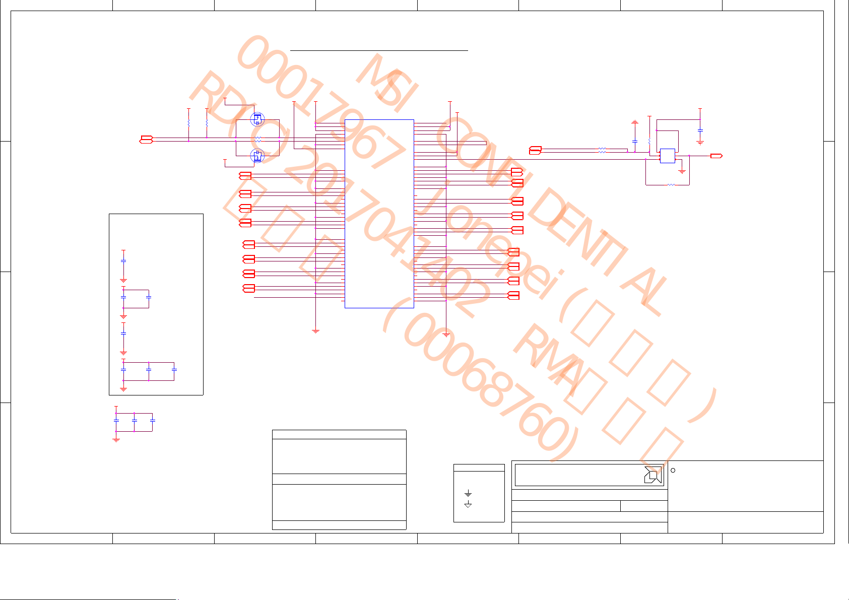
PCI-EXPRES S EDGE CONNECTOR
+3.3V_BUS +3.3V_BUS
SMBCLK
6
IN
SMBDATA
6
BI
C
C
C
Place these c aps as c lose to the P CIE
CAP CER 10UF 20% 16V X5R
connector as poss ible
(1206)1.8MM H MAX
+12V_BUS
12
C14
10uF
16V
+12V_BUS
12
C20
0.15uF
16V
+3.3V_BUS
12
C27
10uF
6.3V
+3.3V_BUS
12
C33
0.1uF
6.3V
12
C21
0.15uF
16V
CAP CER 10UF 10% 6.3V X5R
(0805)1.4MM MAX THICK
12
C34
1uF
6.3V
12
C35
0.01uF
10V
+3.3V_BUS
R4 DNI 0R
R3 DNI 0R
+3.3V_BUS
3
OUT
3
OUT
3
OUT
3
OUT
3
OUT
3
OUT
3
OUT
3
OUT
3
3
3
3
3
3
3
3
1
2 3
1 2
1 2
2 3
1
OUT
OUT
OUT
OUT
OUT
OUT
OUT
OUT
2
12
12
R1
R2
45.3K
45.3K
1%
1%
DNI
DNI
+3.3V_BUS
+3.3V_BUS +12V_BUS +12V_BUS
Q2
BSH111
Q1
BSH111
DNI
DNI
PETP0_GFXRP0
PETN0_GFXRN0
PETP1_GFXRP1
PETN1_GFXRN1
PETP2_GFXRP2
PETN2_GFXRN2
PETP3_GFXRP3
PETN3_GFXRN3
PETP4_GFXRP4
PETN4_GFXRN4
PETP5_GFXRP5
PETN5_GFXRN5
PETP6_GFXRP6
PETN6_GFXRN6
PETP7_GFXRP7
PETN7_GFXRN7
PRESENCE
B1
+12V
B2
+12V
B3
+12V
B4
SMCLK
SMDAT
GND
B5
SMCLK
B6
SMDAT
B7
GND
B8
+3.3V
B13
GND
B14
PETp0
B15
PETn0
B16
GND
B18
GND
B19
PETp1
B20
PETn1
B21
GND
B22
GND
B23
PETp2
B24
PETn2
B25
GND
B26
GND
B27
PETp3
B28
PETn3
B29
GND
B32
GND
B33
PETp4
B34
PETn4
B35
GND
B36
GND
B37
PETp5
B38
PETn5
B39
GND
B40
GND
B41
PETp6
B42
PETn6
B43
GND
B44
GND
B45
PETp7
B46
PETn7
B47
GND
B48
PRSNT2_B48
B49
GND
Mechanical Key
GOLDEN FIN GERS
MPCIE
x8 PCIe
PRSNT1_A1
PERST_
REFCLK+
REFCLK-
JTAG3
JTAG4
PERp0
PERn0
PERp1
PERn1
PERp2
PERn2
PERp3
PERn3
PERp4
PERn4
PERp5
PERn5
PERp6
PERn6
PERp7
PERn7
U4
A
B
C
74AUP1G57GM
1 2
+3.3V_BUS
12
C1011
0.1uF
6.3V
5
VCC
4
PERST#_BUF
Y
2
GND
3,8
OUT
+3.3V_BUS
PRESENCE
A1
A2
+12V
A3
+12V
A4
GND
A6
A7
A9
+3.3V
A10
+3.3V
A11
A12
GND
A13
A14
A15
GND
A16
A17
A18
GND
A20
GND
A21
A22
A23
GND
A24
GND
A25
A26
A27
GND
A28
GND
A29
A30
A31
GND
A34
GND
A35
A36
A37
GND
A38
GND
A39
A40
A41
GND
A42
GND
A43
A44
A45
GND
A46
GND
A47
A48
A49
GND
2
JTDIO_LOOP
PERP4
PERN4
PERP5
PERN5
PERP6
PERN6
PERP7
PERN7
PCIE_REFCLKP
PCIE_REFCLKN
PERP0
PERN0
PERP1
PERN1
PERP2
PERN2
PERP3
PERN3
OUT
OUT
IN
IN
IN
IN
IN
IN
IN
IN
IN
IN
IN
IN
IN
IN
IN
IN
+1.8V_LDO_POK
13,9
OUT
VDDC_PWR_GOOD
14
IN
3
3
3
3
3
3
3
3
3
3
3
3
3
3
3
3
3
3
1 2
R23 0R
1 2
R20 DNI 0R
PERST#
+3.3V_BUS
12
C1012
0.1uF
6.3V
12
R1005
10K
3
1
6
R1007 DNI 0R
DD
DD
DD
C
C
C
BB
BB
BB
+12V_BUS
12
12
C43
0.1uF
16V
A
A
A
8
8
8
12
C44
C47
0.1uF
0.1uF
16V
16V
7
7
7
6
6
6
GROUP NAME DESC RIPTION
COMMON
NOPN
DNI
INT
GPU
SUBBOM
2ND SOURC E
ALT
POWER SUB BOM
VDDC
MVDD
095
1V8
DEBUG
INSTALLED IN MAIN BOM
NO PN,WON 'T BE IN BOM
DON'T INSTALL
INTERNAL BOM, W ON'T BE IN PRODUCTION BOM
GPU PN
SUBBOM PN
ALTERNATIVE PN(FORMAT:ALT=ALT(PN1;PN2;. ..)
VDDC SUB BOM
MVDD SUB BOM
0.95V SUB BOM
1.8V SUB BOM
DEBUG SUB BOM
CONFIDENTIAL AND PROPRIETARY TO ADVANCED MICRO DEVICES INC.
CONFIDENTIAL AND PROPRIETARY TO ADVANCED MICRO DEVICES INC.
1.0
1.0
1.0
CONFIDENTIAL AND PROPRIETARY TO ADVANCED MICRO DEVICES INC.
2015
2015
2015
Advanced Micro Devices
Advanced Micro Devices
Advanced Micro Devices
C
C
C
This AMD Board sch ematic and de sign is the exclusi ve property of AMD, and
This AMD Board sch ematic and de sign is the exclusi ve property of AMD, and
This AMD Board sch ematic and de sign is the exclusi ve property of AMD, and
is provided only to entitie s under a non-dis closure agreemen t with AMD
is provided only to entitie s under a non-dis closure agreemen t with AMD
is provided only to entitie s under a non-dis closure agreemen t with AMD
for evaluation purposes. Further dis tribution or dis closure i s strictl y
for evaluation purposes. Further dis tribution or dis closure i s strictl y
for evaluation purposes. Further dis tribution or dis closure i s strictl y
prohibited. Use of this schema tic and des ign for any purpose other than
prohibited. Use of this schema tic and des ign for any purpose other than
prohibited. Use of this schema tic and des ign for any purpose other than
evaluation requires a Board T echnology Li cense Agreeme nt with AMD.
evaluation requires a Board T echnology Li cense Agreeme nt with AMD.
evaluation requires a Board T echnology Li cense Agreeme nt with AMD.
AMD makes no representations or warranties of a ny kind regarding this
AMD makes no representations or warranties of a ny kind regarding this
AMD makes no representations or warranties of a ny kind regarding this
schematic and design, i ncluding , not limit ed to, any implie d warranty
schematic and design, i ncluding , not limit ed to, any implie d warranty
schematic and design, i ncluding , not limit ed to, any implie d warranty
of merchantability or fitnes s for a particu lar purpose, and di sclai ms
of merchantability or fitnes s for a particu lar purpose, and di sclai ms
of merchantability or fitnes s for a particu lar purpose, and di sclai ms
responsibili ty for any consequences resulting f rom use of the
responsibili ty for any consequences resulting f rom use of the
responsibili ty for any consequences resulting f rom use of the
information incl uded herein.
information incl uded herein.
information incl uded herein.
TITLE:
TITLE:
TITLE:
2
2
2
BANKS DT
BANKS DT
BANKS DT
A
A
A
1
1
1
SYMBOL LEGEND
ACTIVE
LOW
DIGITAL
GROUND
ANALOG
GROUND
BUO#BRING UP
ONLY
LED GREEN "ON" shows PX_EN
5
5
5
4
4
4
AMD - PLATFORM HARDWARE ENG
AMD - PLATFORM HARDWARE ENG
AMD - PLATFORM HARDWARE ENG
#48, No.1387, ZHANGDONG ROAD
#48, No.1387, ZHANGDONG ROAD
#48, No.1387, ZHANGDONG ROAD
SHANGHAI, CHINA 201203
SHANGHAI, CHINA 201203
SHANGHAI, CHINA 201203
PCI-E Edge Connector
PCI-E Edge Connector
PCI-E Edge Connector
SHEET:
SHEET:
SHEET:
Thu Feb 04 02:22:45 2016
Thu Feb 04 02:22:45 2016
Thu Feb 04 02:22:45 2016
DATE:
DATE:
DATE:
2 17
2 17
SHEET NUMBER:
SHEET NUMBER:
SHEET NUMBER:
DOCUMENT NUMBER:
DOCUMENT NUMBER:
DOCUMENT NUMBER:
2 17
105_D0340 0_00A
105_D0340 0_00A
105_D0340 0_00A
3
3
3
OF
OF
OF
REV:
REV:
REV:
Page 3
8
MSI CONFIDENTIAL
00017967 jonepei(裴亮樂)
RD(C)2017041402 RMA工程課
石阿鋒 (00068760)
8
8
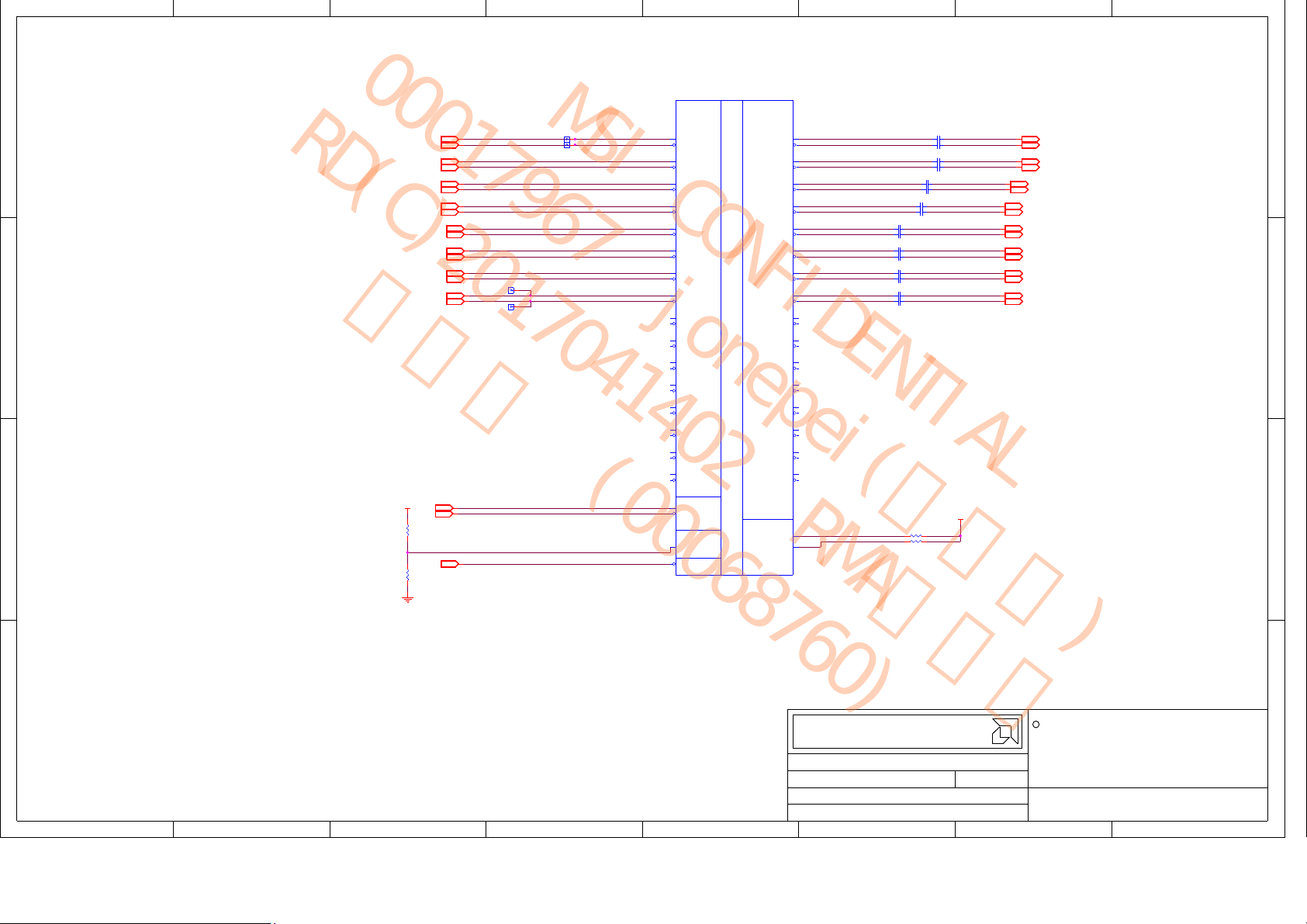
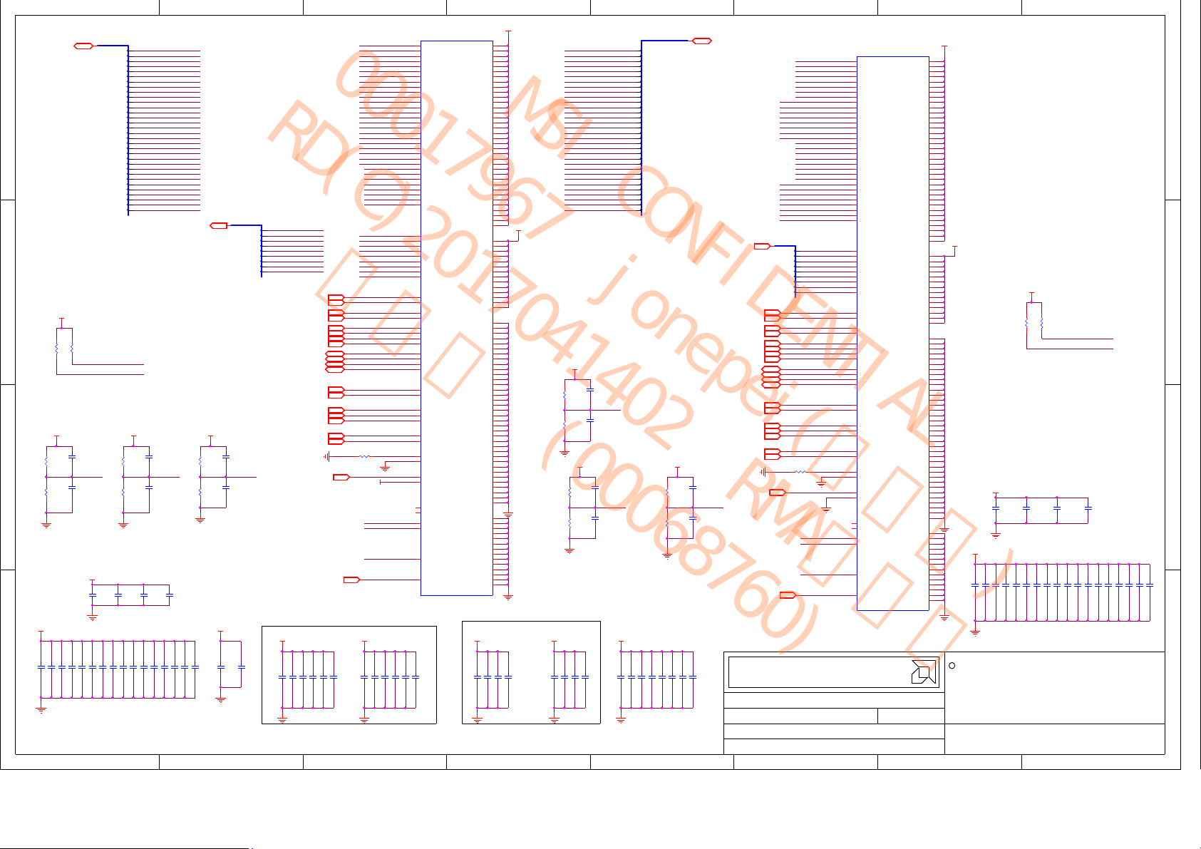
PCIe Interface
7
7
7
6
6
6
345
345
345
2
2
2
1
1
1
2
IN
+1.8V
12
R59
1K
DNI
PWRGOOD_GPU
12
R60
1K
2
IN
2
IN
2
IN
2
IN
2
IN
2
IN
2
IN
2
IN
2
IN
2
IN
2
IN
2
IN
2
IN
2
IN
2
IN
2
IN
2
IN
2,8
IN
C
C
C
TP103
TP104
NOTE: Som e of the PCIE testpoin ts will
be avai lable through vi as on traces.
TP101
TP102
PETP1_GFXRP1
PETN1_GFXRN1
PETP2_GFXRP2
PETN2_GFXRN2
PETP4_GFXRP4
PETN4_GFXRN4
PETP5_GFXRP5
PETN5_GFXRN5
PETP6_GFXRP6
PETN6_GFXRN6
PETP7_GFXRP7
PETN7_GFXRN7
PCIE_REFCLKP
PCIE_REFCLKN
PETP0_GFXRP0
PETN0_GFXRN0
PETP3_GFXRP3
PETN3_GFXRN3
PERST#_BUF
U1A
DD
DD
DD
PCIE_TX3P
PCIE_TX3N
PCIE_TX4P
PCIE_TX4N
PCIE_TX5P
PCIE_TX5N
PCIE_TX6P
PCIE_TX6N
PCIE_TX7P
PCIE_TX7N
PCIE_TX0P
PCIE_TX0N
PCIE_TX1P
PCIE_TX1N
PCIE_TX2P
PCIE_TX2N
PCIE_CALR_TX
PCIE_CALR_RX
C1109 0.22uF 10V
C1110 0.22uF 10V
C1111 0.22uF 10V
C1112 0.22uF 10V
C1113 0.22uF 10V
C1114 0.22uF 10V
C1115 0.22uF 10V
C1116 0.22uF 10V
AF30
PCIE_RX0P
AE31
PCIE_RX0N
AE29
PCIE_RX1P
AD28
PCIE_RX1N
AD30
PCIE_RX2P
AC31
PCIE_RX2N
AC29
PCIE_RX3P
AB28
PCIE_RX3N
AB30
PCIE_RX4P
AA31
PCIE_RX4N
AA29
PCIE_RX5P
Y28
PCIE_RX5N
Y30
PCIE_RX6P
W31
PCIE_RX6N
W29
PCIE_RX7P
V28
PCIE_RX7N
V30
NC#V30
U31
NC#U31
U29
NC#U29
T28
NC#T28
T30
NC#T30
R31
NC#R31
R29
NC#R29
P28
NC#P28
P30
NC#P30
N31
NC#N31
N29
NC#N29
M28
NC#M28
M30
NC#M30
L31
NC#L31
L29
NC#L29
K30
NC#K30
AK30
PCIE_REFCLKP
AK32
PCIE_REFCLKN
N10
TEST_PG
AL27
PERSTB
PCI EXPRESS INTERFACE
CLOCK
CALIBRATION
TOPAZ S3
PCIE_TX0P
PCIE_TX0N
PCIE_TX1P
PCIE_TX1N
PCIE_TX2P
PCIE_TX2N
PCIE_TX3P
PCIE_TX3N
PCIE_TX4P
PCIE_TX4N
PCIE_TX5P
PCIE_TX5N
PCIE_TX6P
PCIE_TX6N
PCIE_TX7P
PCIE_TX7N
NC#W24
NC#W23
NC#V27
NC#U26
NC#U24
NC#U23
NC#T26
NC#T27
NC#T24
NC#T23
NC#P27
NC#P26
NC#P24
NC#P23
NC#M27
NC#N26
PCIE_CALR_TX
PCIE_CALR_RX
AH30
AG31
AG29
AF28
AF27
AF26
AD27
AD26
AC25
AB25
Y23
Y24
AB27
AB26
Y27
Y26
W24
W23
V27
U26
U24
U23
T26
T27
T24
T23
P27
P26
P24
P23
M27
N26
Y22
AA22
1 2
C1 0.22uF 10V
1 2
C31 0.22uF 10V
1 2
C2 0.22uF 10V
1 2
C32 0.22uF 10V
1 2
C3 0.22uF 10V
1 2
C36 0.22uF 10V
1 2
C4 0.22uF 10V
1 2
C13 0.22uF 10V
1 2
1 2
1 2
1 2
1 2
1 2
1 2
1 2
1 2
R8 1.69K 1%
1 2
R10 1K 1%
PERP0
PERN0
PERP1
PERN1
PERP2
PERN2
PERP3
PERN3
PERP4
PERN4
PERP5
PERN5
PERP6
PERN6
PERP7
PERN7
+0.95V
2
OUT
2
OUT
2
OUT
2
OUT
2
OUT
2
OUT
2
OUT
2
OUT
2
OUT
2
OUT
2
OUT
2
OUT
2
OUT
2
OUT
2
OUT
2
OUT
C
C
C
BB
BB
BB
CONFIDENTIAL AND PROPRIETARY TO ADVANCED MICRO DEVICES INC.
CONFIDENTIAL AND PROPRIETARY TO ADVANCED MICRO DEVICES INC.
1.0
1.0
1.0
CONFIDENTIAL AND PROPRIETARY TO ADVANCED MICRO DEVICES INC.
2015
2015
2015
Advanced Micro Devices
Advanced Micro Devices
Advanced Micro Devices
C
C
C
This AMD Board sch ematic and de sign is the exclusi ve property of AMD, and
This AMD Board sch ematic and de sign is the exclusi ve property of AMD, and
This AMD Board sch ematic and de sign is the exclusi ve property of AMD, and
is provided only to entitie s under a non-dis closure agreemen t with AMD
is provided only to entitie s under a non-dis closure agreemen t with AMD
is provided only to entitie s under a non-dis closure agreemen t with AMD
for evaluation purposes. Further dis tribution or dis closure i s strictl y
for evaluation purposes. Further dis tribution or dis closure i s strictl y
for evaluation purposes. Further dis tribution or dis closure i s strictl y
prohibited. Use of this schema tic and des ign for any purpose other than
prohibited. Use of this schema tic and des ign for any purpose other than
prohibited. Use of this schema tic and des ign for any purpose other than
evaluation requires a Board T echnology Li cense Agreeme nt with AMD.
evaluation requires a Board T echnology Li cense Agreeme nt with AMD.
evaluation requires a Board T echnology Li cense Agreeme nt with AMD.
AMD makes no representations or warranties of a ny kind regarding this
AMD makes no representations or warranties of a ny kind regarding this
AMD makes no representations or warranties of a ny kind regarding this
schematic and design, i ncluding , not limit ed to, any implie d warranty
schematic and design, i ncluding , not limit ed to, any implie d warranty
schematic and design, i ncluding , not limit ed to, any implie d warranty
of merchantability or fitnes s for a particu lar purpose, and di sclai ms
of merchantability or fitnes s for a particu lar purpose, and di sclai ms
of merchantability or fitnes s for a particu lar purpose, and di sclai ms
responsibili ty for any consequences resulting f rom use of the
responsibili ty for any consequences resulting f rom use of the
responsibili ty for any consequences resulting f rom use of the
information incl uded herein.
information incl uded herein.
information incl uded herein.
TITLE:
TITLE:
TITLE:
2
2
2
BANKS DT
BANKS DT
BANKS DT
1
1
1
A
A
A
8
8
8
7
7
7
6
6
6
5
5
5
4
4
4
AMD - PLATFORM HARDWARE ENG
AMD - PLATFORM HARDWARE ENG
AMD - PLATFORM HARDWARE ENG
#48, No.1387, ZHANGDONG ROAD
#48, No.1387, ZHANGDONG ROAD
#48, No.1387, ZHANGDONG ROAD
SHANGHAI, CHINA 201203
SHANGHAI, CHINA 201203
SHANGHAI, CHINA 201203
PCIEx8 Interface
PCIEx8 Interface
PCIEx8 Interface
SHEET:
SHEET:
SHEET:
Thu Feb 04 02:22:46 2016
Thu Feb 04 02:22:46 2016
Thu Feb 04 02:22:46 2016
DATE:
DATE:
DATE:
3 17
3 17
SHEET NUMBER:
SHEET NUMBER:
SHEET NUMBER:
DOCUMENT NUMBER:
DOCUMENT NUMBER:
DOCUMENT NUMBER:
3 17
105_D0340 0_00A
105_D0340 0_00A
105_D0340 0_00A
3
3
3
OF
OF
OF
REV:
REV:
REV:
A
A
A
Page 4
8
MSI CONFIDENTIAL
00017967 jonepei(裴亮樂)
RD(C)2017041402 RMA工程課
石阿鋒 (00068760)
8
8
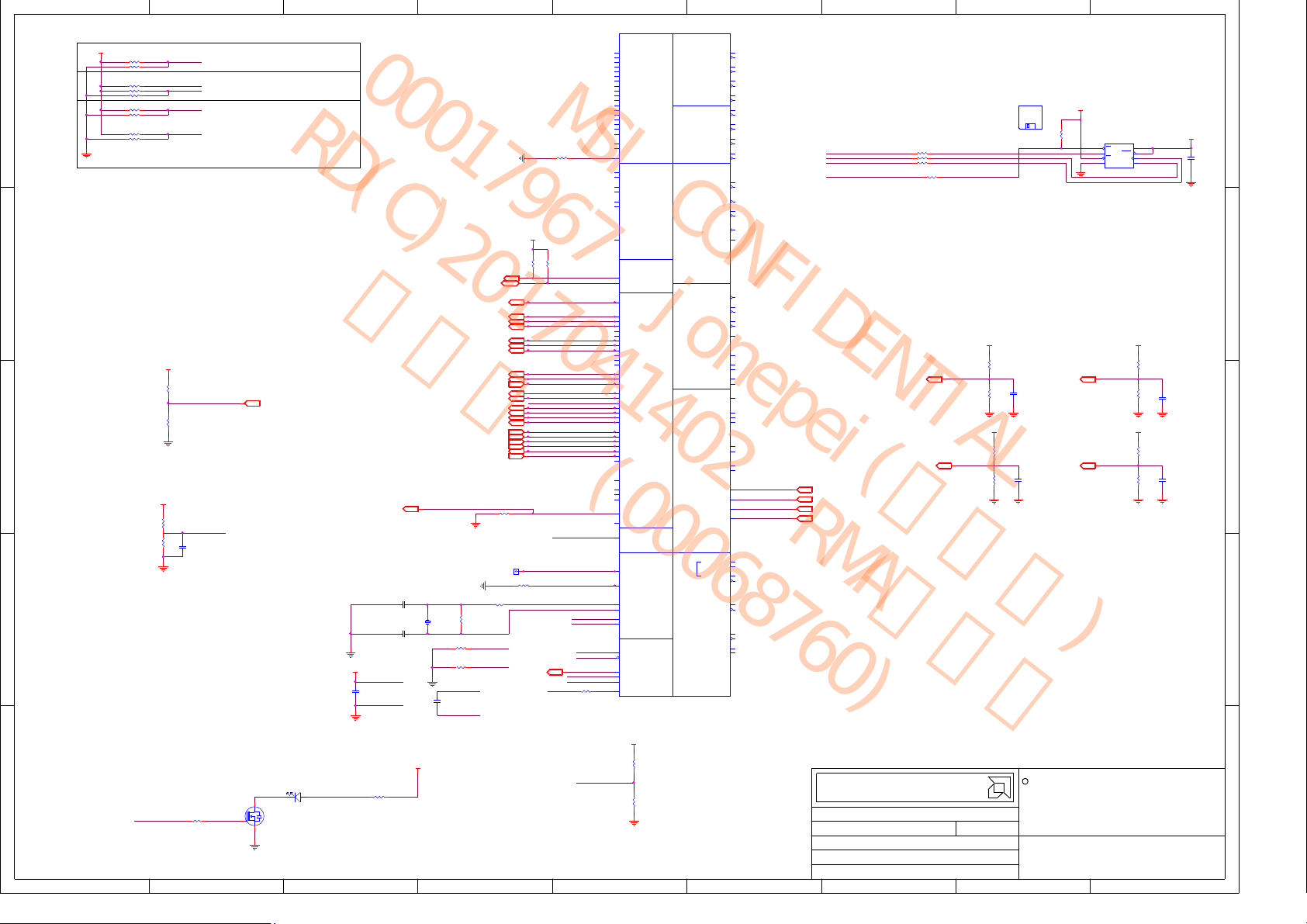
MEM Interface Ch A
7
7
7
6
6
6
345
345
345
2
2
2
1
1
1
C
C
C
MVREFDA/SA =0.7* VDDR1 (GDDR3/4/5)
+MVDD
12
R291
40.2R
1%
DNI
MVREFD_A
MVREFS_A
R2008
DRAM_RST_M
4
4
1 2
Close to MEMORY
MEM Sub BOM
12
12
C295
R292
1uF
100R
6.3V
1%
DNI
DNI
+MVDD
12
DNI
R2006
40.2R
1%
1%
12
DNI
12
C2004
DNI
1uF
6.3V
100R
1%
1%
5
OUT
R3603 1%120R
1 2
MEM 1%49.9R
R3616
R3615 MEM 1%10R
12
C3608
120pF
50V
MEM
1 2
5.1K
R3600
MEM
5,4
1 2
DQA0[31..0]
BI
DQA1[31..0]
5,4
BI
12
C3600
68pF
50V
DNI
DQA00
4 5
0
DQA01
4 5
1
DQA02
4 5
2
DQA03
4 5
3
DQA04
4 5
4
DQA05
4 5
5
DQA06
4 5
6
DQA07
4 5
7
DQA08
4 5
8
DQA09
4 5
9
DQA010
4 5
10
DQA011
4 5
11
DQA012
4 5
12
DQA013
4 5
13
DQA014
4 5
14
DQA015
4 5
15
DQA016
4 5
16
DQA017
4 5
17
DQA018
4 5
18
DQA019
4 5
19
DQA020
4 5
20
DQA021
4 5
21
DQA022
4 5
22
DQA023
4 5
23
DQA024
4 5
24
DQA025
4 5
25
DQA026
4 5
26
DQA027
4 5
27
DQA028
4 5
28
DQA029
4 5
29
DQA030
4 5
30
DQA031
4 5
31
DQA10
4 5
0
DQA11
4 5
1
DQA12
4 5
2
DQA13
4 5
3
DQA14
4 5
4
DQA15
4 5
5
DQA16
4 5
6
DQA17
4 5
7
DQA18
4 5
8
DQA19
4 5
9
DQA110
4 5
10
DQA111
4 5
11
DQA112
4 5
12
DQA113
4 5
13
DQA114
4 5
14
DQA115
4 5
15
DQA116
4 5
16
DQA117
4 5
17
DQA118
4 5
18
DQA119
4 5
19
DQA120
4 5
20
DQA121
4 5
21
DQA122
4 5
22
DQA123
4 5
23
DQA124
4 5
24
DQA125
4 5
25
DQA126
4 5
26
DQA127
4 5
27
DQA128
4 5
28
DQA129
4 5
29
DQA130
4 5
30
DQA131
4 5
31
4
4
DRSTDRST_R
MVREFD_A
MVREFS_A
MEM_CALRP0
CLKTESTA
CLKTESTB
K27
DQA0_0
J29
DQA0_1
H30
DQA0_2
H32
DQA0_3
G29
DQA0_4
F28
DQA0_5
F32
DQA0_6
F30
DQA0_7
C30
DQA0_8
F27
DQA0_9
A28
DQA0_10
C28
DQA0_11
E27
DQA0_12
G26
DQA0_13
D26
DQA0_14
F25
DQA0_15
A25
DQA0_16
C25
DQA0_17
E25
DQA0_18
D24
DQA0_19
E23
DQA0_20
F23
DQA0_21
D22
DQA0_22
F21
DQA0_23
E21
DQA0_24
D20
DQA0_25
F19
DQA0_26
A19
DQA0_27
D18
DQA0_28
F17
DQA0_29
A17
DQA0_30
C17
DQA0_31
E17
DQA1_0
D16
DQA1_1
F15
DQA1_2
A15
DQA1_3
D14
DQA1_4
F13
DQA1_5
A13
DQA1_6
C13
DQA1_7
E11
DQA1_8
A11
DQA1_9
C11
DQA1_10
F11
DQA1_11
A9
DQA1_12
C9
DQA1_13
F9
DQA1_14
D8
DQA1_15
E7
DQA1_16
A7
DQA1_17
C7
DQA1_18
F7
DQA1_19
A5
DQA1_20
E5
DQA1_21
C3
DQA1_22
E1
DQA1_23
G7
DQA1_24
G6
DQA1_25
G1
DQA1_26
G3
DQA1_27
J6
DQA1_28
J1
DQA1_29
J3
DQA1_30
J5
DQA1_31
K26
MVREFDA
J26
MVREFSA
J25
NC#J25
K25
MEM_CALRP0
L10
DRAM_RST
K8
CLKTESTA
L7
CLKTESTB
U1C
GDDR5/DDR3 GDDR5/DDR3
WCKA0_0/DQMA0_0
WCKA0B_0/DQMA0_1
WCKA0_1/DQMA0_2
MEMORY INTERFACE
WCKA0B_1/DQMA0_3
WCKA1_0/DQMA1_0
WCKA1B_0/DQMA1_1
WCKA1_1/DQMA1_2
WCKA1B_1/DQMA1_3
DDBIA0_0/QSA0_0B
DDBIA0_1/QSA0_1B
DDBIA0_2/QSA0_2B
DDBIA0_3/QSA0_3B
DDBIA1_0/QSA1_0B
DDBIA1_1/QSA1_1B
DDBIA1_2/QSA1_2B
DDBIA1_3/QSA1_3B
TOPAZ S3
MAA0_0/MAA_0
MAA0_1/MAA_1
MAA0_2/MAA_2
MAA0_3/MAA_3
MAA0_4/MAA_4
MAA0_5/MAA_5
MAA0_6/MAA_6
MAA0_7/MAA_7
MAA0_8/MAA_13
MAA0_9/MAA_15
MAA1_0/MAA_8
MAA1_1/MAA_9
MAA1_2/MAA_10
MAA1_3/MAA_11
MAA1_4/MAA_12
MAA1_5/MAA_BA2
MAA1_6/MAA_BA0
MAA1_7/MAA_BA1
MAA1_8/MAA_14
MAA1_9/RSVD
EDCA0_0/QSA0_0
EDCA0_1/QSA0_1
EDCA0_2/QSA0_2
EDCA0_3/QSA0_3
EDCA1_0/QSA1_0
EDCA1_1/QSA1_1
EDCA1_2/QSA1_2
EDCA1_3/QSA1_3
ADBIA0/ODTA0
ADBIA1/ODTA1
CLKA0B
CLKA1B
RASA0B
RASA1B
CASA0B
CASA1B
CSA0B_0
CSA0B_1
CSA1B_0
CSA1B_1
K17
J20
H23
G23
G24
H24
J19
K19
G20
L17
J14
K14
J11
J13
H11
G11
J16
L15
G14
L16
E32
E30
A21
C21
E13
D12
E3
F4
H28
C27
A23
E19
E15
D10
D6
G5
H27
A27
C23
C19
C15
E9
C5
H4
L18
K16
H26
CLKA0
H25
G9
CLKA1
H9
G22
G17
G19
G16
H22
J22
G13
K13
K20
CKEA0
J17
CKEA1
G25
WEA0B
H10
WEA1B
4 5
4 5
4 5
4 5
4 5
4 5
4 5
4 5
4 5
4 5
4 5
4 5
4 5
4 5
4 5
4 5
4 5
4 5
MAA00
MAA01
MAA02
MAA03
MAA04
MAA05
MAA06
MAA07
MAA08
MAA10
MAA11
MAA12
MAA13
MAA14
MAA15
MAA16
MAA17
MAA18
WCKA0_0
WCKA0#_0
WCKA0_1
WCKA0#_1
WCKA1_0
WCKA1#_0
WCKA1_1
WCKA1#_1
EDCA0_0
EDCA0_1
EDCA0_2
EDCA0_3
EDCA1_0
EDCA1_1
EDCA1_2
EDCA1_3
DDBIA0_0
DDBIA0_1
DDBIA0_2
DDBIA0_3
DDBIA1_0
DDBIA1_1
DDBIA1_2
DDBIA1_3
ADBIA0
ADBIA1
CLKA0
CLKA#0
CLKA1
CLKA#1
RASA#0
RASA#1
CASA#0
CASA#1
CSA0#_0
CSA1#_0
CKEA0
CKEA1
WEA#0
WEA#1
MAA0[8..0]
0
1
2
3
4
5
6
7
8
MAA1[8..0]
0
1
2
3
4
5
6
7
8
5
OUT
5
OUT
5
OUT
5
OUT
5
OUT
5
OUT
5
OUT
5
OUT
5
OUT
5
OUT
5
OUT
5
OUT
5
OUT
5
OUT
5
OUT
5
OUT
5
BI
5
BI
5
BI
5
BI
5
BI
5
BI
5
BI
5
BI
5
OUT
5
OUT
5
OUT
5
OUT
5
OUT
5
OUT
5
OUT
5
OUT
5
OUT
5
OUT
5
OUT
5
OUT
5
OUT
5
OUT
5
OUT
5
OUT
5,4
OUT
U1F
NC_TXOUT_L3P
NC_TXOUT_L3N
NC_TXOUT_U3P
NC_TXOUT_U3N
AL15
AK14
AH16
AJ15
AL17
AK16
AH18
AJ17
AL19
AK18
AH20
AJ19
AL21
AK20
AH22
AJ21
AL23
AK22
AK24
AJ23
NC_UPHY AB_TMDPA_TX0N
4,5
OUT
NC_UPHY AB_TMDPA_TX0P
NC_UPHY AB_TMDPA_TX1N
NC_UPHY AB_TMDPA_TX1P
NC_UPHY AB_TMDPA_TX2N
NC_UPHY AB_TMDPA_TX2P
NC_UPHY AB_TMDPA_TX3N
NC_UPHY AB_TMDPA_TX3P
NC_TMDP
NC_UPHY AB_TMDPB_TX0N
NC_UPHY AB_TMDPB_TX0P
NC_UPHY AB_TMDPB_TX1N
NC_UPHY AB_TMDPB_TX1P
NC_UPHY AB_TMDPB_TX2N
NC_UPHY AB_TMDPB_TX2P
NC_UPHY AB_TMDPB_TX3N
NC_UPHY AB_TMDPB_TX3P
TOPAZ S3
DD
DD
DD
C
C
C
BB
BB
BB
route 50ohms
single-ended/100ohms diff
and keep short
Match length of CLKTESTA and CLKTESTB
1 2
12
R4027
51.1R
1%
C45
0.1uF
10V
$CDS_IMAGE|clipboard_0.jpg| 146|153
6
6
6
CONFIDENTIAL AND PROPRIETARY TO ADVANCED MICRO DEVICES INC.
CONFIDENTIAL AND PROPRIETARY TO ADVANCED MICRO DEVICES INC.
1.0
1.0
1.0
CONFIDENTIAL AND PROPRIETARY TO ADVANCED MICRO DEVICES INC.
2015
2015
2015
Advanced Micro Devices
Advanced Micro Devices
Advanced Micro Devices
C
C
C
This AMD Board sch ematic and de sign is the exclusi ve property of AMD, and
This AMD Board sch ematic and de sign is the exclusi ve property of AMD, and
This AMD Board sch ematic and de sign is the exclusi ve property of AMD, and
is provided only to entitie s under a non-dis closure agreemen t with AMD
is provided only to entitie s under a non-dis closure agreemen t with AMD
is provided only to entitie s under a non-dis closure agreemen t with AMD
for evaluation purposes. Further dis tribution or dis closure i s strictl y
for evaluation purposes. Further dis tribution or dis closure i s strictl y
for evaluation purposes. Further dis tribution or dis closure i s strictl y
prohibited. Use of this schema tic and des ign for any purpose other than
prohibited. Use of this schema tic and des ign for any purpose other than
prohibited. Use of this schema tic and des ign for any purpose other than
evaluation requires a Board T echnology Li cense Agreeme nt with AMD.
evaluation requires a Board T echnology Li cense Agreeme nt with AMD.
evaluation requires a Board T echnology Li cense Agreeme nt with AMD.
AMD makes no representations or warranties of a ny kind regarding this
AMD makes no representations or warranties of a ny kind regarding this
AMD makes no representations or warranties of a ny kind regarding this
schematic and design, i ncluding , not limit ed to, any implie d warranty
schematic and design, i ncluding , not limit ed to, any implie d warranty
schematic and design, i ncluding , not limit ed to, any implie d warranty
of merchantability or fitnes s for a particu lar purpose, and di sclai ms
of merchantability or fitnes s for a particu lar purpose, and di sclai ms
of merchantability or fitnes s for a particu lar purpose, and di sclai ms
responsibili ty for any consequences resulting f rom use of the
responsibili ty for any consequences resulting f rom use of the
responsibili ty for any consequences resulting f rom use of the
information incl uded herein.
information incl uded herein.
information incl uded herein.
TITLE:
TITLE:
TITLE:
2
2
2
BANKS DT
BANKS DT
BANKS DT
1
1
1
AMD - PLATFORM HARDWARE ENG
AMD - PLATFORM HARDWARE ENG
AMD - PLATFORM HARDWARE ENG
#48, No.1387, ZHANGDONG ROAD
#48, No.1387, ZHANGDONG ROAD
#48, No.1387, ZHANGDONG ROAD
SHANGHAI, CHINA 201203
SHANGHAI, CHINA 201203
SHANGHAI, CHINA 201203
MEM Interface
MEM Interface
MEM Interface
SHEET:
SHEET:
SHEET:
Thu Feb 04 02:22:46 2016
Thu Feb 04 02:22:46 2016
Thu Feb 04 02:22:46 2016
DATE:
DATE:
DATE:
SHEET NUMBER:
SHEET NUMBER:
SHEET NUMBER:
DOCUMENT NUMBER:
DOCUMENT NUMBER:
DOCUMENT NUMBER:
5
5
5
4
4
4
4 17
4 17
4 17
OF
OF
OF
105_D0340 0_00A
105_D0340 0_00A
105_D0340 0_00A
3
3
3
REV:
REV:
REV:
A
A
A
C42
0.1uF
10V
1 2
12
R4026
51.1R
A
A
A
8
8
8
7
7
7
1%
Page 5
1.0
MSI CONFIDENTIAL
00017967 jonepei(裴亮樂)
RD(C)2017041402 RMA工程課
石阿鋒 (00068760)
1.0
1.0
VDDQ_B1
VDDQ_B3
VDDQ_B12
VDDQ_B14
VDDQ_D1
VDDQ_D3
VDDQ_D12
VDDQ_D14
VDDQ_E5
VDDQ_E10
VDDQ_F1
VDDQ_F3
VDDQ_F12
VDDQ_F14
VDDQ_G2
VDDQ_G13
VDDQ_H3
VDDQ_H12
VDDQ_K3
VDDQ_K12
VDDQ_L2
VDDQ_L13
VDDQ_M1
VDDQ_M3
VDDQ_M12
VDDQ_M14
VDDQ_N5
VDDQ_N10
VDDQ_P1
VDDQ_P3
VDDQ_P12
VDDQ_P14
VDDQ_T1
VDDQ_T3
VDDQ_T12
VDDQ_T14
VDD_C5
VDD_C10
VDD_D11
VDD_G1
VDD_G4
VDD_G11
VDD_G14
VDD_L1
VDD_L4
VDD_L11
VDD_L14
VDD_P11
VDD_R5
VDD_R10
VSSQ_A1
VSSQ_A3
VSSQ_A12
VSSQ_A14
VSSQ_C1
VSSQ_C3
VSSQ_C4
VSSQ_C11
VSSQ_C12
VSSQ_C14
VSSQ_E1
VSSQ_E3
VSSQ_E12
VSSQ_E14
VSSQ_F5
VSSQ_F10
VSSQ_H2
VSSQ_H13
VSSQ_K2
VSSQ_K13
VSSQ_M5
VSSQ_M10
VSSQ_N1
VSSQ_N3
VSSQ_N12
VSSQ_N14
VSSQ_R1
VSSQ_R3
VSSQ_R4
VSSQ_R11
VSSQ_R12
VSSQ_R14
VSSQ_V1
VSSQ_V3
VSSQ_V12
VSSQ_V14
VSS_B5
VSS_B10
VSS_D10
VSS_G5
VSS_G10
VSS_H1
VSS_H14
VSS_K1
VSS_K14
VSS_L5
VSS_L10
VSS_P10
VSS_T5
VSS_T10
+MVDD
B1
B3
B12
B14
D1
D3
D12
D14
E5
E10
F1
F3
F12
F14
G2
G13
H3
H12
K3
K12
L2
L13
M1
M3
M12
M14
N5
N10
P1
P3
P12
P14
T1
T3
T12
T14
C5
C10
D11
G1
G4
G11
G14
L1
L4
L11
L14
P11
R5
R10
A1
A3
A12
A14
C1
C3
C4
C11
C12
C14
E1
E3
E12
E14
F5
F10
H2
H13
K2
K13
M5
M10
N1
N3
N12
N14
R1
R3
R4
R11
R12
R14
V1
V3
V12
V14
B5
B10
D10
G5
G10
H1
H14
K1
K14
L5
L10
P10
T5
T10
2
2
2
+MVDD
MEM
60.4R
+MVDD
12
C463
0.1uF
10V
MEM
+MVDD
C325
C326
C327
C328
6.3V
6.3V
6.3V
6.3V
1 2
1 2
1 2
1 2
1 2
1uF
1uF
1uF
1uF
MEM
MEM
DNI
DNI
CONFIDENTIAL AND PROPRIETARY TO ADVANCED MICRO DEVICES INC.
CONFIDENTIAL AND PROPRIETARY TO ADVANCED MICRO DEVICES INC.
CONFIDENTIAL AND PROPRIETARY TO ADVANCED MICRO DEVICES INC.
2015
2015
2015
Advanced Micro Devices
Advanced Micro Devices
Advanced Micro Devices
C
C
C
This AMD Board sch ematic and de sign is the exclusi ve property of AMD, and
This AMD Board sch ematic and de sign is the exclusi ve property of AMD, and
This AMD Board sch ematic and de sign is the exclusi ve property of AMD, and
is provided only to entitie s under a non-dis closure agreemen t with AMD
is provided only to entitie s under a non-dis closure agreemen t with AMD
is provided only to entitie s under a non-dis closure agreemen t with AMD
for evaluation purposes. Further dis tribution or dis closure i s strictl y
for evaluation purposes. Further dis tribution or dis closure i s strictl y
for evaluation purposes. Further dis tribution or dis closure i s strictl y
prohibited. Use of this schema tic and des ign for any purpose other than
prohibited. Use of this schema tic and des ign for any purpose other than
prohibited. Use of this schema tic and des ign for any purpose other than
evaluation requires a Board T echnology Li cense Agreeme nt with AMD.
evaluation requires a Board T echnology Li cense Agreeme nt with AMD.
evaluation requires a Board T echnology Li cense Agreeme nt with AMD.
AMD makes no representations or warranties of a ny kind regarding this
AMD makes no representations or warranties of a ny kind regarding this
AMD makes no representations or warranties of a ny kind regarding this
schematic and design, i ncluding , not limit ed to, any implie d warranty
schematic and design, i ncluding , not limit ed to, any implie d warranty
schematic and design, i ncluding , not limit ed to, any implie d warranty
of merchantability or fitnes s for a particu lar purpose, and di sclai ms
of merchantability or fitnes s for a particu lar purpose, and di sclai ms
of merchantability or fitnes s for a particu lar purpose, and di sclai ms
responsibili ty for any consequences resulting f rom use of the
responsibili ty for any consequences resulting f rom use of the
responsibili ty for any consequences resulting f rom use of the
information incl uded herein.
information incl uded herein.
information incl uded herein.
TITLE:
TITLE:
TITLE:
2
2
2
1
1
1
DD
DD
DD
+MVDD
MEM
1%
1%
R2105
R2106
60.4R
1 2
1 2
CLKA#1
CLKA1
12
12
C488
C448
0.1uF
0.1uF
10V
10V
MEM
MEM
C329
C330
C331
C332
C333
6.3V
1uF
DNI
6.3V
1 2
1uF
DNI
6.3V
1 2
1 2
1uF
DNI
BANKS DT
BANKS DT
BANKS DT
C334
6.3V
6.3V
1 2
1 2
1uF
1uF
DNI
DNI
6.3V
1 2
1uF
DNI
5 4
4
5
12
C489
0.1uF
10V
MEM
C335
C336
C337
C338
C339
6.3V
6.3V
6.3V
6.3V
6.3V
1 2
1 2
1 2
1 2
1uF
MEM
1 2
1uF
1uF
1uF
1uF
MEM
DNI
DNI
DNI
1
1
1
C
C
C
BB
BB
BB
C340
C341
C342
10V
6.3V
6.3V
1 2
1 2
1uF
1uF
0.1uF
MEM
DNI
DNI
A
A
A
5 4
5 4
5 4
5 4
5 4
5 4
5 4
5 4
5 4
5 4
5 4
5 4
5 4
5 4
5 4
5 4
5 4
5 4
5 4
5 4
5 4
5 4
5 4
5 4
5 4
5 4
5 4
5 4
5 4
5 4
5 4
5 4
MAA1[8..0]
IN
IN
IN
IN
EDCA1_2
IN
IN
EDCA1_1
IN
IN
BI
BI
BI
BI
IN
IN
IN
IN
IN
IN
IN
R2114
1 2
DRAM_RST_M
4,5
IN
5
5
5
4
IN
Thu Feb 04 02:22:46 2016
Thu Feb 04 02:22:46 2016
Thu Feb 04 02:22:46 2016
5 17
5 17
5 17
345
345
345
DQA122
DQA123
DQA121
DQA120
DQA116
DQA117
DQA118
DQA119
DQA125
DQA124
DQA127
DQA126
DQA131
DQA129
DQA128
DQA130
DQA115
DQA114
DQA113
DQA112
DQA111
DQA19
DQA18
DQA110
DQA11
DQA10
DQA12
DQA13
DQA15
DQA17
DQA14
DQA16
5 4
8
5 4
7
5 4
6
5 4
5
5 4
4
5 4
3
5 4
2
5 4
1
5 4
0
WCKA1_0
WCKA1#_0
WCKA1_1
WCKA1#_1
EDCA1_3
EDCA1_0
DDBIA1_2
DDBIA1_3
DDBIA1_1
DDBIA1_0
RASA#1
CASA#1
CKEA1
CLKA#1
CLKA1
CSA1#_0
WEA#1
MEM
VREFD1_A1
VREFD2_A1
VREFC_A1
ADBIA1
105_D0340 0_00A
105_D0340 0_00A
105_D0340 0_00A
3
3
3
MEM
U2104
M2
DQ31__DQ7
M4
DQ30__DQ6
N2
DQ29__DQ5
N4
DQ28__DQ4
T2
DQ27__DQ3
T4
DQ26__DQ2
V2
DQ25__DQ1
V4
DQ24__DQ0
M13
DQ23__DQ15
M11
DQ22__DQ14
N13
DQ21__DQ13
N11
DQ20__DQ12
T13
DQ19__DQ11
T11
DQ18__DQ10
V13
DQ17__DQ9
V11
DQ16__DQ8
F13
DQ15__DQ23
F11
DQ14__DQ22
E13
DQ13__DQ21
E11
DQ12__DQ20
B13
DQ11__DQ19
B11
DQ10__DQ18
A13
DQ9__DQ17
A11
DQ8__DQ16
F2
DQ7__DQ31
F4
DQ6__DQ30
E2
DQ5__DQ29
E4
DQ4__DQ28
B2
DQ3__DQ27
B4
DQ2__DQ26
A2
DQ1__DQ25
A4
DQ0__DQ24
MAA18
J5
RFU_A12_NC
MAA17
K4
A7_A8__A0_A10
MAA16
K5
A6_A11__A1_A9
MAA15
K10
A5_BA1__A3_BA3
MAA14
K11
A4_BA2__A2_BA0
MAA13
H10
A3_BA3__A5_BA1
MAA12
H11
A2_BA0__A4_BA2
MAA11
H5
A1_A9__A6_A11
MAA10
H4
A0_A10__A7_A8
D4
WCK01__WCK23
D5
WCK01#__WCK23#
P4
WCK23__WCK01
P5
WCK23#__WCK01#
R2
EDC3__EDC0
R13
EDC2__EDC1
C13
EDC1__EDC2
C2
EDC0__EDC3
P2
DBI3#__DBI0#
P13
DBI2#__DBI1#
D13
DBI1#__DBI2#
D2
DBI0#__DBI3#
G3
RAS#__CAS#
L3
CAS#__RAS#
J3
CKE#
J11
CK#
J12
CK
G12
CS#__WE#
L12
WE#__CS#
1%120R
ZQ_A1_1
J13
ZQ
J10
SEN
J2
RESET#
J1
MF
A5
Vpp_NC
V5
Vpp_NC1
A10
VREFD1
V10
VREFD2
J14
VREFC
J4
ABI#
GDDR5
GDDR5 CHA&B X32
GDDR5 CHA&B X32
GDDR5 CHA&B X32
REV:
REV:
REV:
OF
OF
OF
5 4
5 4
5 4
5 4
5 4
5 4
5 4
5 4
5 4
5 4
5 4
5 4
5 4
5 4
5 4
5 4
5 4
5 4
5 4
5 4
5 4
5 4
5 4
5 4
5 4
5 4
5 4
5 4
5 4
5 4
5 4
5 4
5 4
5 4
5 4
5 4
5 4
5 4
5 4
5 4
5 4
IN
IN
IN
IN
IN
IN
IN
IN
BI
BI
BI
BI
IN
IN
IN
IN
IN
IN
IN
R2110
IN
4
IN
Overlap 0805 / 0603 footprints.
12
C369DNI
6.3V
10uF
6
6
6
VDDQ_B1
VDDQ_B3
VDDQ_B12
VDDQ_B14
VDDQ_D1
VDDQ_D3
VDDQ_D12
VDDQ_D14
VDDQ_E5
VDDQ_E10
VDDQ_F1
VDDQ_F3
VDDQ_F12
VDDQ_F14
VDDQ_G2
VDDQ_G13
VDDQ_H3
VDDQ_H12
VDDQ_K3
VDDQ_K12
VDDQ_L2
VDDQ_L13
VDDQ_M1
VDDQ_M3
VDDQ_M12
VDDQ_M14
VDDQ_N5
VDDQ_N10
VDDQ_P1
VDDQ_P3
VDDQ_P12
VDDQ_P14
VDDQ_T1
VDDQ_T3
VDDQ_T12
VDDQ_T14
VDD_C10
VDD_D11
VDD_G11
VDD_G14
VDD_P11
VDD_R10
VSSQ_A1
VSSQ_A3
VSSQ_A12
VSSQ_A14
VSSQ_C1
VSSQ_C3
VSSQ_C4
VSSQ_C11
VSSQ_C12
VSSQ_C14
VSSQ_E1
VSSQ_E3
VSSQ_E12
VSSQ_E14
VSSQ_F5
VSSQ_F10
VSSQ_H2
VSSQ_H13
VSSQ_K2
VSSQ_K13
VSSQ_M5
VSSQ_M10
VSSQ_N1
VSSQ_N3
VSSQ_N12
VSSQ_N14
VSSQ_R1
VSSQ_R3
VSSQ_R4
VSSQ_R11
VSSQ_R12
VSSQ_R14
VSSQ_V1
VSSQ_V3
VSSQ_V12
VSSQ_V14
VSS_B10
VSS_D10
VSS_G10
VSS_H14
VSS_K14
VSS_P10
VSS_T10
+MVDD
12
B1
B3
B12
B14
D1
D3
D12
D14
E5
E10
F1
F3
F12
F14
G2
G13
H3
H12
K3
K12
L2
L13
M1
M3
M12
M14
N5
N10
P1
P3
P12
P14
T1
T3
T12
T14
C5
VDD_C5
C10
D11
G1
VDD_G1
G4
VDD_G4
G11
G14
L1
VDD_L1
L4
VDD_L4
L11
VDD_L11
L14
VDD_L14
P11
R5
VDD_R5
R10
A1
A3
A12
A14
C1
C3
C4
C11
C12
C14
E1
E3
E12
E14
F5
F10
H2
H13
K2
K13
M5
M10
N1
N3
N12
N14
R1
R3
R4
R11
R12
R14
V1
V3
V12
V14
B5
VSS_B5
B10
D10
G5
VSS_G5
G10
H1
VSS_H1
H14
K1
VSS_K1
K14
L5
VSS_L5
L10
VSS_L10
P10
T5
VSS_T5
T10
Overlap 0805 / 0603 footprints.
12
12
C378DNI
C379DNI
6.3V
6.3V
10uF
10uF
+MVDD
6.3V
C2109
1uF
6.3V
VREFD2_A1
DQA1[31..0]
0
1
2
3
4
5
6
7
8
9
10
11
12
13
14
15
16
17
18
19
20
21
22
23
24
25
26
27
28
29
30
31
5
12
MEM
R2119
2.37K
1%
5
1%
R2120
5.49K
1 2
+MVDD
12
12
12
12
12
C373MEM
C374MEM
C370MEM
C371MEM
C372MEM
10V
10V
10V
10V
10V
0.1uF
0.1uF
0.1uF
0.1uF
0.1uF
4
4
4
DQA10
5 4
DQA11
5 4
DQA12
5 4
DQA13
5 4
DQA14
5 4
DQA15
5 4
DQA16
5 4
DQA17
5 4
DQA18
5 4
DQA19
5 4
DQA110
5 4
DQA111
5 4
DQA112
5 4
DQA113
5 4
DQA114
5 4
DQA115
5 4
DQA116
5 4
DQA117
5 4
DQA118
5 4
DQA119
5 4
DQA120
5 4
DQA121
5 4
DQA122
5 4
DQA123
5 4
DQA124
5 4
DQA125
5 4
DQA126
5 4
DQA127
5 4
DQA128
5 4
DQA129
5 4
DQA130
5 4
DQA131
5 4
+MVDD
+MVDD
12
DNI
12
C2105
DNI
1uF
R2112
2.37K
1%
VREFD1_A1
DNI
1%
DNI
C2107
R2115
1uF
1 2
5.49K
1 2
6.3V
+MVDD
12
DNI
12
DNI
R2117
2.37K
1%
DNI
1%
DNI
C2110
R2118
1uF
1 2
5.49K
1 2
6.3V
+MVDD
12
12
C380DNI
C381DNI
6.3V
6.3V
10uF
10uF
5
5
5
12
12
12
MC380DNI
MC381DNI
MC378DNI
MC379MEM
6.3V
6.3V
6.3V
6.3V
4.7uF
4.7uF
4.7uF
4.7uF
4,5
BI
4,5
IN
4
4
4
4
4
4
4
4
4
4
4
4
4
4
4
4,5
4,5
4
+MVDD
12
MEM
C2111
1uF
6.3V
VREFC_A1
MEM
MEM
C2112
1uF
1 2
6.3V
12
12
12
C375DNI
C376DNI
C377MEM
10V
10V
10V
0.1uF
0.1uF
0.1uF
4
5
AMD - PLATFORM HARDWARE ENG
AMD - PLATFORM HARDWARE ENG
AMD - PLATFORM HARDWARE ENG
#48, No.1387, ZHANGDONG ROAD
#48, No.1387, ZHANGDONG ROAD
#48, No.1387, ZHANGDONG ROAD
SHANGHAI, CHINA 201203
SHANGHAI, CHINA 201203
SHANGHAI, CHINA 201203
SHEET:
SHEET:
SHEET:
DATE:
DATE:
DATE:
SHEET NUMBER:
SHEET NUMBER:
SHEET NUMBER:
DOCUMENT NUMBER:
DOCUMENT NUMBER:
DOCUMENT NUMBER:
M2
M4
N2
N4
T2
T4
V2
V4
M13
M11
N13
N11
T13
T11
V13
V11
F13
F11
E13
E11
B13
B11
A13
A11
F2
F4
E2
E4
B2
B4
A2
A4
J5
K4
K5
K10
K11
H10
H11
H5
H4
D4
D5
P4
P5
R2
R13
C13
C2
P2
P13
D13
D2
G3
L3
J3
J11
J12
G12
L12
J13
J10
J2
J1
A5
V5
A10
V10
J14
J4
12
MC368MEM
6.3V
4.7uF
DQ31__DQ7
DQ30__DQ6
DQ29__DQ5
DQ28__DQ4
DQ27__DQ3
DQ26__DQ2
DQ25__DQ1
DQ24__DQ0
DQ23__DQ15
DQ22__DQ14
DQ21__DQ13
DQ20__DQ12
DQ19__DQ11
DQ18__DQ10
DQ17__DQ9
DQ16__DQ8
DQ15__DQ23
DQ14__DQ22
DQ13__DQ21
DQ12__DQ20
DQ11__DQ19
DQ10__DQ18
DQ9__DQ17
DQ8__DQ16
DQ7__DQ31
DQ6__DQ30
DQ5__DQ29
DQ4__DQ28
DQ3__DQ27
DQ2__DQ26
DQ1__DQ25
DQ0__DQ24
RFU_A12_NC
A7_A8__A0_A10
A6_A11__A1_A9
A5_BA1__A3_BA3
A4_BA2__A2_BA0
A3_BA3__A5_BA1
A2_BA0__A4_BA2
A1_A9__A6_A11
A0_A10__A7_A8
WCK01__WCK23
WCK01#__WCK23#
WCK23__WCK01
WCK23#__WCK01#
EDC3__EDC0
EDC2__EDC1
EDC1__EDC2
EDC0__EDC3
DBI3#__DBI0#
DBI2#__DBI1#
DBI1#__DBI2#
DBI0#__DBI3#
RAS#__CAS#
CAS#__RAS#
CKE#
CK#
CK
CS#__WE#
WE#__CS#
ZQ
SEN
RESET#
MF
Vpp_NC
Vpp_NC1
VREFD1
VREFD2
VREFC
ABI#
MC369MEM
6.3V
4.7uF
U2102
GDDR5
DQA014
DQA015
DQA013
DQA012
DQA010
DQA08
DQA011
DQA09
DQA01
DQA00
DQA02
DQA03
DQA05
DQA06
DQA04
DQA07
DQA022
DQA023
DQA021
DQA020
DQA017
DQA018
DQA016
DQA025
DQA026
DQA027
DQA029
DQA030
DQA028DQA029
DQA031
MAA08
MAA00
MAA01
MAA03MAA04
MAA02MAA03
MAA05
MAA04
MAA06
MAA07
WCKA0_1
WCKA0#_1
WCKA0_0
WCKA0#_0
EDCA0_1
EDCA0_0
EDCA0_2
EDCA0_3
DDBIA0_1
DDBIA0_0
DDBIA0_2
DDBIA0_3
CASA#0
RASA#0
CKEA0
CLKA#0
CLKA0
WEA#0
CSA0#_0
MEM
1%120R
ZQ_A0_1
1 2
DRAM_RST_M
+MVDD
VREFD1_A0
5
VREFD2_A0
5
5
12
ADBIA0
MC364DNI
6.3V
4.7uF
VREFC_A0
12
6
6
6
12
MC365DNI
MC366DNI
6.3V
6.3V
4.7uF
4.7uF
12
12
MC367DNI
6.3V
4.7uF
MEM
8
8
8
CHANNEL A: 1GB/512MB GDDR5
DQA0[31..0]
4,5
BI
DQA00
0
DQA01
1
DQA02
2
DQA03
3
DQA04
4
DQA05
5
DQA06
6
DQA07
7
DQA08
8
DQA09
9
DQA010
10
DQA011
11
DQA012
12
DQA013
13
DQA014
14
DQA015
15
DQA016
16
DQA017
17
DQA018
18
DQA019 DQA019
19
DQA020
20
DQA021
21
DQA022
22
DQA023
23
DQA024 DQA024
24
DQA025
25
DQA026
26
DQA027
27
DQA028
28
29
DQA030
30
DQA031
31
7
7
7
(5) GDDR5 Memory Channel A&B
5 4
5 4
5 4
5 4
5 4
5 4
5 4
5 4
5 4
5 4
5 4
5 4
5 4
5 4
5 4
5 4
5 4
5 4
5 4
5 4
5 4
5 4
5 4
5 4
5 4
5 4
5 4
5 4
5 4
5 4
5 4
5 4
MAA0[8..0]
4,5
OUT
MAA08
5 4
8
MAA07
5 4
7
MAA06
5 4
6
MAA05
5 4
5
5 4
4
5 4
3
MAA02
5 4
2
MAA01
5 4
1
MAA00
5 4
0
C
C
C
+MVDD
MEM
MEM
1%
1%
R2101
R2102
60.4R
60.4R
1 2
1 2
CLKA#0
CLKA0
+MVDD
12
DNI
12
DNI
+MVDD
A
A
A
1 2
C2101
1uF
R2103
2.37K
6.3V
1%
VREFD1_A0
DNI
1%
R2107
5.49K
1 2
C301MEM
C300DNI
6.3V
6.3V
1 2
1 2
1uF
1uF
5
DNI
C2103
1uF
1 2
6.3V
+MVDD
12
C487
0.1uF
10V
MEM
C302MEM
C303DNI
C304DNI
C305DNI
C306MEM
10V
6.3V
6.3V
6.3V
6.3V
1 2
1 2
1 2
1 2
1uF
1uF
1uF
1uF
0.1uF
8
8
8
5 4
5 4
+MVDD +MVDD
12
DNI
12
C2102
DNI
1uF
R2104
2.37K
6.3V
1%
VREFD2_A0
DNI
1%
DNI
C2104
R2108
1uF
1 2
5.49K
1 2
6.3V
12
12
C413
0.1uF
10V
MEM
C307DNI
6.3V
1 2
1 2
1uF
12
C486
0.1uF
10V
MEM
C309DNI
C310MEM
C311DNI
C308MEM
C312DNI
6.3V
6.3V
6.3V
10V
6.3V
1 2
1 2
1 2
1 2
1uF
1uF
1uF
1uF
0.1uF
12
MEM
12
MEM
C2106
1uF
R2113
2.37K
6.3V
1%
VREFC_A0
5
1%
MEM
R2116
5.49K
1 2
C438
0.1uF
10V
MEM
+MVDD
C313DNI
C314DNI
C315DNI
6.3V
6.3V
6.3V
1 2
1 2
1 2
1uF
1uF
1uF
5
MEM
C2108
1uF
1 2
6.3V
+MVDD +MVDD
12
12
C355
C356
0.1uF
0.1uF
10V
10V
DNI
MEM
7
7
7
4
4
4
4
4
4
4
4
4
4
4
4
4
4
4
4,5
4,5
4
4
4,5
12
12
12
12
12
C364DNI
C365DNI
C366DNI
C367DNI
C368DNI
6.3V
6.3V
6.3V
6.3V
6.3V
10uF
10uF
10uF
10uF
10uF
Page 6
9
MSI CONFIDENTIAL
00017967 jonepei(裴亮樂)
RD(C)2017041402 RMA工程課
石阿鋒 (00068760)
9
9
PIN BASED STRAPS
+3.3V_BUS
R45 DNI 10K
1 2
MR45 DNI 10K
1 2
R53 DNI 10K1 2
R54 DNI 10K1 2
E
E
E
D
D
D
C
C
C
B
B
B
MR54 DNI 10K1 2
R87 DNI 4.7K
1 2
MR87 DNI 4.7K
1 2
R88 DNI 4.7K1 2
MR88 DNI 4.7K1 2
+3.3V_BUS
12
12
+1.8V
12
DNI
R1201
499R
1%
12
R1200
249R
1%
DNI
8
8
8
GPIO(0) - TX_PWRS_ENB (Transmitter Power Savings Enable)
GPIO0
0: 50% Tx output swing for mobile mode
6
1: full Tx output swing (Default setting for Desktop)
CLKREQ#
6
GPIO_9_R
GPIO5
GPIO16
6
6
6
R752
10K
DNI
GPIO_21_MVDDCNTL GPIO_21_MVDDCNTL
MR752
10K
DNI
NC_DBG_VREFG
12
PLACE VREFG DIVIDER AND CAP
C1204
0.1uF
CLOSE TO ASIC
10V
DNI
IN
6
6
7 46 5 123
7 46 5 123
7 46 5 123
U1B
N9
NC_DBG_DATA16
L9
NC_DBG_DATA15
AE9
NC_DBG_DATA14
Y11
NC_DBG_DATA13
AE8
NC_DBG_DATA12
AD9
DBG_DATA11
AC10
DBG_DATA10
AD7
DBG_DATA9
AC8
DBG_DATA8
AC7
DBG_DATA7
AB9
DBG_DATA6
AB8
DBG_DATA5
AB7
DBG_DATA4
AB4
DBG_DATA3
AB2
GPIO0
SMBDATA
SMBCLK
GPIO5
GPIO8
GPIO9
GPIO10
GPIO16
GPIO19_CTF
GPIO22
XO_IN
XO_IN2
GPU_DPLUS
GPU_DMINUS
TS_FDO
TSVDD
TSVSS
R98
DBG_DATA2
Y8
DBG_DATA1
Y7
DBG_DATA0
AL9
NC_DBG_CNTL0
U1
BP_0
U3
BP_1
AM26
DIECRACKMON
W6
NC#W6
V6
NC#V6
AC6
NC#AC5
AC5
NC#AC6
AA5
NC#AA5
AA6
NC#AA6
Y6
NC#Y6
I2C
R1
SCL
R3
SDA
GENERAL PURPOSE I/O
U6
GPIO_0
U8
SMBDAT
U7
SMBCLK
T9
GPIO_5_AC_BATT
T8
GPIO_6_TACH
T7
NC_GPIO_7
P10
GPIO_8_ROMSO
P4
GPIO_9_ROMSI
P2
GPIO_10_ROMSCK
N6
GPIO_11
N5
GPIO_12
N3
GPIO_13
N1
GPIO_15_PWRCNTL_0
M4
GPIO_16
R6
GPIO_17_THERMAL_INT
M2
GPIO_19_CTF
P8
GPIO_20_PWRCNTL_1
P7
GPIO_21
N8
GPIO_22_ROMCSB
AK10
GPIO_29
AM10
GPIO_30
CLKREQ#
N7
CLKREQB
L6
JTAG_TRST B
L5
JTAG_TDI
L3
JTAG_TCK
L1
JTAG_TMS
K4
JTAG_TDO
K7
TESTEN
AF24
NC#AF24
W8
NC_GENERICB
W7
NC_GENERICD
AD10
NC_GENERICE_HPD4
AJ9
NC#AJ9
AB16
PX_EN
AJ27
WAKEB
AC16
NC_DBG_VREFG
PLL/CLOCK
AA1
PLL_ANALOG_IN
AA3
PLL_ANALOG_OUT
AM28
XTALIN
AK28
XTALOUT
AC22
XO_IN
AB22
XO_IN2
THERMAL
T4
DPLUS
T2
DMINUS
R5
GPIO28_FDO
AD17
TSVDD
AC17
TSVSS
0R
12
AE19
TS_A
DNI
DNI
10K
1 2
R311
+3.3V_BUS
R5
R6
4.7K
4.7K
1 2
1 2
9
OUT
9
BI
6
OUT
2
OUT
2
OUT
6
OUT
6
OUT
6
OUT
6
OUT
9
OUT
6
OUT
8
IN
8
OUT
9
OUT
6
OUT
9
OUT
9 GPIO_30_VID3
OUT
6
OUT
11
IN
11
IN
11
IN
11
IN
11
OUT
11
IN
PX_EN
6
OUT
C82 50V12pF1 2
C83
+1.8V
TSVDD
12
C4020
1uF
6.3V
TSVSS
1 2
12
Y1
12pF
50V
6
6
R7 DNI 1K1 2
R30 0R1 2
12
R31
1M
1%
27.000MHz
R34 DNI 5.1K
1 2
R36 DNI 5.1K1 2
GPU_DPLUS
12
DNI
6
C4004
0.0022uF
50V
GPU_DMINUS
6
TP1
R46 1%16. 2K
1 2
XO_IN
6
XO_IN2
6
SCL
SDA
GPIO_15_VID0
GPIO17_THERMAL_INT
GPIO_20_VID1
6
GPIO_29_VID2
JTAG_TRST B
JTAG_TDI
JTAG_TCK
JTAG_TMS
JTAG_TDO
TESTEN
NC_DBG_VREFG
6
PLL_ANALOG_IN
PLL_ANALOG_OUT
XTALIN
XTALOUT
6
6
6
6
8
OUT
6
6
VR_TT_A
6
NC_DPA
DBG
NC_DPB
NC_DPC
NC_DAC1
MLPS&SVI2
NC_DDC/ AUX
TOPAZ S3
NC_AVSSN#AK26
NC_AVSSN#AJ25
NC_AVSSN#AG25
NC_HSYNC
NC_RSET
NC_AVDD
NC_AVSSQ
NC_VDD1DI
NC_VSS1DI
GPIO_SVD
GPIO_SVT
GPIO_SVC
NC_GENLK_CLK
NC_GENLK_VSYNC
NC_SWAPLOCKA
NC_SWAPLOCKB
NC_DDC1CLK
NC_DDC1DATA
NC_AUX1P
NC_AUX1N
NC_AUX2P
NC_AUX2N
NC_DDCVGACLK
NC_DDCVGADATA
AF2
NC#AF2
AF4
NC#AF4
AG3
NC#AG3
AG5
NC#AG5
AH3
NC#AH3
AH1
NC#AH1
AK3
NC#AK3
AK1
NC#AK1
AK5
NC#AK5
AM3
NC#AM3
AK6
NC#AK6
AM5
NC#AM5
AJ7
NC#AJ7
AH6
NC#AH6
AK8
NC#AK8
AL7
NC#AL7
V4
NC#V4
U5
NC#U5
V2
NC#V2
Y4
NC#Y4
W5
NC#W5
Y2
NC#Y2
J8
NC#J8
AK26
AL25
NC_G
AJ25
AH24
NC_B
AG25
AH26
AD22
AG24
AE22
AE23
AD23
AM12
NC_CEC
AK12
AL11
AJ11
AL13
AJ13
AG13
AH12
PS_0
AC19
PS_0
AD19
PS_1
AE17
PS_2
AE20
PS_3
AE6
AE5
AD2
AD4
AD13
AD11
AE16
NC#AE16
AD16
NC#AD16
AC1
AC3
IN
PS_1
IN
PS_2
IN
PS_3
IN
GPIO8
6
GPIO9
6
GPIO10
6
GPIO22
6
6
6
6
6
R13 33R
1 2
R14 33R
1 2
R15 33R
1 2
R16 33R1 2
6
OUT
6
OUT
GPIO_22_ROMCSB_R
PS_0
PS_1
VIDEO BIOS
FIRMWARE
BIOS
+3.3V_BUS
BIOS
12
R24
DNI
2.2K
GPIO_8_R
GPIO_9_R
6
GPIO_10_R
+1.8V
12
R25
3.24K
1%
PS_0 [01101]
DNI
12
12
R26
C24
5.62K
0.082uF
1%
16V
+1.8V
12
R64
8.45K
1%
PS_1 [11001]
DNI
12
12
DNI
R11
C19
2K
0.01uF
1%
25V
$CDS_IMAGE|clipboa rd_1_0_SI6.jpg| 2694| 1465
U2
1
CE
VDD
2
SO
HOLD
3
WP
SCK
4
GND5SI
PM25LD010C-SCE
1Mbit ROM
PS_2
6
OUT
PS_3
6
OUT
+3.3V_BUS
8
7
6
+1.8V
12
R17
4.75K
1%
PS_2 [00000]
DNI
12
12
R18
4.75K
C22
1%
0.68uF
DNI
4V
+1.8V
DNI
12
DNI
R19
4.75K
1%
PS_3 [00000]
DNI
12
12
C23
R27
0.68uF
4.75K
4V
1%
E
E
E
12
C57
0.1uF
6.3V
D
D
D
C
C
C
B
B
B
+3.3V_BUS
12
R585
+3.3V_BUS
A
A
A
PX_EN
R9 INT 1%10K1 2
6
9
9
9
1
D1 INT
1 2
GREEN
LED_PWR
R33 INT 1%499R1 2
7
7
7
PX_EN#
Q3
2N7002E
INT
2 3
6
18.2K
1%
VR_TT_A
DNI
DNI
12
R587
11K
0.5%
58 6 3
58 6 3
58 6 3
4
4
4
AMD - PLATFORM HARDWARE ENG
AMD - PLATFORM HARDWARE ENG
AMD - PLATFORM HARDWARE ENG
#48, No.1387, ZHANGDONG ROAD
#48, No.1387, ZHANGDONG ROAD
#48, No.1387, ZHANGDONG ROAD
SHANGHAI, CHINA 201203
SHANGHAI, CHINA 201203
SHANGHAI, CHINA 201203
SHEET:
SHEET:
SHEET:
DATE:
DATE:
DATE:
SHEET NUMBER:
SHEET NUMBER:
SHEET NUMBER:
DOCUMENT NUMBER:
DOCUMENT NUMBER:
DOCUMENT NUMBER:
NOTES:
NOTES:
NOTES:
Main
Main
Main
Thu Feb 04 02:22 :47 201 6
Thu Feb 04 02:22 :47 201 6
Thu Feb 04 02:22 :47 201 6
NOTE
NOTE
NOTE
6
6
6
OF
OF
OF
105_D034 00_00A
105_D034 00_00A
105_D034 00_00A
CONFIDENTIAL AND PROPRIETARY TO ADVANCED MICRO DEVICES INC.
CONFIDENTIAL AND PROPRIETARY TO ADVANCED MICRO DEVICES INC.
CONFIDENTIAL AND PROPRIETARY TO ADVANCED MICRO DEVICES INC.
2015
2015
2015
C
Advanced Micro Devices
C
Advanced Micro Devices
C
Advanced Micro Devices
This AMD Board schematic and design is the exclusive property of AMD, and
This AMD Board schematic and design is the exclusive property of AMD, and
This AMD Board schematic and design is the exclusive property of AMD, and
is provided only to entities under a non-disclosure agreement with AMD
is provided only to entities under a non-disclosure agreement with AMD
is provided only to entities under a non-disclosure agreement with AMD
for evaluation purposes. Further distribution or disclosure is strictly
for evaluation purposes. Further distribution or disclosure is strictly
for evaluation purposes. Further distribution or disclosure is strictly
prohibited. Use of this schematic and design for any purpose other than
prohibited. Use of this schematic and design for any purpose other than
prohibited. Use of this schematic and design for any purpose other than
evaluation requires a Board Technology License Agreement with AMD.
evaluation requires a Board Technology License Agreement with AMD.
evaluation requires a Board Technology License Agreement with AMD.
AMD makes no representations or warranties of any kind regarding this
AMD makes no representations or warranties of any kind regarding this
AMD makes no representations or warranties of any kind regarding this
schematic and design, including, not limited to, any implied warranty
schematic and design, including, not limited to, any implied warranty
schematic and design, including, not limited to, any implied warranty
of merchantability or fitness for a particular purpose, and disclaims
of merchantability or fitness for a particular purpose, and disclaims
of merchantability or fitness for a particular purpose, and disclaims
responsibility for any consequences resulting from use of the
responsibility for any consequences resulting from use of the
responsibility for any consequences resulting from use of the
1.0
1.0
1.0
REV:
REV:
REV:
17
17
17
information included herein.
information included herein.
information included herein.
TITLE:
TITLE:
TITLE:
2
2
2
BANKS DT
BANKS DT
BANKS DT
1
1
1
A
A
A
Page 7

1.0
MSI CONFIDENTIAL
00017967 jonepei(裴亮樂)
RD(C)2017041402 RMA工程課
石阿鋒 (00068760)
1.0
1.0
2
2
2
AA27
GND
AB24
GND
AB32
GND
AC24
GND
AC26
GND
AC27
GND
AD25
GND
AD32
GND
AE27
GND
AF32
GND
AG27
GND
AH32
GND
K28
GND
K32
GND
L27
GND
M32
GND
N25
GND
N27
GND
P25
GND
P32
GND
R27
GND
T25
GND
T32
GND
U25
GND
U27
GND
V32
GND
W25
GND
W26
GND
W27
GND
Y25
GND
Y32
GND
M6
GND
N13
GND
N16
GND
N18
GND
N21
GND
P6
GND
P9
GND
R12
GND
R15
GND
R17
GND
R20
GND
T13
GND
T16
GND
T18
GND
T21
GND
T6
GND
U15
GND
U17
GND
U20
GND
U9
GND
V13
GND
V16
GND
V18
GND
Y10
GND
Y15
GND
Y17
GND
Y20
GND
R11
GND
T11
GND
AA11
GND
M12
GND
N11
GND
V11
GND
+0.95V
1 2
C10 D NI 10V0.1uF
+VDDC
1 2
C12 D NI 10V0.1uF
+MVDD
1 2
C11 D NI 10V0.1uF
1 2
C16 D NI 16V0.1uF
1 2
C17 D NI 10V0.1uF
1 2
C18 D NI 10V0.1uF
CONFIDENTIAL AND PROPRIETARY TO ADVANCED MICRO DEVICES INC.
CONFIDENTIAL AND PROPRIETARY TO ADVANCED MICRO DEVICES INC.
CONFIDENTIAL AND PROPRIETARY TO ADVANCED MICRO DEVICES INC.
2015
2015
2015
Advanced Micro Devices
Advanced Micro Devices
Advanced Micro Devices
C
C
C
This AMD Board sch ematic and de sign is the exclusi ve property of AMD, and
This AMD Board sch ematic and de sign is the exclusi ve property of AMD, and
This AMD Board sch ematic and de sign is the exclusi ve property of AMD, and
is provided only to entitie s under a non-dis closure agreemen t with AMD
is provided only to entitie s under a non-dis closure agreemen t with AMD
is provided only to entitie s under a non-dis closure agreemen t with AMD
for evaluation purposes. Further dis tribution or dis closure i s strictl y
for evaluation purposes. Further dis tribution or dis closure i s strictl y
for evaluation purposes. Further dis tribution or dis closure i s strictl y
prohibited. Use of this schema tic and des ign for any purpose other than
prohibited. Use of this schema tic and des ign for any purpose other than
prohibited. Use of this schema tic and des ign for any purpose other than
evaluation requires a Board T echnology Li cense Agreeme nt with AMD.
evaluation requires a Board T echnology Li cense Agreeme nt with AMD.
evaluation requires a Board T echnology Li cense Agreeme nt with AMD.
AMD makes no representations or warranties of a ny kind regarding this
AMD makes no representations or warranties of a ny kind regarding this
AMD makes no representations or warranties of a ny kind regarding this
schematic and design, i ncluding , not limit ed to, any implie d warranty
schematic and design, i ncluding , not limit ed to, any implie d warranty
schematic and design, i ncluding , not limit ed to, any implie d warranty
of merchantability or fitnes s for a particu lar purpose, and di sclai ms
of merchantability or fitnes s for a particu lar purpose, and di sclai ms
of merchantability or fitnes s for a particu lar purpose, and di sclai ms
responsibili ty for any consequences resulting f rom use of the
responsibili ty for any consequences resulting f rom use of the
responsibili ty for any consequences resulting f rom use of the
information incl uded herein.
information incl uded herein.
information incl uded herein.
TITLE:
TITLE:
TITLE:
2
2
2
U1E
GND
TOPAZ S3
+1.8V
+VDDC
+12V_BUS
+VDDC
+VDDC
BANKS DT
BANKS DT
BANKS DT
VSS_MECH
VSS_MECH
VSS_MECH
1
1
1
A3
GND
A30
GND
AA13
GND
AA16
GND
AB10
GND
AB15
GND
AB6
GND
AC9
GND
AD6
GND
AD8
GND
AE7
GND
AG12
GND
AH10
GND
AH28
GND
B10
GND
B12
GND
B14
GND
B16
GND
B18
GND
B20
GND
B22
GND
B24
GND
B26
GND
B6
GND
B8
GND
C1
GND
C32
GND
E28
GND
F10
GND
F12
GND
F14
GND
F16
GND
F18
GND
F2
GND
F20
GND
F22
GND
F24
GND
F26
GND
F6
GND
F8
GND
G10
GND
G27
GND
G31
GND
G8
GND
H14
GND
H17
GND
H2
GND
H20
GND
H6
GND
J27
GND
J31
GND
K11
GND
K2
GND
K22
GND
K6
GND
A32
AM1
AM32
1
1
1
DD
DD
DD
C
C
C
BB
BB
BB
A
A
A
1 2
B11 120R
DNI
+0.95V
12
C154
1uF
6.3V
12
C172
2.2uF
6.3V
12
C188
2.2uF
6.3V
12
C191
4.7uF
6.3V
DNI
12
MC191
10uF
6.3V
DNI
12
C194
1uF
6.3V
DNI
Thu Feb 04 02:22:47 2016
Thu Feb 04 02:22:47 2016
Thu Feb 04 02:22:47 2016
7 17
7 17
7 17
345
345
345
12
C155
1uF
6.3V
12
12
12
C192
4.7uF
6.3V
DNI
12
MC192
10uF
6.3V
DNI
105_D0340 0_00A
105_D0340 0_00A
105_D0340 0_00A
3
3
3
+1.8V
+VDDC
12
C173
C85
1uF
2.2uF
6.3V
6.3V
12
C189
C190
1uF
2.2uF
6.3V
6.3V
12
12
C197
C199
4.7uF
4.7uF
6.3V
6.3V
DNI
DNI
12
12
MC197
MC199
10uF
10uF
6.3V
6.3V
DNI
DNI
12
C193
1uF
6.3V
OF
OF
OF
+VDDC
12
12
C87
C86
1uF
1uF
6.3V
6.3V
REV:
REV:
REV:
DP POWER
6
6
6
U1D
MEM I/O
H13
VMEMIO
H16
VMEMIO
H19
VMEMIO
J10
VMEMIO
J23
VMEMIO
J24
VMEMIO
J9
VMEMIO
K10
VMEMIO
K23
VMEMIO
K24
VMEMIO
K9
VMEMIO
L11
VMEMIO
L12
VMEMIO
L13
VMEMIO
L20
VMEMIO
L21
VMEMIO
L22
VMEMIO
+1.8V
12
12
C161
C163
1uF
0.1uF
6.3V
6.3V
12
C167
0.1uF
6.3V
DNI
12
C80
0.1uF
6.3V
12
C62
0.1uF
6.3V
12
12
C70
1uF
6.3V
U1G
NC/DP POW ER
TOPAZ S3
6
6
6
LEVEL
TRANSLATI ON
AA20
VDD_GPIO18
AA21
VDD_GPIO18
AB20
VDD_GPIO18
AB21
VDD_GPIO18
AA17
VDD_GPIO33
AA18
VDD_GPIO33
AB17
VDD_GPIO33
AB18
VDD_GPIO33
V12
NC_VDDR4#V12
Y12
NC_VDDR4#Y 12
U12
NC_VDDR4#U 12
PLL
L8
MPLL_PVDD
H7
SPLL_PVDD
H8
SPLL_VDDC
C71
J7
SPLL_PVSS
0.1uF
6.3V
AE11
NC#AE11
AF11
NC#AF11
AE13
NC#AE13
AF13
NC#AF13
AG8
NC#AG8
AG10
NC#AG10
AF6
NC#AF6
AF7
NC#AF7
AF8
NC#AF8
AF9
NC#AF9
AE1
NC#AE1
AE3
NC#AE3
AG1
NC#AG1
AG6
NC#AG6
AH5
NC#AH5
AF10
NC#AF10
AG9
NC#AG9
AH8
NC#AH8
AM6
NC#AM6
AM8
NC#AM8
AG7
NC#AG7
AG11
NC#AG11
AE10
NC#AE10
CORE
I/O
ISOLATED
CORE I/O
TOPAZ S3
AM30
NC#AB23
NC#AC23
NC#AD24
NC#AE24
NC#AE25
NC#AE26
NC#AF25
NC#AG26
FB_VDDC
FB_GND
BIF_VDDC
BIF_VDDC
FB_VDDCI
FB_GND
+PCIE_PVDD
AB23
AC23
AD24
AE24
AE25
AE26
AF25
AG26
L23
L24
L25
L26
M22
N22
N23
N24
R22
T22
U22
V22
AA15
VDDC
N15
VDDC
N17
VDDC
R13
VDDC
R16
VDDC
R18
VDDC
Y21
VDDC
T12
VDDC
T15
VDDC
T17
VDDC
T20
VDDC
U13
VDDC
U16
VDDC
U18
VDDC
V21
VDDC
V15
VDDC
V17
VDDC
V20
VDDC
Y13
VDDC
Y16
VDDC
Y18
VDDC
AA12
VDDC
M11
VDDC
N12
VDDC
U11
VDDC
AB13
VDDC
U10
VDDC
W9
VDDC
Y9
VDDC
W10
VDDC
T10
VDDC
AC14
VDDC
AB12
VDDC
AB11
VDDC
AC11
VDDC
AC13
VDDC
AC20
AD20
R21
U21
M13
VDDCI
M15
VDDCI
M16
VDDCI
M17
VDDCI
M18
VDDCI
M20
VDDCI
M21
VDDCI
N20
VDDCI
W1
W3
12
C158
10uF
6.3V
12
C182
1uF
6.3V
DNI
12
C183
1uF
6.3V
COMMON(4212022600G)
+0.95V
12
C175
1uF
6.3V
12
C89
4.7uF
6.3V
12
12
C150
C151
1uF
1uF
6.3V
6.3V
DNI
DNI
12
C168
1uF
6.3V
12
C184
1uF
6.3V
12
C174
4.7uF
6.3V
DNI
12
MC174
22uF
6.3V
COMMON(4212022600G)
12
C196
4.7uF
6.3V
DNI
Overlap cap pair foorprints
(0805 with 0603)
4
4
4
12
C73
1uF
6.3V
DNI
12
C152
1uF
6.3V
12
C169
1uF
6.3V
12
C185
1uF
6.3V
12
C176
4.7uF
6.3V
DNI
12
MC176
22uF
6.3V
COMMON(4212022600G)
COMMON(4212022600G)
12
C170
2.2uF
6.3V
12
C186
2.2uF
6.3V
12
MC196
22uF
4V
SHEET:
SHEET:
SHEET:
DATE:
DATE:
DATE:
SHEET NUMBER:
SHEET NUMBER:
SHEET NUMBER:
DOCUMENT NUMBER:
DOCUMENT NUMBER:
DOCUMENT NUMBER:
12
12
C75
C74
0.1uF
0.01uF
6.3V
10V
12
C153
1uF
6.3V
12
C171
1uF
6.3V
12
C187
1uF
6.3V
12
C178
4.7uF
6.3V
DNI
12
MC178
22uF
6.3V
Overlap cap pair foorprints (1206 with 0805)Overlap cap pair foorprints (0805 with 0603)
12
C195
1uF
6.3V
AMD - PLATFORM HARDWARE ENG
AMD - PLATFORM HARDWARE ENG
AMD - PLATFORM HARDWARE ENG
#48, No.1387, ZHANGDONG ROAD
#48, No.1387, ZHANGDONG ROAD
#48, No.1387, ZHANGDONG ROAD
SHANGHAI, CHINA 201203
SHANGHAI, CHINA 201203
SHANGHAI, CHINA 201203
Power&GND
Power&GND
Power&GND
PCIE_PVDD
PCIE
PCIE_VDDC
PCIE_VDDC
PCIE_VDDC
PCIE_VDDC
PCIE_VDDC
PCIE_VDDC
PCIE_VDDC
PCIE_VDDC
PCIE_VDDC
PCIE_VDDC
PCIE_VDDC
PCIE_VDDC
POWER
5
5
5
8
8
8
7
7
7
Power & GND
+MVDD
12
12
12
12
Overlap cap pair foorprints (0805 with 0603)
12
12
C120
C121
0.1uF
0.1uF
10V
10V
DNI
12
C135
C137
1uF
1uF
6.3V
6.3V
12
MC130
MC131
4.7uF
4.7uF
6.3V
6.3V
DNI
12
C130
C131
10uF
10uF
6.3V
6.3V
DNI
DNI
12
C122
C123
0.1uF
0.1uF
10V
10V
DNI
DNI
12
12
C138
C400
1uF
1uF
6.3V
6.3V
12
12
MC132
MC133
4.7uF
4.7uF
6.3V
6.3V
DNI
12
12
C132
C133
10uF
10uF
6.3V
6.3V
DNI
DNI
12
12
C125
C124
0.1uF
0.1uF
10V
10V
12
12
C142
C141
1uF
1uF
6.3V
6.3V
+3.3V_BUS
12
12
C164
1uF
6.3V
12
C165
C166
0.1uF
0.1uF
6.3V
6.3V
DNI
C
C
C
+1.8V
+1.8V
+0.95V
A
A
A
8
8
8
1 2
B12 120R
1 2
B5 120R
1 2
B9 120R
+1.8V
12
12
C63
C64
10uF
1uF
6.3V
6.3V
+0.95V
12
C67
1uF
6.3V
12
C66
0.1uF
6.3V
7
7
7
+MPV18
12
12
C77
10uF
6.3V
+SPV18
+SPV10
12
C59
0.1uF
6.3V
12
C78
C79
10uF
1uF
6.3V
6.3V
DNI
12
12
C58
C61
10uF
1uF
6.3V
6.3V
AG15
NC_DP_VDDR #AG15
AG16
NC_DP_VDDR #AG16
AF16
NC_DP_VDDR #AF16
AG17
NC_DP_VDDR #AG17
AG18
NC_DP_VDDR #AG18
AG19
NC_DP_VDDR #AG19
AF14
DP_VDDR
AG20
NC_DP_VDDC #AG20
AG21
NC_DP_VDDC #AG21
AF22
NC_DP_VDDC #AF22
AG22
NC_DP_VDDC #AG22
AD14
DP_VDDC
AG14
NC_DP_VSSR#19
AH14
NC_DP_VSSR#20
AM14
NC_DP_VSSR#21
AM16
NC_DP_VSSR#22
AM18
NC_DP_VSSR#23
AF23
NC_DP_VSSR#24
AG23
NC_DP_VSSR#25
AM20
NC_DP_VSSR#26
AM22
NC_DP_VSSR#27
AM24
NC_DP_VSSR#28
AF19
NC_DP_VSSR#29
AF20
NC_DP_VSSR#30
AE14
DP_VSSR
AF17
NC_UPHY AB_DP_CALR
Page 8

Mechanical and Thermal Management
MSI CONFIDENTIAL
00017967 jonepei(裴亮樂)
RD(C)2017041402 RMA工程課
石阿鋒 (00068760)
C
C
C
6
IN
6
IN
GPIO19_CTF
GPIO17_THERMAL_INT
2,3,8
IN
8
8
8
R4062 0R
R4400 DNI 47K
PERST#_BUF
345
345
345
8
8
12
12
C4100
R4109
1M
1uF
DNI
16V
12
R4104
2.61K
1%
DNI
1 2
R4410 20K
12
MR4104
10K
CTF_BYPASS
1K
R4408
DNI
1 2
6
6
6
FANOUT_P
12
C4103
1uF
16V
R4111
1K
1%
DNI
1 2
overlap
footprints for
D4101 and
MD4101
R4103
1 2
10K
D4100
BAT54KFILM
DNI
FANOUT_N
DVI/DVI SCREWS with top tab
This circ uit provides a mi nimum voltage for the fa n,
independent of PWM input -> che ck if needed for RV710
12
R4100
2.61K
1%
DNI
12
R4409
20K
DNI
12
D1720
BAT54S
3
PERST#_BUF
2 3 8
1 2
R4057 20K
CTF2: R4051=20K, R4053 DNI, C4401=0.01UF;
CTF_BYPASS CTF_PWROFF
8
1
PWM_ENB
12
12
C4402
R4063
100K
0.1uF
DNI
16V
DNI
1 2
R4051 20K
8
OUT
PWM_B
Q4100
2N7002E
2 3
6
2
Q4010A
MMDT3904-7
1
Place clos e to its CT LR
CTF_PWROFF_B
3
5
Q4010B
12
C4401
0.01uF
50V
MMDT3904-7
12
4
R4053
100K
DNI
+12V_BUS
12
R4112
5.1K
DNI
12
R4113
6.8K
DNI
+12V_BUS
12
R4102
3K
12
9
OUT
7
7
7
+3.3V_BUS +3.3V_BUS
TS_FDO
6
IN
Warning: TS_FDO is not 5 V tolerant. MAX si nk current 1.65mA
If Critical Temperature is reached this will force the fan to run at full
speed while power is removed from GPU & rest of the board.
This is an open collector signal. Active level is hard pull down to ground.
Critial Temperature Fault
1 2
Critial Temperature Fault
12
R4411
10K
CTF2_RESET CTF2_TRIP
1 2
1 2
DNI 47K
12
R4401
3
1 2
R4402 INT 47K
D4400
BAT54S
INT
Q4400
MMBT3906
INT
+3.3V_BUS
12
R4403
100K
INT
12
R4407
20K
23
12
R4404
20K
INT
DNI
CTF2_GAT
1
12
R4405
20K
INT
1
Q4401
MMBT3904
INT
2 3
12
C4400
0.01uF
10V
INT
PFB
Fan Control
Q4101
MMBT3906
12
C4102
1uF
6.3V
2
2
2
For 2-WIRE FAN ONLY
+12V_BUS
12
B4001
12
C4403
22uF
BAT54S
16V
3
DNI
1 2
23
4
1
Q4103
PBSS4350Z
1 2
R4152 F AN12VC 5.1K
26R
12
C4008
1uF
16V
Add Copper under pad 4
(at least 1cm^2)
12
C4050
22uF
4V
DNI
FANOUT_P
8
FANOUT_N
8
12
C4104
1uF
16V
12
R4150
10K
FAN12VC
12
R4151
10K
FAN12VC
1
Q4050
MMBT3904
FAN12VC
2 3
+12V_BUS
+12V_BUS
12
R4105
1K
23
23
1
12
NFB
1
R4107 820R
Q4102
MMBT3906
VDIFF
R4106
1K
2,3,8
IN
12
R4108
1M
DNI
PERST#_BUF
D1721
DNI
1 2
JU4001
1
2
12
R4110
0R
DNI
BU ONLY
+12V_BUS
12
MB4001
26R
FAN12VC
23
1
2nd source 2020003202G(AO3515L)
1
1
1
HEADER_1X2_SHROUDED
EMF60P02J
Q4150
FAN12VC
FANOUT_P
DD
DD
DD
C
C
C
8
BB
BB
BB
PCB1
AMD
PCB
PCB37;PCB57
Rectangular Heatsink 8W
Rectangular Heatsink 8W
AMD - PLATFORM HARDWARE ENG
AMD - PLATFORM HARDWARE ENG
AMD - PLATFORM HARDWARE ENG
#48, No.1387, ZHANGDONG ROAD
#48, No.1387, ZHANGDONG ROAD
#48, No.1387, ZHANGDONG ROAD
SHANGHAI, CHINA 201203
SHANGHAI, CHINA 201203
SHANGHAI, CHINA 201203
Thermal&Mech
Thermal&Mech
Thermal&Mech
SHEET:
SHEET:
SHEET:
Thu Feb 04 02:22:48 2016
Thu Feb 04 02:22:48 2016
Thu Feb 04 02:22:48 2016
DATE:
DATE:
DATE:
SHEET NUMBER:
SHEET NUMBER:
SHEET NUMBER:
DOCUMENT NUMBER:
DOCUMENT NUMBER:
DOCUMENT NUMBER:
OF
OF
OF
105_D0340 0_00A
105_D0340 0_00A
105_D0340 0_00A
3
3
3
CONFIDENTIAL AND PROPRIETARY TO ADVANCED MICRO DEVICES INC.
CONFIDENTIAL AND PROPRIETARY TO ADVANCED MICRO DEVICES INC.
CONFIDENTIAL AND PROPRIETARY TO ADVANCED MICRO DEVICES INC.
2015
2015
2015
Advanced Micro Devices
Advanced Micro Devices
Advanced Micro Devices
C
C
C
This AMD Board sch ematic and de sign is the exclusi ve property of AMD, and
This AMD Board sch ematic and de sign is the exclusi ve property of AMD, and
This AMD Board sch ematic and de sign is the exclusi ve property of AMD, and
is provided only to entitie s under a non-dis closure agreemen t with AMD
is provided only to entitie s under a non-dis closure agreemen t with AMD
is provided only to entitie s under a non-dis closure agreemen t with AMD
for evaluation purposes. Further dis tribution or dis closure i s strictl y
for evaluation purposes. Further dis tribution or dis closure i s strictl y
for evaluation purposes. Further dis tribution or dis closure i s strictl y
prohibited. Use of this schema tic and des ign for any purpose other than
prohibited. Use of this schema tic and des ign for any purpose other than
prohibited. Use of this schema tic and des ign for any purpose other than
evaluation requires a Board T echnology Li cense Agreeme nt with AMD.
evaluation requires a Board T echnology Li cense Agreeme nt with AMD.
evaluation requires a Board T echnology Li cense Agreeme nt with AMD.
AMD makes no representations or warranties of a ny kind regarding this
AMD makes no representations or warranties of a ny kind regarding this
AMD makes no representations or warranties of a ny kind regarding this
schematic and design, i ncluding , not limit ed to, any implie d warranty
schematic and design, i ncluding , not limit ed to, any implie d warranty
schematic and design, i ncluding , not limit ed to, any implie d warranty
of merchantability or fitnes s for a particu lar purpose, and di sclai ms
of merchantability or fitnes s for a particu lar purpose, and di sclai ms
of merchantability or fitnes s for a particu lar purpose, and di sclai ms
responsibili ty for any consequences resulting f rom use of the
responsibili ty for any consequences resulting f rom use of the
responsibili ty for any consequences resulting f rom use of the
1.0
1.0
1.0
REV:
REV:
REV:
178
178
178
information incl uded herein.
information incl uded herein.
information incl uded herein.
TITLE:
TITLE:
TITLE:
2
2
2
BANKS DT
BANKS DT
BANKS DT
1
1
1
A
A
A
HS1A
1234567
7122107700G
Single-slot f ansink 25W
8
7
7
7
9
HS1B
1011121314
HS1C
16
17
15
1819202122
HS1D
24
25
23
2627282930
6
6
6
Single-slot f ansink 17W
HS2
32
31
7123281100G
DNI
BRACKET WITHOUG DISPLAY I/O
BK
LOW PROFILE W/O IO 8020057500G
FULL HEIGH T W/O IO 8020057600G
5
5
5
BRACKET
BK(8020057500G)
BRACKET SCREWS
SCREW1
SCREW
SCREW2
SCREW
4
4
4
25W FANSINK
A
A
A
MT2
MT1
1
1
8
8
8
Page 9

8
MSI CONFIDENTIAL
00017967 jonepei(裴亮樂)
RD(C)2017041402 RMA工程課
石阿鋒 (00068760)
8
8
Power Management - Power Gating and Dynamic Voltage Control
POWER SEQUENC E
+1.8V->MVDD->0.95V->VDDC
0.95V must ramp up bef ore VDDC
Don't support BACO
Support CTF(Internal)
C
C
C
+1.8V_LDO_POK
2,13
IN
CTF_PWROFF_B
8
IN
MVDD_POK
15
IN
12
A
A
A
R806
+0.95V_PG
IN
R804 5.1K
R876 0R
R875 DN I 0R
1 2
DNI
+0.95V +3.3V_BUS
12
R890
1K
1%
DNI
12
R891
5.1K
DNI
8
8
8
1 2
1 2
1 2
+MVDD
12
R885
1K
1%
5.1K
12
R886
4.64K
1%
12
R893
10K
1 2
R894 5.1K
7
7
7
6
6
6
345
345
345
VDDC Low Side Divider
+12V_BUS
+3.3V_BUS
9
12
R850
2.32K
1%
PSEQ_N2
12
R851
1K
1%
+1.8V
12
R841
1K
1%
PSEQ_N3
MVDD_GD
12
R845
9
1K
1%
+12V_BUS
12
R832
5.1K
SEQ_VDDC_0.95V#
6
2
Q839A
12
MMDT3904-7
C848
1
1uF
6.3V
DNI
12
C5
1uF
6.3V
DNI
12
C839
+12V_BUS
0.1uF
16V
12
R22
5.1K
6
2
Q838A
MMDT3904-7
1
7
7
7
+12V_BUS
12
R852
11.3K
1%
2
PSEQ_N3
Node 3
12
R853
1K
1%
Node 2
5
+12V_BUS
12
R843
5.1K
MVDD_ENABLE#
6
2
Q840A
12
MMDT3904-7
C841
1
1uF
6.3V
DNI
1 2
R831 5.1K
1 2
R838 DN I 5.1K
1 2
R892 5.1K
12
6
1
3
4
R857
10K
1%
PSEQ_N1
Q850A
MMDT3904-7
Q850B
MMDT3904-7
1 2
R839 5.1K
1 2
R846 5.1K
+0.95V_EN
3
5
Q839B
MMDT3904-7
4
VDDC_EN
3
5
Q838B
MMDT3904-7
4
+1.8V_EN
Node 1
1
Q852
12
MMBT3904
C846
Place clos e
2 3
to its CTLR
0.1uF
10V
DNI
PSEQ_MVDD_EN
12
OUT
13
OUT
6
IN
6
BI
MVDD_EN
15
OUT
3
5
Q840B
MMDT3904-7
4
GPIO_15_VID0
6,9
IN
GPIO_20_VID1
6,9
IN
GPIO_29_VID2
6
IN
14
OUT
AMD - PLATFORM HARDWARE ENG
AMD - PLATFORM HARDWARE ENG
AMD - PLATFORM HARDWARE ENG
#48, No.1387, ZHANGDONG ROAD
#48, No.1387, ZHANGDONG ROAD
#48, No.1387, ZHANGDONG ROAD
SHANGHAI, CHINA 201203
SHANGHAI, CHINA 201203
SHANGHAI, CHINA 201203
SHEET:
SHEET:
SHEET:
DATE:
DATE:
DATE:
SHEET NUMBER:
SHEET NUMBER:
SHEET NUMBER:
DOCUMENT NUMBER:
DOCUMENT NUMBER:
DOCUMENT NUMBER:
6
6
6
5
5
5
4
4
4
6
IN
PWR SEQ
PWR SEQ
PWR SEQ
Thu Feb 04 02:22:48 2016
Thu Feb 04 02:22:48 2016
Thu Feb 04 02:22:48 2016
9 17
9 17
9 17
105_D0340 0_00A
105_D0340 0_00A
105_D0340 0_00A
3
3
3
SCL
SDA
OF
OF
OF
12
GPIO_30_VID3
+3.3V_BUS
C681
0.1uF
10V
1
2
3
4
14
12
MR673
20K
DNI
12
MR674
20K
DNI
12
MR675
20K
12
MR677
20K
U680
VCC
GND
SCL
SDA5R1
GS8601-ATD
IN
+3.3V_BUS
12
R673
20K
DNI
+3.3V_BUS
12
R674
20K
DNI
+3.3V_BUS
12
R675
20K
DNI
+3.3V_BUS
12
R677
20K
DNI
REV:
REV:
REV:
2
2
2
+3.3V_BUS
12
GPIO_15_VID0
8
VID0
7
VID1
6
VREF
VDDC_FB
1.0
1.0
1.0
6 9
GPIO_20_VID1
6 9
VDDC_REF
12
12
C680
0.033uF
16V
R688=3.24K,R687=5.49K; BOOT UP VDDC =1V; VR1/VCC =5.49/(3.24+5.49)=62.8%
R688=4.22K,R687=3.74K; BOOT UP VDDC =0.9V; VR1/VC C=3.74/(4.22+3.74)=46. 9%
12
R678
140K
1%
12
R680
30K
1%
VDDC_FB_IN 4
34
Q607A
2N7002DW
5
CONFIDENTIAL AND PROPRIETARY TO ADVANCED MICRO DEVICES INC.
CONFIDENTIAL AND PROPRIETARY TO ADVANCED MICRO DEVICES INC.
CONFIDENTIAL AND PROPRIETARY TO ADVANCED MICRO DEVICES INC.
2015
2015
2015
C
C
C
This AMD Board sch ematic and de sign is the exclusi ve property of AMD, and
This AMD Board sch ematic and de sign is the exclusi ve property of AMD, and
This AMD Board sch ematic and de sign is the exclusi ve property of AMD, and
is provided only to entitie s under a non-dis closure agreemen t with AMD
is provided only to entitie s under a non-dis closure agreemen t with AMD
is provided only to entitie s under a non-dis closure agreemen t with AMD
for evaluation purposes. Further dis tribution or dis closure i s strictl y
for evaluation purposes. Further dis tribution or dis closure i s strictl y
for evaluation purposes. Further dis tribution or dis closure i s strictl y
prohibited. Use of this schema tic and des ign for any purpose other than
prohibited. Use of this schema tic and des ign for any purpose other than
prohibited. Use of this schema tic and des ign for any purpose other than
evaluation requires a Board T echnology Li cense Agreeme nt with AMD.
evaluation requires a Board T echnology Li cense Agreeme nt with AMD.
evaluation requires a Board T echnology Li cense Agreeme nt with AMD.
AMD makes no representations or warranties of a ny kind regarding this
AMD makes no representations or warranties of a ny kind regarding this
AMD makes no representations or warranties of a ny kind regarding this
schematic and design, i ncluding , not limit ed to, any implie d warranty
schematic and design, i ncluding , not limit ed to, any implie d warranty
schematic and design, i ncluding , not limit ed to, any implie d warranty
of merchantability or fitnes s for a particu lar purpose, and di sclai ms
of merchantability or fitnes s for a particu lar purpose, and di sclai ms
of merchantability or fitnes s for a particu lar purpose, and di sclai ms
responsibili ty for any consequences resulting f rom use of the
responsibili ty for any consequences resulting f rom use of the
responsibili ty for any consequences resulting f rom use of the
information incl uded herein.
information incl uded herein.
information incl uded herein.
TITLE:
TITLE:
TITLE:
2
2
2
R688
4.22K
1%
1 2
R689 0R
R687
3.74K
1%
Rf23
12
R676
240K
1%
12
R679
100K
1%
VDDC_FB_IN 3
61
Q607B
2N7002DW
2
Register Expected Vout(V)
0x0 0. 85
0x2 1. 05
0x3 1. 15
Advanced Micro Devices
Advanced Micro Devices
Advanced Micro Devices
1
1
1
DD
DD
DD
VDDC_REF_I N
Rf21=80K.
Rf22=60K.Rf24
12
R671
30K
1%
DNI
12
R12
30K
1%
DNI
VDDC_FB_IN 2
2
34
Q606A
2N7002DW
5
DNI
BANKS DT
BANKS DT
BANKS DT
12
R672
40.2K
1%
DNI
12
R21
39.2K
1%
DNI
VDD_FB_IN1
61
Q606B
2N7002DW
DNI
14
OUT
Rf20=30K.
12
R650
RFB2
30K
402
1%
DNI
1
1
1
C
C
C
BB
BB
BB
A
A
A
Page 10

8
MSI CONFIDENTIAL
00017967 jonepei(裴亮樂)
RD(C)2017041402 RMA工程課
石阿鋒 (00068760)
17ci203
8
8
7
7
7
6
6
6
5 4 3
5 4 3
5 4 3
2
2
2
1
1
1
MEM
SUB BOM
SUBBOM(13B-00966)
ALT(13B-00732)
256Mx32 1.35V 1125MHz
MICRON(13B-00966)
D D
D D
D D
VDDC
SUB BOM
SUBBOM(13A-01832)
MVDD
SUB BOM
SUBBOM(13A-01836)
TOL: +/-3%TOL: +/-3% TOL: +/-3%
12
FBR702
1.43K
1%
12
FBR7020
0R
MVDD_FB_GS
OUT
FBR8
Vout=0.8(1+FBR7/FBR 8)
15
MVDD=1.5V FBR8 = 1.13K
MVDD=1.35V FBR8 = 1.43K
12
FBR2
402
0.95V_FB
FBR800
5.36K
1%
FBR2=5.36K->Vout=0.95V
FBR2=5.76K->Vout=0.94V
LDO
SUB BOM
SUBBOM(13A-01834)
12
IN
+0.95V/+1.8V
1.8V_FB
12
FBR4
FBR861
402
10K
1%
13
IN
C
C
C
VDDC and MVDD source
+12V_BUS
12
+VDDC_Source
12
12
R608
R616
0R
DNI
L611
0R
0.47uH
DNI
8x8 TH
Overlap
C
C
C
B B
B B
B B
CONFIDENTIAL AND PROPRIETARY TO ADVANCED MICRO DEVICES INC.
CONFIDENTIAL AND PROPRIETARY TO ADVANCED MICRO DEVICES INC.
1.0
1.0
1.0
CONFIDENTIAL AND PROPRIETARY TO ADVANCED MICRO DEVICES INC.
2015
2015
2015
Advanced Micro Devices
Advanced Micro Devices
Advanced Micro Devices
C
C
C
This AMD Board sch ematic and de sign is the exclusi ve property of AMD, and
This AMD Board sch ematic and de sign is the exclusi ve property of AMD, and
This AMD Board sch ematic and de sign is the exclusi ve property of AMD, and
is provided only to entitie s under a non-dis closure agreemen t with AMD
is provided only to entitie s under a non-dis closure agreemen t with AMD
is provided only to entitie s under a non-dis closure agreemen t with AMD
for evaluation purposes. Further dis tribution or dis closure i s strictl y
for evaluation purposes. Further dis tribution or dis closure i s strictl y
for evaluation purposes. Further dis tribution or dis closure i s strictl y
prohibited. Use of this schema tic and des ign for any purpose other than
prohibited. Use of this schema tic and des ign for any purpose other than
prohibited. Use of this schema tic and des ign for any purpose other than
evaluation requires a Board T echnology Li cense Agreeme nt with AMD.
evaluation requires a Board T echnology Li cense Agreeme nt with AMD.
evaluation requires a Board T echnology Li cense Agreeme nt with AMD.
AMD makes no representations or warranties of a ny kind regarding this
AMD makes no representations or warranties of a ny kind regarding this
AMD makes no representations or warranties of a ny kind regarding this
schematic and design, i ncluding , not limit ed to, any implie d warranty
schematic and design, i ncluding , not limit ed to, any implie d warranty
schematic and design, i ncluding , not limit ed to, any implie d warranty
of merchantability or fitnes s for a particu lar purpose, and di sclai ms
of merchantability or fitnes s for a particu lar purpose, and di sclai ms
of merchantability or fitnes s for a particu lar purpose, and di sclai ms
responsibili ty for any consequences resulting f rom use of the
responsibili ty for any consequences resulting f rom use of the
responsibili ty for any consequences resulting f rom use of the
information incl uded herein.
information incl uded herein.
information incl uded herein.
TITLE:
TITLE:
TITLE:
2 14
2 14
2 14
BANKS DT
BANKS DT
BANKS DT
A
A
A
AMD - PLATFORM HARDWARE ENG
AMD - PLATFORM HARDWARE ENG
AMD - PLATFORM HARDWARE ENG
#48, No.1387, ZHANGDONG ROAD
#48, No.1387, ZHANGDONG ROAD
#48, No.1387, ZHANGDONG ROAD
SHANGHAI, CHINA 201203
SHANGHAI, CHINA 201203
SHANGHAI, CHINA 201203
Sub BOM
Sub BOM
Sub BOM
SHEET:
SHEET:
SHEET:
Thu Feb 04 02:22:48 2016
Thu Feb 04 02:22:48 2016
Thu Feb 04 02:22:48 2016
DATE:
DATE:
DATE:
SHEET NUMBER:
SHEET NUMBER:
SHEET NUMBER:
DOCUMENT NUMBER:
DOCUMENT NUMBER:
DOCUMENT NUMBER:
NOTE
NOTE
NOTE
NOTES:
NOTES:
NOTES:
8
8
8
7
7
7
6
6
6
5
5
5
10
10
10
OF
OF
OF
105_D0340 0_00A
105_D0340 0_00A
105_D0340 0_00A
3
3
3
REV:
REV:
REV:
17
17
17
A
A
A
Page 11

Debug Circuits
MSI CONFIDENTIAL
00017967 jonepei(裴亮樂)
RD(C)2017041402 RMA工程課
石阿鋒 (00068760)
8
8
8
7
7
7
6
6
6
345
345
345
2
2
2
1
1
1
JTAG
6
6
OUT
JTAG_TDO
IN
JTAG_TDI
6
OUT
JTAG_TMS
6
OUT
JTAG_TCK
6
OUT
JTAG_TRSTB
R38 1KDEBUG
12
R39
1K
DNI
J4004
HEADER_RECEPT_2X4
DEBUG
7 8
5 6
3 4
1 2
6
OUT
1 2
+3.3V_BUS
+3.3V_BUS
12
R436
1K
DNI
TESTEN
12
R37
1K
DEBUG
+3.3V_BUS
DD
DD
DD
C
C
C
C
C
C
BB
BB
BB
CONFIDENTIAL AND PROPRIETARY TO ADVANCED MICRO DEVICES INC.
CONFIDENTIAL AND PROPRIETARY TO ADVANCED MICRO DEVICES INC.
1.0
1.0
1.0
CONFIDENTIAL AND PROPRIETARY TO ADVANCED MICRO DEVICES INC.
2015
2015
2015
Advanced Micro Devices
Advanced Micro Devices
Advanced Micro Devices
C
C
C
This AMD Board sch ematic and de sign is the exclusi ve property of AMD, and
This AMD Board sch ematic and de sign is the exclusi ve property of AMD, and
This AMD Board sch ematic and de sign is the exclusi ve property of AMD, and
is provided only to entitie s under a non-dis closure agreemen t with AMD
is provided only to entitie s under a non-dis closure agreemen t with AMD
is provided only to entitie s under a non-dis closure agreemen t with AMD
for evaluation purposes. Further dis tribution or dis closure i s strictl y
for evaluation purposes. Further dis tribution or dis closure i s strictl y
for evaluation purposes. Further dis tribution or dis closure i s strictl y
prohibited. Use of this schema tic and des ign for any purpose other than
prohibited. Use of this schema tic and des ign for any purpose other than
prohibited. Use of this schema tic and des ign for any purpose other than
evaluation requires a Board T echnology Li cense Agreeme nt with AMD.
evaluation requires a Board T echnology Li cense Agreeme nt with AMD.
evaluation requires a Board T echnology Li cense Agreeme nt with AMD.
AMD makes no representations or warranties of a ny kind regarding this
AMD makes no representations or warranties of a ny kind regarding this
AMD makes no representations or warranties of a ny kind regarding this
schematic and design, i ncluding , not limit ed to, any implie d warranty
schematic and design, i ncluding , not limit ed to, any implie d warranty
schematic and design, i ncluding , not limit ed to, any implie d warranty
of merchantability or fitnes s for a particu lar purpose, and di sclai ms
of merchantability or fitnes s for a particu lar purpose, and di sclai ms
of merchantability or fitnes s for a particu lar purpose, and di sclai ms
responsibili ty for any consequences resulting f rom use of the
responsibili ty for any consequences resulting f rom use of the
responsibili ty for any consequences resulting f rom use of the
information incl uded herein.
information incl uded herein.
information incl uded herein.
TITLE:
TITLE:
TITLE:
2
2
2
BANKS DT
BANKS DT
BANKS DT
1
1
1
A
A
A
8
8
8
7
7
7
6
6
6
5
5
5
4
4
4
AMD - PLATFORM HARDWARE ENG
AMD - PLATFORM HARDWARE ENG
AMD - PLATFORM HARDWARE ENG
#48, No.1387, ZHANGDONG ROAD
#48, No.1387, ZHANGDONG ROAD
#48, No.1387, ZHANGDONG ROAD
SHANGHAI, CHINA 201203
SHANGHAI, CHINA 201203
SHANGHAI, CHINA 201203
Debug
Debug
Debug
SHEET:
SHEET:
SHEET:
Thu Feb 04 02:22:48 2016
Thu Feb 04 02:22:48 2016
Thu Feb 04 02:22:48 2016
DATE:
DATE:
DATE:
11 17
11 17
SHEET NUMBER:
SHEET NUMBER:
SHEET NUMBER:
DOCUMENT NUMBER:
DOCUMENT NUMBER:
DOCUMENT NUMBER:
11 17
105_D0340 0_00A
105_D0340 0_00A
105_D0340 0_00A
3
3
3
OF
OF
OF
REV:
REV:
REV:
A
A
A
Page 12

8
MSI CONFIDENTIAL
00017967 jonepei(裴亮樂)
RD(C)2017041402 RMA工程課
石阿鋒 (00068760)
8
8
7
7
7
6
6
6
5 4 3
5 4 3
5 4 3
2
2
2
1
1
1
D D
D D
D D
Linear Regulators
+5V
12
C805
1uF
6.3V
095
C
C
C
B B
B B
B B
LDO #1:
9
IN
9
OUT
Vin = +1. 5V +/-2%
+MVDD +3.3V_BUS
12
12
C800
R800
10uF
10K
6.3V
095
095
+0.95V_EN
+0.95V_PG
PCB: 50 to 7 0mm sq. cop per area fo r coolin g
12
R801
10K
DNI
3
VIN
4
VDD
2
EN
1
POK
GS7133SO
U800
R805 0R
Vout = +0.9 5V +/- 2%; Iout = 1.4 4A (TBV) RMS MAX
095
6
VOUT
0.95V_FB
7
FB
0.95V_REFIN
5
NC
8
GND
THMPAD
9
DNI1 2
FBR1
VOUT = 0.8 x (1 + FBR1/FBR2)
12
12
C801
R803
680pF
1.02K
50V
1%
095
DNI
12,10
OUT
FBR2
12
12
C802
C803
10uF
10uF
6.3V
6.3V
095
DNI
12,10
MAX 1.37W(1.44A) ON HAI NAN
R896
1 2
+0.95V
Sense 0.95V f rom ASIC side
+0.95V
NS901
1.02K1%095
12
NS_VIA
12
C804
0.1uF
16V
095
0.95V_FB
OUT
C
C
C
CONFIDENTIAL AND PROPRIETARY TO ADVANCED MICRO DEVICES INC.
CONFIDENTIAL AND PROPRIETARY TO ADVANCED MICRO DEVICES INC.
1.0
1.0
1.0
CONFIDENTIAL AND PROPRIETARY TO ADVANCED MICRO DEVICES INC.
2015
2015
2015
Advanced Micro Devices
Advanced Micro Devices
Advanced Micro Devices
C
C
C
This AMD Board sch ematic and de sign is the exclusi ve property of AMD, and
This AMD Board sch ematic and de sign is the exclusi ve property of AMD, and
This AMD Board sch ematic and de sign is the exclusi ve property of AMD, and
is provided only to entitie s under a non-dis closure agreemen t with AMD
is provided only to entitie s under a non-dis closure agreemen t with AMD
is provided only to entitie s under a non-dis closure agreemen t with AMD
for evaluation purposes. Further dis tribution or dis closure i s strictl y
for evaluation purposes. Further dis tribution or dis closure i s strictl y
for evaluation purposes. Further dis tribution or dis closure i s strictl y
prohibited. Use of this schema tic and des ign for any purpose other than
prohibited. Use of this schema tic and des ign for any purpose other than
prohibited. Use of this schema tic and des ign for any purpose other than
evaluation requires a Board T echnology Li cense Agreeme nt with AMD.
evaluation requires a Board T echnology Li cense Agreeme nt with AMD.
evaluation requires a Board T echnology Li cense Agreeme nt with AMD.
AMD makes no representations or warranties of a ny kind regarding this
AMD makes no representations or warranties of a ny kind regarding this
AMD makes no representations or warranties of a ny kind regarding this
schematic and design, i ncluding , not limit ed to, any implie d warranty
schematic and design, i ncluding , not limit ed to, any implie d warranty
schematic and design, i ncluding , not limit ed to, any implie d warranty
of merchantability or fitnes s for a particu lar purpose, and di sclai ms
of merchantability or fitnes s for a particu lar purpose, and di sclai ms
of merchantability or fitnes s for a particu lar purpose, and di sclai ms
responsibili ty for any consequences resulting f rom use of the
responsibili ty for any consequences resulting f rom use of the
responsibili ty for any consequences resulting f rom use of the
information incl uded herein.
information incl uded herein.
information incl uded herein.
TITLE:
TITLE:
TITLE:
2 14
2 14
2 14
BANKS DT
BANKS DT
BANKS DT
A
A
A
AMD - PLATFORM HARDWARE ENG
AMD - PLATFORM HARDWARE ENG
AMD - PLATFORM HARDWARE ENG
#48, No.1387, ZHANGDONG ROAD
#48, No.1387, ZHANGDONG ROAD
A
A
A
8
8
8
7
7
7
6
6
6
5
5
5
#48, No.1387, ZHANGDONG ROAD
SHANGHAI, CHINA 201203
SHANGHAI, CHINA 201203
SHANGHAI, CHINA 201203
0.95V
0.95V
0.95V
SHEET:
SHEET:
SHEET:
Thu Feb 04 02:22:48 2016
Thu Feb 04 02:22:48 2016
Thu Feb 04 02:22:48 2016
DATE:
DATE:
DATE:
12
12
SHEET NUMBER:
SHEET NUMBER:
SHEET NUMBER:
DOCUMENT NUMBER:
DOCUMENT NUMBER:
DOCUMENT NUMBER:
NOTES:
NOTES:
NOTES:
12
NOTE
NOTE
NOTE
OF
OF
OF
105_D0340 0_00A
105_D0340 0_00A
105_D0340 0_00A
3
3
3
REV:
REV:
REV:
17
17
17
Page 13

8
MSI CONFIDENTIAL
00017967 jonepei(裴亮樂)
RD(C)2017041402 RMA工程課
石阿鋒 (00068760)
8
8
7
7
7
6
6
6
345
345
345
2
2
2
1
1
1
Linear Regulators
+3.3V_BUS +3.3V_BUS
C
C
C
+5V
12
9
C868
1uF
6.3V
1V8
IN
2,9
OUT
Vin = 3.0 0V to 3. 60V (3.3V + /- 9%) Vout = +1.8 V +/- 2%;
PCB: 50 to 7 0mm sq. cop per area fo r coolin g
12
12
C866
10uF
6.3V
1V8
+1.8V_EN
+1.8V_LDO_POK
12
R862
R863
10K
10K
1V8
DNI
3
VIN
4
VDD
2
EN
1
POK
GS7133SO
R866 DN I 0R
U861 1V8
THMPAD
9
1 2
VOUT
GND
Iout = 1.6 A (TBV) RMS M AXLDO #2:
+1.8V
FBR3
VOUT = 0.8 x (1 + FBR3/FBR4)
12
R865
13K
1%
1V8
12
C865
180pF
50V
1V8
10
OUT
FBR4
12
12
C862
10uF
6.3V
1V8
12
C861
C864
10uF
0.1uF
6.3V
16V
DNI
1V8
6
7
1.8V_FB
FB
1.8V_REFIN
5
NC
8
+12V_BUS
12
C410
0603
0.47uF
16V
+5V Power
Placed together
U400
3
VIN
2
GND
AP78L05YG-13
+5V
1
100mA
12
VOUT
C411
0.1uF
6.3V
DD
DD
DD
C
C
C
BB
BB
BB
CONFIDENTIAL AND PROPRIETARY TO ADVANCED MICRO DEVICES INC.
CONFIDENTIAL AND PROPRIETARY TO ADVANCED MICRO DEVICES INC.
1.0
1.0
1.0
CONFIDENTIAL AND PROPRIETARY TO ADVANCED MICRO DEVICES INC.
2015
2015
2015
Advanced Micro Devices
Advanced Micro Devices
Advanced Micro Devices
C
C
C
This AMD Board sch ematic and de sign is the exclusi ve property of AMD, and
This AMD Board sch ematic and de sign is the exclusi ve property of AMD, and
This AMD Board sch ematic and de sign is the exclusi ve property of AMD, and
is provided only to entitie s under a non-dis closure agreemen t with AMD
is provided only to entitie s under a non-dis closure agreemen t with AMD
is provided only to entitie s under a non-dis closure agreemen t with AMD
for evaluation purposes. Further dis tribution or dis closure i s strictl y
for evaluation purposes. Further dis tribution or dis closure i s strictl y
for evaluation purposes. Further dis tribution or dis closure i s strictl y
prohibited. Use of this schema tic and des ign for any purpose other than
prohibited. Use of this schema tic and des ign for any purpose other than
prohibited. Use of this schema tic and des ign for any purpose other than
evaluation requires a Board T echnology Li cense Agreeme nt with AMD.
evaluation requires a Board T echnology Li cense Agreeme nt with AMD.
evaluation requires a Board T echnology Li cense Agreeme nt with AMD.
AMD makes no representations or warranties of a ny kind regarding this
AMD makes no representations or warranties of a ny kind regarding this
AMD makes no representations or warranties of a ny kind regarding this
schematic and design, i ncluding , not limit ed to, any implie d warranty
schematic and design, i ncluding , not limit ed to, any implie d warranty
schematic and design, i ncluding , not limit ed to, any implie d warranty
of merchantability or fitnes s for a particu lar purpose, and di sclai ms
of merchantability or fitnes s for a particu lar purpose, and di sclai ms
of merchantability or fitnes s for a particu lar purpose, and di sclai ms
responsibili ty for any consequences resulting f rom use of the
responsibili ty for any consequences resulting f rom use of the
responsibili ty for any consequences resulting f rom use of the
information incl uded herein.
information incl uded herein.
information incl uded herein.
TITLE:
TITLE:
TITLE:
2
2
2
BANKS DT
BANKS DT
BANKS DT
1
1
1
A
A
A
8
8
8
7
7
7
6
6
6
5
5
5
4
4
4
AMD - PLATFORM HARDWARE ENG
AMD - PLATFORM HARDWARE ENG
AMD - PLATFORM HARDWARE ENG
#48, No.1387, ZHANGDONG ROAD
#48, No.1387, ZHANGDONG ROAD
#48, No.1387, ZHANGDONG ROAD
SHANGHAI, CHINA 201203
SHANGHAI, CHINA 201203
SHANGHAI, CHINA 201203
1.8V
1.8V
1.8V
SHEET:
SHEET:
SHEET:
Thu Feb 04 02:22:48 2016
Thu Feb 04 02:22:48 2016
Thu Feb 04 02:22:48 2016
DATE:
DATE:
DATE:
13 17
13 17
SHEET NUMBER:
SHEET NUMBER:
SHEET NUMBER:
DOCUMENT NUMBER:
DOCUMENT NUMBER:
DOCUMENT NUMBER:
13 17
105_D0340 0_00A
105_D0340 0_00A
105_D0340 0_00A
3
3
3
OF
OF
OF
REV:
REV:
REV:
A
A
A
Page 14

8
MSI CONFIDENTIAL
00017967 jonepei(裴亮樂)
RD(C)2017041402 RMA工程課
石阿鋒 (00068760)
8
8
7
7
7
6
6
6
345
345
345
2
2
2
1
1
1
12
12
12
12
12
L601
VDDC
1 2
C620
10uF
16V
DNI
Mirrored on PCB
C614
C612
RFB1
1 2
OUT
1 2
1 2
VDDC
9,14
12
C621
10uF
1206
16V
DNI
VDDC_FB
50V820pF
VDDC
16V0.1uF
VDDC
12
12
C623
402
402
0.1uF
10V
DNI
R600 VDDC 0R
12
C624
0.015uF
10V
DNI
Output MLCC
Sense +VDDC f rom ASI C side
1 2
603
C634
10uF
6.3V
DNI
VDDC_SV
50V56pF
12
C615
C616
C617
C633
10uF
VOUT
VDDA
Q604
MDU1517
FB
U601
16V
DNI
Mirrored on PCB
Q601
MDU1514U
1 2
1206
VDDC
DNI
1
2
3
4
10uF
1206
16V
DNI
805
603
Place across
RC snubber values shown
are for reference only,
tuning is required
R609 VDDC 0R
VOUT
1 2
R607 VDD C 2.2R
12
C606
1uF
10V
VDDC
12
12
LS MOSFET
VDDC_FB
R619
2.2R
VDDC
C608
1800pF
50V
VDDC
805
0.15uF
603
16V
VDDC
56789
14
14
VDDC_PHASE
R601 VDDC 0R
VDDC_UGATEVDDC_UGATE_CTR
1 2
4
123
C
C
C
TO252 DPAK PKG
603
9
VDDC_LGATE_1VDDC_LGATE_CTR
IN
1 2
R618 VDDC 0R
12
C605
0.1uF
25V
VDDC
1 2
+5V
12
R636
2.2R
VDDC
12
C603
1uF
10V
VDDC
R603 VDDC 0R
VDDC_UGATE_CTR
14
R605 VDDC 1%13.3K
1 2
14
+3.3V_BUS
0603
14
12
R699
5.49K
VDDC1%
12
C699
0.1uF
10V
VDDC
14
4
VDDC_PHASE
VDDC_LGATE_CTR
56789
123
12
R696
8.45K
VDDC1%
Q603
MDU1517
VDDC_BOOT
VDDC
VDDC_EN
12
11
10
9
GS7210A-ATQ
UGATE
PHASE
OCSET
VDDP
56789
4
123
R629
1 2
DNI 0R
+12V_BUS
12
12
R666
R612
0R
412K
DNI
1%
VDDC
C611 VDDC 25V0.0068uF
13
14NC15EN16
TON17GND18GND
BOOT
VDDC
PGOOD
REFIN6GND7VSSP8LGATE
5
C619
10uF
10uF
1206 1206
16V
16V
VDDC
VDDC
Mirrored on PCB
Input ML CC
1 2
R613 VDDC 1%47K
1 2
Connect to C625 +VDDC
+5V
1206
1 2
1.0uH
R611 VDDC 1%10K
C613
+VDDC_Source
12
+ C631
270uF
16V
VDDC
Input Bul k CAP
14,9
IN
+VDDC
12
12
12
12
+VDDC
12
C630
10uF
6.3V
DNI
0805 6.3V
NS600
NS_VIA
Sense Point
VDDC_FB_TRACE
1 2
603
C632
10uF
6.3V
DNI
Sense +VDDC f rom power s ide
+VDDC
NS601
DNI 0R
12
C629
10uF
6.3V
DNI
0805 6.3V
R634
+
NS_VIA
Sense Point
6.3 x 9 mm, TH
12
+
C626
C625
820uF
820uF
2.5V
2.5V
VDDC
DNI
6.3 x 9 mm, TH
DD
DD
DD
C
C
C
BB
BB
BB
A
A
A
8
8
8
7
7
7
+5V
1 2
R602 VDDC 10K
6
6
6
VDDC_PWR_GOOD
12
C622
0.1uF
10V
DNI
VDDC_REF_I N
IN
9
2
OUT
5
5
5
4
4
4
AMD - PLATFORM HARDWARE ENG
AMD - PLATFORM HARDWARE ENG
AMD - PLATFORM HARDWARE ENG
#48, No.1387, ZHANGDONG ROAD
#48, No.1387, ZHANGDONG ROAD
#48, No.1387, ZHANGDONG ROAD
SHANGHAI, CHINA 201203
SHANGHAI, CHINA 201203
SHANGHAI, CHINA 201203
VDDC
VDDC
VDDC
SHEET:
SHEET:
SHEET:
Thu Feb 04 02:22:48 2016
Thu Feb 04 02:22:48 2016
Thu Feb 04 02:22:48 2016
DATE:
DATE:
DATE:
14 17
14 17
SHEET NUMBER:
SHEET NUMBER:
SHEET NUMBER:
DOCUMENT NUMBER:
DOCUMENT NUMBER:
DOCUMENT NUMBER:
14 17
105_D0340 0_00A
105_D0340 0_00A
105_D0340 0_00A
3
3
3
OF
OF
OF
REV:
REV:
REV:
1.0
1.0
1.0
CONFIDENTIAL AND PROPRIETARY TO ADVANCED MICRO DEVICES INC.
CONFIDENTIAL AND PROPRIETARY TO ADVANCED MICRO DEVICES INC.
CONFIDENTIAL AND PROPRIETARY TO ADVANCED MICRO DEVICES INC.
2015
2015
2015
Advanced Micro Devices
Advanced Micro Devices
Advanced Micro Devices
C
C
C
This AMD Board sch ematic and de sign is the exclusi ve property of AMD, and
This AMD Board sch ematic and de sign is the exclusi ve property of AMD, and
This AMD Board sch ematic and de sign is the exclusi ve property of AMD, and
is provided only to entitie s under a non-dis closure agreemen t with AMD
is provided only to entitie s under a non-dis closure agreemen t with AMD
is provided only to entitie s under a non-dis closure agreemen t with AMD
for evaluation purposes. Further dis tribution or dis closure i s strictl y
for evaluation purposes. Further dis tribution or dis closure i s strictl y
for evaluation purposes. Further dis tribution or dis closure i s strictl y
prohibited. Use of this schema tic and des ign for any purpose other than
prohibited. Use of this schema tic and des ign for any purpose other than
prohibited. Use of this schema tic and des ign for any purpose other than
evaluation requires a Board T echnology Li cense Agreeme nt with AMD.
evaluation requires a Board T echnology Li cense Agreeme nt with AMD.
evaluation requires a Board T echnology Li cense Agreeme nt with AMD.
AMD makes no representations or warranties of a ny kind regarding this
AMD makes no representations or warranties of a ny kind regarding this
AMD makes no representations or warranties of a ny kind regarding this
schematic and design, i ncluding , not limit ed to, any implie d warranty
schematic and design, i ncluding , not limit ed to, any implie d warranty
schematic and design, i ncluding , not limit ed to, any implie d warranty
of merchantability or fitnes s for a particu lar purpose, and di sclai ms
of merchantability or fitnes s for a particu lar purpose, and di sclai ms
of merchantability or fitnes s for a particu lar purpose, and di sclai ms
responsibili ty for any consequences resulting f rom use of the
responsibili ty for any consequences resulting f rom use of the
responsibili ty for any consequences resulting f rom use of the
information incl uded herein.
information incl uded herein.
information incl uded herein.
TITLE:
TITLE:
TITLE:
2
2
2
BANKS DT
BANKS DT
BANKS DT
A
A
A
1
1
1
Page 15

8
MSI CONFIDENTIAL
00017967 jonepei(裴亮樂)
RD(C)2017041402 RMA工程課
石阿鋒 (00068760)
8
8
7
7
7
6
6
6
345
345
345
2
2
2
1
1
1
Regulator f or MVDD
DD
DD
DD
12
12
C705
1uF
6.3V
C703
1 2
18LX19
PGND20BOOT
PGND
PGND
PGND
PGND
LX
10LX11
C706
MVDD
0.1uF
6.3V
MVDD_POK
12
C739
0.01uF
6.3V
MVDD
25V0.1uF
17
LX
16
LX
15
14
13
12
GS9238-ATQ-R
MVDD
9
OUT
1 2
R712 DNI 1%68.1K
L701
2.2uH
1 2
MVDD
C712 DNI 50V0.0033uF
12
C713
470pF
50V
DNI
1 2
DNI
C777
1 2
1uF
6.3V
FBR7
1 2
R710 MVDD 0.1%1K
12
C729
DNI
MVDD_FB_GS
+MVDD
12
12
C725
0.1uF
10V
DNI
12
C723
22uF
22uF
4V
4V
MVDD
12
C727
C728
0.015uF
390pF
10V
50V
DNI
DNI
Sense +MVDD f rom memorry side
12
C724
22uF
4V
MVDD
NS700
10
1 2
R718
603
0R
1 2
IN
+ C726
+MVDD
12
820uF
2.5V
MVDD
Sense +VDDC f rom power s ide
R719
0R
1 2
VDDC
603
+MVDD
12
NS_VIA
NS701
Sense Point
C
C
C
BB
BB
BB
C
C
C
+3.3V_BUS
12
R730
5.49K
1%
MVDD
MVDD_EN
IN
12
C730
0.1uF
10V
DNI
12
C717
4.7uF
16V
DNI
12
C718
0.15uF
16V
DNI
+ C731
9
+VDDC_Source
12
12
12
C715
270uF
16V
DNI
C716
10uF
10uF
16V
16V
MVDD
MVDD
12
R714
10K
MVDD
12
C711
0.01uF
10V
MVDD
12
R715
10K
DNI
12
R713
10K
MVDD
12
R705
100K
1%
MVDD
1 2
R734 MVDD 2.2R
MVDD
MVDD_LDO
U700
21
22
23
SS
VIN
VCC
1
POK
2
EN
3
MVDD
PFM
4
AGND
5
FB
6
TON
AIN8VIN9VIN
7
MVDD_LDOIN
12
C734
1uF
16V
MVDD
CONFIDENTIAL AND PROPRIETARY TO ADVANCED MICRO DEVICES INC.
CONFIDENTIAL AND PROPRIETARY TO ADVANCED MICRO DEVICES INC.
1.0
1.0
1.0
CONFIDENTIAL AND PROPRIETARY TO ADVANCED MICRO DEVICES INC.
2015
2015
2015
Advanced Micro Devices
Advanced Micro Devices
Advanced Micro Devices
C
C
C
This AMD Board sch ematic and de sign is the exclusi ve property of AMD, and
This AMD Board sch ematic and de sign is the exclusi ve property of AMD, and
This AMD Board sch ematic and de sign is the exclusi ve property of AMD, and
is provided only to entitie s under a non-dis closure agreemen t with AMD
is provided only to entitie s under a non-dis closure agreemen t with AMD
is provided only to entitie s under a non-dis closure agreemen t with AMD
for evaluation purposes. Further dis tribution or dis closure i s strictl y
for evaluation purposes. Further dis tribution or dis closure i s strictl y
for evaluation purposes. Further dis tribution or dis closure i s strictl y
prohibited. Use of this schema tic and des ign for any purpose other than
prohibited. Use of this schema tic and des ign for any purpose other than
prohibited. Use of this schema tic and des ign for any purpose other than
evaluation requires a Board T echnology Li cense Agreeme nt with AMD.
evaluation requires a Board T echnology Li cense Agreeme nt with AMD.
evaluation requires a Board T echnology Li cense Agreeme nt with AMD.
AMD makes no representations or warranties of a ny kind regarding this
AMD makes no representations or warranties of a ny kind regarding this
AMD makes no representations or warranties of a ny kind regarding this
schematic and design, i ncluding , not limit ed to, any implie d warranty
schematic and design, i ncluding , not limit ed to, any implie d warranty
schematic and design, i ncluding , not limit ed to, any implie d warranty
of merchantability or fitnes s for a particu lar purpose, and di sclai ms
of merchantability or fitnes s for a particu lar purpose, and di sclai ms
of merchantability or fitnes s for a particu lar purpose, and di sclai ms
responsibili ty for any consequences resulting f rom use of the
responsibili ty for any consequences resulting f rom use of the
responsibili ty for any consequences resulting f rom use of the
information incl uded herein.
information incl uded herein.
information incl uded herein.
TITLE:
TITLE:
TITLE:
2
2
2
BANKS DT
BANKS DT
BANKS DT
1
1
1
A
A
A
8
8
8
7
7
7
6
6
6
5
5
5
4
4
4
AMD - PLATFORM HARDWARE ENG
AMD - PLATFORM HARDWARE ENG
AMD - PLATFORM HARDWARE ENG
#48, No.1387, ZHANGDONG ROAD
#48, No.1387, ZHANGDONG ROAD
#48, No.1387, ZHANGDONG ROAD
SHANGHAI, CHINA 201203
SHANGHAI, CHINA 201203
SHANGHAI, CHINA 201203
MVDD
MVDD
MVDD
SHEET:
SHEET:
SHEET:
Thu Feb 04 02:22:49 2016
Thu Feb 04 02:22:49 2016
Thu Feb 04 02:22:49 2016
DATE:
DATE:
DATE:
15 17
15 17
SHEET NUMBER:
SHEET NUMBER:
SHEET NUMBER:
DOCUMENT NUMBER:
DOCUMENT NUMBER:
DOCUMENT NUMBER:
15 17
105_D0340 0_00A
105_D0340 0_00A
105_D0340 0_00A
3
3
3
OF
OF
OF
REV:
REV:
REV:
A
A
A
Page 16

C
MSI CONFIDENTIAL
00017967 jonepei(裴亮樂)
RD(C)2017041402 RMA工程課
石阿鋒 (00068760)
17ci203
C
C
8
8
8
Debug
POWER REGULATORS
From +12V
+VDDC
+MVDD
FAN
From +12V_BUS
+5V
From MVDD converter(+0.95V):
PCIE_VDDC, DPLL_VDDC,
DPx_VDD10, SPV10, MEM_VREF
From +3.3V Direct:
VDDR3, AVD D
From 3.3V Linear (1.8V)
PCIE_PVDD, PCIE_VDDR , VDDR 4,
DPLL_PVDD, SPV18, MPV18,
VDD1DI, VDD2DI, AVDD, AVDDQ,
DPx_PVDD, DPx_VDD18, VDD_CT,
TSVDD
7
7
7
6
6
6
345
345
345
JTAG/I2C
Straps
CH A
GPIO
ROM
FAN
Dynamic Power Managem ent
POWER DELIVERY
Speed control
& temperature
sense
BIOS
Thermal
DDC
INTERRUPT
Temp. Sensing
Built-in PWM
GPIO17 MEM CHA
D+/D-
TS_FDO
BANKS Pro S3 GDDR5
256Mx32
GDDR5
MEMORY CHANNEL A
GDDR5 2GB
256Mx32
GDDR5
2
2
2
Banks Pro S3 GDDR5 Power
0.95V(Measued) TDP=18W
VDDC
VDDCI
1.35V
MVDD(FOR SUN )
MVDD(2Pcs MEM)
VDDR1 0.62A
3.3V TDP=18W
VDDR3
0.95V
+0.95V
BIF_VDDC
1.8V
+1.8V
1
1
1
16.2A 13.05A
1.1A 1A
TDP=18W
1.05A
0.77A
0.05A
TDP=18W
0.79A
0.6A
TDP=18W
0.1A
14W
14W
1.01A
2A2A
DD
DD
14W
0.05A
14W
0.78A
0.59A
14W
0.1A
DD
C
C
C
A
A
A
Power Sequencin g
Circuit
BB
BB
BB
Temperature Critical
CTF
PCI-Express
XO_IN2
XO_IN
XTALIN
100MHz
27MHz
Clock
Xtal
27MHz
BANKS DT Pro S3 GDDR5 2GB
+3.3V_BUS
+12V_BUS
8
8
8
PCI-Express Bus X16 Slot
X8 PCIE GOLDEN F INGERS
7
7
7
6
6
6
5
5
5
without display IO
CONFIDENTIAL AND PROPRIETARY TO ADVANCED MICRO DEVICES INC.
CONFIDENTIAL AND PROPRIETARY TO ADVANCED MICRO DEVICES INC.
1.0
1.0
1.0
CONFIDENTIAL AND PROPRIETARY TO ADVANCED MICRO DEVICES INC.
2015
2015
2015
Advanced Micro Devices
Advanced Micro Devices
Advanced Micro Devices
C
C
C
This AMD Board sch ematic and de sign is the exclusi ve property of AMD, and
This AMD Board sch ematic and de sign is the exclusi ve property of AMD, and
This AMD Board sch ematic and de sign is the exclusi ve property of AMD, and
is provided only to entitie s under a non-dis closure agreemen t with AMD
is provided only to entitie s under a non-dis closure agreemen t with AMD
is provided only to entitie s under a non-dis closure agreemen t with AMD
for evaluation purposes. Further dis tribution or dis closure i s strictl y
for evaluation purposes. Further dis tribution or dis closure i s strictl y
for evaluation purposes. Further dis tribution or dis closure i s strictl y
prohibited. Use of this schema tic and des ign for any purpose other than
prohibited. Use of this schema tic and des ign for any purpose other than
prohibited. Use of this schema tic and des ign for any purpose other than
evaluation requires a Board T echnology Li cense Agreeme nt with AMD.
evaluation requires a Board T echnology Li cense Agreeme nt with AMD.
evaluation requires a Board T echnology Li cense Agreeme nt with AMD.
AMD makes no representations or warranties of a ny kind regarding this
AMD makes no representations or warranties of a ny kind regarding this
AMD makes no representations or warranties of a ny kind regarding this
schematic and design, i ncluding , not limit ed to, any implie d warranty
schematic and design, i ncluding , not limit ed to, any implie d warranty
schematic and design, i ncluding , not limit ed to, any implie d warranty
of merchantability or fitnes s for a particu lar purpose, and di sclai ms
of merchantability or fitnes s for a particu lar purpose, and di sclai ms
of merchantability or fitnes s for a particu lar purpose, and di sclai ms
responsibili ty for any consequences resulting f rom use of the
responsibili ty for any consequences resulting f rom use of the
responsibili ty for any consequences resulting f rom use of the
information incl uded herein.
information incl uded herein.
information incl uded herein.
TITLE:
TITLE:
TITLE:
2
2
2
BANKS DT
BANKS DT
BANKS DT
1
1
1
AMD - PLATFORM HARDWARE ENG
AMD - PLATFORM HARDWARE ENG
AMD - PLATFORM HARDWARE ENG
#48, No.1387, ZHANGDONG ROAD
#48, No.1387, ZHANGDONG ROAD
#48, No.1387, ZHANGDONG ROAD
SHANGHAI, CHINA 201203
SHANGHAI, CHINA 201203
SHANGHAI, CHINA 201203
Diagram
Diagram
Diagram
SHEET:
SHEET:
SHEET:
Thu Feb 04 02:22:49 2016
Thu Feb 04 02:22:49 2016
Thu Feb 04 02:22:49 2016
DATE:
DATE:
DATE:
SHEET NUMBER:
SHEET NUMBER:
SHEET NUMBER:
DOCUMENT NUMBER:
DOCUMENT NUMBER:
DOCUMENT NUMBER:
4
4
4
16
16
16
OF
OF
OF
105_D0340 0_00A
105_D0340 0_00A
105_D0340 0_00A
3
3
3
REV:
REV:
REV:
17
17
17
A
A
A
Page 17

8
MSI CONFIDENTIAL
00017967 jonepei(裴亮樂)
RD(C)2017041402 RMA工程課
石阿鋒 (00068760)
17ci203
8
8
TITLE:
TITLE:
AMD
AMD
AMD
REVISION HISTORY
REVISION HISTORY
REVISION HISTORY
PCB
SCH
PCB
SCH
PCB
SCH
Rev
Rev
Rev
D D
D D
D D
Date
Date
Date
Rev
Rev
Rev
01/11/16 1. Initial release1.00 00A
TITLE:
ENGINEER:
ENGINEER:
ENGINEER:
7
7
7
BANKS DT
BANKS DT
BANKS DT
BILLY DENG
BILLY DENG
BILLY DENG
NOTES:
NOTES:
NOTES:
6
6
6
DOCUMENT NUMBER: SHEET NUMBER:
DOCUMENT NUMBER: SHEET NUMBER:
DOCUMENT NUMBER: SHEET NUMBER:
NOTE
NOTE
NOTE
5 4 3
5 4 3
5 4 3
105_D0340 0_00A
105_D0340 0_00A
105_D0340 0_00A
REVISION DESCRIPTON
REVISION DESCRIPTON
REVISION DESCRIPTON
CONFIDENTIAL AND PROPRIETARY TO ADVANCED MICRO DEVICES INC.
CONFIDENTIAL AND PROPRIETARY TO ADVANCED MICRO DEVICES INC.
CONFIDENTIAL AND PROPRIETARY TO ADVANCED MICRO DEVICES INC.
This AMD Board sch ematic and de sign is the exclusi ve property of AMD, and is provided only to entiti es under a non-dis clos ure agreement with AMD
This AMD Board sch ematic and de sign is the exclusi ve property of AMD, and is provided only to entiti es under a non-dis clos ure agreement with AMD
This AMD Board sch ematic and de sign is the exclusi ve property of AMD, and is provided only to entiti es under a non-dis clos ure agreement with AMD
for evaluation purposes. Further dis tribution or dis closure i s strictl y prohibited. Use of this sc hematic and design fo r any purpose other than
for evaluation purposes. Further dis tribution or dis closure i s strictl y prohibited. Use of this sc hematic and design fo r any purpose other than
for evaluation purposes. Further dis tribution or dis closure i s strictl y prohibited. Use of this sc hematic and design fo r any purpose other than
evaluation requires a Board T echnology Li cense Agreeme nt with AMD. AMD makes no representations or warranties of any kind regarding th is
evaluation requires a Board T echnology Li cense Agreeme nt with AMD. AMD makes no representations or warranties of any kind regarding th is
evaluation requires a Board T echnology Li cense Agreeme nt with AMD. AMD makes no representations or warranties of any kind regarding th is
schematic and design, i ncluding , not limit ed to, any implie d warranty of merchantabilit y or fitness for a partic ular purpose, and discl aims
schematic and design, i ncluding , not limit ed to, any implie d warranty of merchantabilit y or fitness for a partic ular purpose, and discl aims
schematic and design, i ncluding , not limit ed to, any implie d warranty of merchantabilit y or fitness for a partic ular purpose, and discl aims
responsibili ty for any consequences resulting f rom use of the info rmation incl uded herein.
responsibili ty for any consequences resulting f rom use of the info rmation incl uded herein.
responsibili ty for any consequences resulting f rom use of the info rmation incl uded herein.
Thu Feb 04 02:22:49 2016 1.0
Thu Feb 04 02:22:49 2016 1.0
Thu Feb 04 02:22:49 2016 1.0
DATE:
DATE:
DATE:
2015
2015
2015
Advanced Micro Devices
Advanced Micro Devices
Advanced Micro Devices
C
C
C
2
2
2
17
17
17
17
17
17
OF
OF
OF
AMD - PLATFORM HARDWARE ENG
AMD - PLATFORM HARDWARE ENG
AMD - PLATFORM HARDWARE ENG
#48, No.1387, ZHANGDONG ROAD
#48, No.1387, ZHANGDONG ROAD
#48, No.1387, ZHANGDONG ROAD
SHANGHAI, CHINA 201203
SHANGHAI, CHINA 201203
SHANGHAI, CHINA 201203
1
1
1
REV:
REV:
REV:
C
C
C
B B
B B
B B
A
A
A
C
C
C
A
A
A
8
8
8
7 6
7 6
7 6
5
5
5
4
4
4
3
3
3
2
2
2
1
1
1
 Loading...