

Page 1
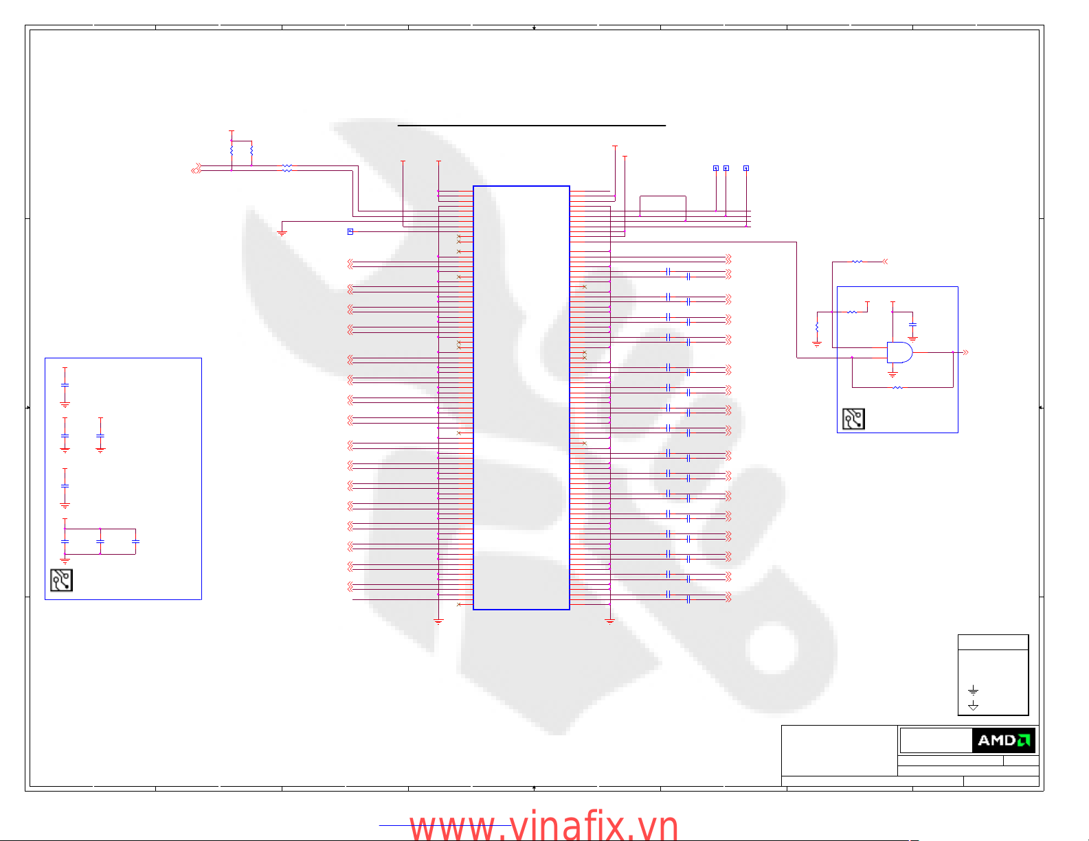
8
7
6
5
4
3
2
1
RV710 CUSTOM
VGA(header) + HDMI + DVI
D D
GPIO_43
GPIO_33
C C
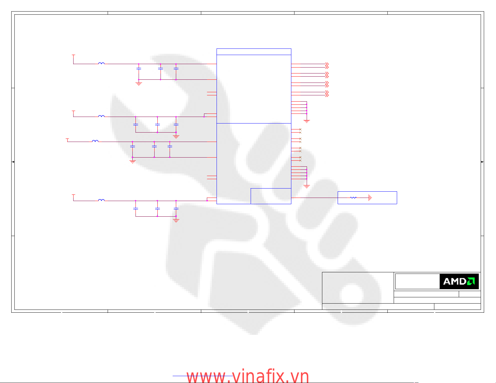
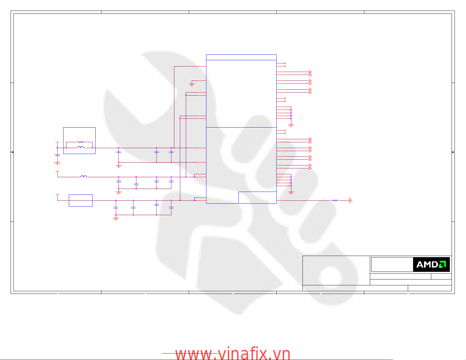
+12V_BUS
C14
C14
CAP CER 10UF 20% 16V X5R
10UF
10UF
(1206)1.8MM H MAX
<New PN>
<New PN>
+12V_BUS
+12V_BUS
C21
C21
C20
C20
150nF_16V
150nF_16V
150nF_16V
150nF_16V
LF CAP CER 150NF 10% 16V X7R (0603)
LF CAP CER 150NF 10% 16V X7R (0603)
C11-1542513-W08
C11-1542513-W08
C11-1542513-W08
C11-1542513-W08
+3.3V_BUS
CAP CER 10UF 10% 6.3V X5R
(0805)1.4MM MAX THICK
C27
C27
10uF
B B
A A
10uF
<New PN>
<New PN>
+3.3V_BUS
C33
C33
1uF_6.3V
1uF_6.3V
C11-1057322-T04
C11-1057322-T04
C34
C34
1uF_6.3V
1uF_6.3V
C11-1057322-T04
C11-1057322-T04
Place these caps last,
ideally as close to the bus
connector as possible
8
C35
C35
10nF
10nF
C11-1032412-S02
C11-1032412-S02
+3.3V
R1
R1
4.7K
4.7K
R11-0472022-W08
R11-0472022-W08
7
R2
R2
4.7K
4.7K
R11-0472022-W08
R11-0472022-W08
<New PN>
<New PN>
<New PN>
<New PN>
SMCLK
DNI
R40R
R40R
SMDAT
DNI
R50R
R50R
TP5 35mil
TP5 35mil
<New PN>
<New PN>
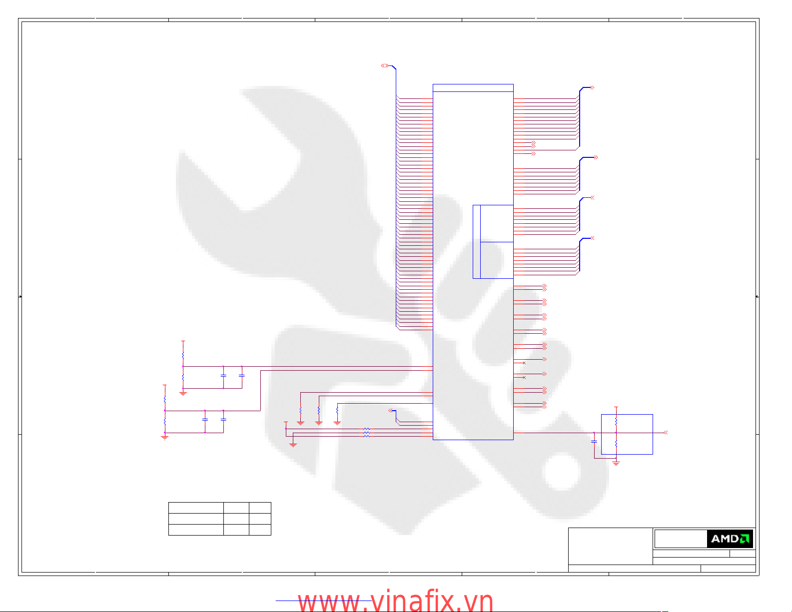
PETn0_GFXRn02
PETp1_GFXRp12
PETn1_GFXRn12
PETp2_GFXRp22
PETn2_GFXRn22
PETp3_GFXRp32
PETn3_GFXRn32
PETp4_GFXRp42
PETn4_GFXRn42
PETp5_GFXRp52
PETn5_GFXRn52
PETp6_GFXRp62
PETn6_GFXRn62
PETp7_GFXRp72
PETn7_GFXRn72
PETp8_GFXRp82
PETn8_GFXRn82
PETp9_GFXRp92
PETn9_GFXRn92
PETp10_GFXRp102
PETn10_GFXRn102
PETp11_GFXRp112
PETn11_GFXRn112
PETp12_GFXRp122
PETn12_GFXRn122
PETp13_GFXRp132
PETn13_GFXRn132
PETp14_GFXRp142
PETn14_GFXRn142
PETp15_GFXRp152
PETn15_GFXRn152
PRESENCE
6
PCI-EXPRESS EDGE CONNECTOR
+12V_BUS
PRESENCE
4
+3.3V_BUS
PERp0
PERn0
PERp1
PERn1
PERp2
PERn2
PERp3
PERn3
PERp4
PERn4
PERp5
PERn5
PERp6
PERn6
PERp7
PERn7
PERp8
PERn8
PERp9
PERn9
PERp10
PERn10
PERp11
PERn11
PERp12
PERn12
PERp13
PERn13
PERp14
PERn14
PERp15
PERn15
JTRST
+12V_BUS+3.3V_BUS
x16 PCIe
x16 PCIe
B1
B2
B3
B4
B5
B6
B7
B8
B9
B10
B11
B12
B13
B14
B15
B16
B17
B18
B19
B20
B21
B22
B23
B24
B25
B26
B27
B28
B29
B30
B31
B32
B33
B34
B35
B36
B37
B38
B39
B40
B41
B42
B43
B44
B45
B46
B47
B48
B49
B50
B51
B52
B53
B54
B55
B56
B57
B58
B59
B60
B61
B62
B63
B64
B65
B66
B67
B68
B69
B70
B71
B72
B73
B74
B75
B76
B77
B78
B79
B80
B81
B82
+12V#B1
+12V#B2
+12V#B3
GND#B4
SMCLK
SMDAT
GND#B7
+3.3V#B8
JTAG1
3.3Vaux
WAKE#
RSVD#B12
GND#B13
PETp0
PETn0
GND#B16
PRSNT2#B17
GND#B18
PETp1
PETn1
GND#B21
GND#B22
PETp2
PETn2
GND#B25
GND#B26
PETp3
PETn3
GND#B29
RSVD#B30
PRSNT2#B31
GND#B32
PETp4
PETn4
GND#B35
GND#B36
PETp5
PETn5
GND#B39
GND#B40
PETp6
PETn6
GND#B43
GND#B44
PETp7
PETn7
GND#B47
PRSNT2#B48
GND#B49
PETp8
PETn8
GND#B52
GND#B53
PETp9
PETn9
GND#B56
GND#B57
PETp10
PETn10
GND#B60
GND#B61
PETp11
PETn11
GND#B64
GND#B65
PETp12
PETn12
GND#B68
GND#B69
PETp13
PETn13
GND#B72
GND#B73
PETp14
PETn14
GND#B76
GND#B77
PETp15
PETn15
GND#B80
PRSNT2#B81
RSVD#B82
<New PN>
<New PN>
5
Mechanical Key
Mechanical Key
PRSNT1#A1
+12V#A2
+12V#A3
GND#A4
JTAG2
JTAG3
JTAG4
JTAG5
+3.3V#A9
+3.3V#A10
PERST#
GND#A12
REFCLK+
REFCLKGND#A15
PERp0
PERn0
GND#A18
RSVD#A19
GND#A20
PERp1
PERn1
GND#A23
GND#A24
PERp2
PERn2
GND#A27
GND#A28
PERp3
PERn3
GND#A31
RSVD#A32
RSVD#A33
GND#A34
PERp4
PERn4
GND#A37
GND#A38
PERp5
PERn5
GND#A41
GND#A42
PERp6
PERn6
GND#A45
GND#A46
PERp7
PERn7
GND#A49
RSVD#A50
GND#A51
PERp8
PERn8
GND#A54
GND#A55
PERp9
PERn9
GND#A58
GND#A59
PERp10
PERn10
GND#A62
GND#A63
PERp11
PERn11
GND#A66
GND#A67
PERp12
PERn12
GND#A70
GND#A71
PERp13
PERn13
GND#A74
GND#A75
PERp14
PERn14
GND#A78
GND#A79
PERp15
PERn15
GND#A82
MPCIE1
MPCIE1
A1
A2
A3
A4
A5
A6
A7
A8
A9
A10
A11
A12
A13
A14
A15
A16
A17
A18
A19
A20
A21
A22
A23
A24
A25
A26
A27
A28
A29
A30
A31
A32
A33
A34
A35
A36
A37
A38
A39
A40
A41
A42
A43
A44
A45
A46
A47
A48
A49
A50
A51
A52
A53
A54
A55
A56
A57
A58
A59
A60
A61
A62
A63
A64
A65
A66
A67
A68
A69
A70
A71
A72
A73
A74
A75
A76
A77
A78
A79
A80
A81
A82
C3
C3
100nF
100nF
C11-1047412-S02
C11-1047412-S02
C11-1047412-S02
C11-1047412-S02
C5
C5
100nF
100nF
C11-1047412-S02
C11-1047412-S02
C11-1047412-S02
C11-1047412-S02
C7
C7
100nF
100nF
C11-1047412-S02
C11-1047412-S02
C11-1047412-S02
C11-1047412-S02
C10
C10
100nF
100nF
C11-1047412-S02
C11-1047412-S02
C11-1047412-S02
C11-1047412-S02
C12
C12
100nF
100nF
C11-1047412-S02
C11-1047412-S02
C11-1047412-S02
C11-1047412-S02
C15
C15
100nF
100nF
C11-1047412-S02
C11-1047412-S02
C11-1047412-S02
C11-1047412-S02
C17
C17
100nF
100nF
C11-1047412-S02
C11-1047412-S02
C11-1047412-S02
C11-1047412-S02
C19
C19
100nF
100nF
C11-1047412-S02
C11-1047412-S02
C11-1047412-S02
C11-1047412-S02
C23
C23
100nF
100nF
C11-1047412-S02
C11-1047412-S02
C11-1047412-S02
C11-1047412-S02
C25
C25
100nF
100nF
C11-1047412-S02
C11-1047412-S02
C11-1047412-S02
C11-1047412-S02
C28
C28
100nF
100nF
C11-1047412-S02
C11-1047412-S02
C11-1047412-S02
C11-1047412-S02
C30
C30
100nF
100nF
C11-1047412-S02
C11-1047412-S02
C11-1047412-S02
C11-1047412-S02
C32
C32
100nF
100nF
C11-1047412-S02
C11-1047412-S02
C11-1047412-S02
C11-1047412-S02
C37
C37
100nF
100nF
C11-1047412-S02
C11-1047412-S02
C11-1047412-S02
C11-1047412-S02
C39
C39
100nF
100nF
C11-1047412-S02
C11-1047412-S02
C11-1047412-S02
C11-1047412-S02
C41
C41
100nF
100nF
C11-1047412-S02
C11-1047412-S02
C11-1047412-S02
C11-1047412-S02
C4
C4
100nF
100nF
C6
C6
100nF
100nF
C9
C9
100nF
100nF
C11
C11
100nF
100nF
C13
C13
100nF
100nF
C16
C16
100nF
100nF
C18
C18
100nF
100nF
C22
C22
100nF
100nF
C24
C24
100nF
100nF
C26
C26
100nF
100nF
C29
C29
100nF
100nF
C31
C31
100nF
100nF
C36
C36
100nF
100nF
C38
C38
100nF
100nF
C40
C40
100nF
100nF
C42
C42
100nF
100nF
TP1
TP1
TP4
TP4
TP2
TP2
35mil
35mil
35mil
35mil
35mil
35mil
<New PN>
<New PN>
<New PN>
<New PN>
<New PN>
<New PN>
JTCK
JTDI
JTDO
JTMS
PERST#
PCIE_REFCLKP 2
PCIE_REFCLKN 2PETp0_GFXRp02
GFXTp0_PERp0 2
GFXTn0_PERn0 2
GFXTp1_PERp1 2
GFXTn1_PERn1 2
GFXTp2_PERp2 2
GFXTn2_PERn2 2
GFXTp3_PERp3 2
GFXTn3_PERn3 2
GFXTp4_PERp4 2
GFXTn4_PERn4 2
GFXTp5_PERp5 2
GFXTn5_PERn5 2
GFXTp6_PERp6 2
GFXTn6_PERn6 2
GFXTp7_PERp7 2
GFXTn7_PERn7 2
GFXTp8_PERp8 2
GFXTn8_PERn8 2
GFXTp9_PERp9 2
GFXTn9_PERn9 2
GFXTp10_PERp10 2
GFXTn10_PERn10 2
GFXTp11_PERp11 2
GFXTn11_PERn11 2
GFXTp12_PERp12 2
GFXTn12_PERn12 2
GFXTp13_PERp13 2
GFXTn13_PERn13 2
GFXTp14_PERp14 2
GFXTn14_PERn14 2
GFXTp15_PERp15 2
GFXTn15_PERn15 2
3
CONFIDENTIAL & PROPRIETARY TO ADVANCED MICRO DEVICES INC.
CONFIDENTIAL & PROPRIETARY TO ADVANCED MICRO DEVICES INC.
CONFIDENTIAL & PROPRIETARY TO ADVANCED MICRO DEVICES INC.
?2007 Advanced Micro Devices
?2007 Advanced Micro Devices
?2007 Advanced Micro Devices
This AMD Board schematic and design is the exclusive property of AMD,
This AMD Board schematic and design is the exclusive property of AMD,
This AMD Board schematic and design is the exclusive property of AMD,
and is provided only to entities under a non-disclosure agreement
and is provided only to entities under a non-disclosure agreement
and is provided only to entities under a non-disclosure agreement
with AMD for evaluation purposes. Further distribution or disclosure
with AMD for evaluation purposes. Further distribution or disclosure
with AMD for evaluation purposes. Further distribution or disclosure
is strictly prohibited. Use of this schematic and design for any purpose
is strictly prohibited. Use of this schematic and design for any purpose
is strictly prohibited. Use of this schematic and design for any purpose
other than evaluation requires a Board Technology License Agreement
other than evaluation requires a Board Technology License Agreement
other than evaluation requires a Board Technology License Agreement
with AMD. AMD makes no representations or warranties of any kind
with AMD. AMD makes no representations or warranties of any kind
with AMD. AMD makes no representations or warranties of any kind
regarding this schematic and design, including, not limited to,
regarding this schematic and design, including, not limited to,
regarding this schematic and design, including, not limited to,
any implied warranty of merchantibility or fitness for a particular
any implied warranty of merchantibility or fitness for a particular
any implied warranty of merchantibility or fitness for a particular
purpose, and disclaims responsibility forany consequences resulting
purpose, and disclaims responsibility forany consequences resulting
purpose, and disclaims responsibility forany consequences resulting
from use of the information included herein.
from use of the information included herein.
from use of the information included herein.
Title
Title
Title
RH LP RV710 DDR3 VGA (header) TVO DVI
RH LP RV710 DDR3 VGA (header) TVO DVI
RH LP RV710 DDR3 VGA (header) TVO DVI
<New PN>
<New PN>
R64
R64
1K
1K
R65 0R
R65 0R
R11-0000012-Y01
R11-0000012-Y01
R63 0R
R63 0R
<New PN>
<New PN>
2
+3.3V
Place R61 in U4
PWR_GOOD 4,13,14
+3.3V_BUS
53
C11-1047412-S02
C11-1047412-S02
1
2
T39-01G0800-N47
T39-01G0800-N47
R61 0R
R61 0R
DNI
<New PN>
<New PN>
Advanced Micro Devices Inc.
Advanced Micro Devices Inc.
Advanced Micro Devices Inc.
1 Commerce Valley Drive East
1 Commerce Valley Drive East
1 Commerce Valley Drive East
Markham, Ontario
Markham, Ontario
Markham, Ontario
Wednesday, November 19, 2008
Wednesday, November 19, 2008
Wednesday, November 19, 2008
Sheet
Sheet
Sheet
C8
C8
100nF
100nF
4
U4
U4
NC7SZ08P5X_NL
NC7SZ08P5X_NL
of
1 25
of
1 25
of
1 25
PERST#_buf 2,20
SYMBOL LEGEND
DNI
#
Doc No.
Doc No.
Doc No.
105-B758XX-00B
105-B758XX-00B
105-B758XX-00B
1
DO NOT
INSTALL
ACTIVE
LOW
DIGITAL
GROUND
ANALOG
GROUND
RevDate:
RevDate:
RevDate:
1
1
1
PDF 文件使用 "pdfFactory Pro" 试用版本创建 www.fineprint.cn
www.vinafix.vn
Page 2
5
D D
NOTE: some of the PCIE testpoints will
be available through via on traces.
PETp0_GFXRp01
PETn0_GFXRn01
PETp1_GFXRp11
PETn1_GFXRn11
PETp2_GFXRp21
PETn2_GFXRn21
PETp3_GFXRp31
PETn3_GFXRn31
PETp4_GFXRp41
PETn4_GFXRn41
PETp5_GFXRp51
PETn5_GFXRn51
PETp6_GFXRp61
C C
B B
PETn6_GFXRn61
PETp7_GFXRp71
PETn7_GFXRn71
PETp8_GFXRp81
PETn8_GFXRn81
PETp9_GFXRp91
PETn9_GFXRn91
PETp10_GFXRp101
PETn10_GFXRn101
PETp11_GFXRp111
PETn11_GFXRn111
PETp12_GFXRp121
PETn12_GFXRn121
PETp13_GFXRp131
PETn13_GFXRn131
PETp14_GFXRp141
PETn14_GFXRn141
PETp15_GFXRp151
PETn15_GFXRn151
PCIE_REFCLKP1
PCIE_REFCLKN1
DNI DNI
R10
R10
R11
R11
51R
51R
51R
51R
402 402
<New PN>
<New PN>
<New PN>
<New PN>
For Tektronix LA only
Place close
to ASIC
<New PN>
<New PN>
<New PN>
<New PN>
<New PN>
<New PN>
<New PN>
<New PN>
<New PN>
<New PN>
<New PN>
<New PN>
<New PN>
<New PN>
<New PN>
<New PN>
<New PN>
<New PN>
<New PN>
<New PN>
PERST#_buf1,20
4
U1A
U1A
PART 1 OF 10
PART 1 OF 10
TP7
TP7
<New PN>
<New PN>
TP8
TP8
<New PN>
<New PN>
TP9
TP9
<New PN>
<New PN>
TP10
TP10
TP11
TP11
<New PN>
<New PN>
TP12
TP12
TP13
TP13
TP15
TP15
TP14
TP14
<New PN>
<New PN>
TP16
TP16
<New PN>
<New PN>
TP17
TP17
<New PN>
<New PN>
TP18
TP18
TP19
TP19
<New PN>
<New PN>
TP20
TP20
TP21
TP21
TP22
TP22
TP23
TP23
<New PN>
<New PN>
TP24
TP24
<New PN>
<New PN>
TP25
TP25
<New PN>
<New PN>
TP27
TP27
TP26
TP26
<New PN>
<New PN>
TP28
TP28
AF30
PCIE_RX0P
AE31
PCIE_RX0N
AE29
PCIE_RX1P
AD28
PCIE_RX1N
AD30
PCIE_RX2P
AC31
PCIE_RX2N
AC29
PCIE_RX3P
AB28
PCIE_RX3N
AB30
PCIE_RX4P
AA31
PCIE_RX4N
AA29
PCIE_RX5P
Y28
PCIE_RX5N
Y30
PCIE_RX6P
W31
PCIE_RX6N
W29
PCIE_RX7P
V28
PCIE_RX7N
V30
PCIE_RX8P
U31
PCIE_RX8N
U29
PCIE_RX9P
T28
PCIE_RX9N
T30
PCIE_RX10P
R31
PCIE_RX10N
R29
PCIE_RX11P
P28
PCIE_RX11N
P30
PCIE_RX12P
N31
PCIE_RX12N
N29
PCIE_RX13P
M28
PCIE_RX13N
M30
PCIE_RX14P
L31
PCIE_RX14N
L29
PCIE_RX15P
K30
PCIE_RX15N
AK30
PCIE_REFCLKP
AK32
PCIE_REFCLKN
AL27
PERSTB
RV710 A11 HF MVD FT1 BIN1
RV710 A11 HF MVD FT1 BIN1
B03-RV71005-A08
B03-RV71005-A08
PCI-EXPRESS INTERFACE
PCI-EXPRESS INTERFACE
PCIE_TX0P
PCIE_TX0N
PCIE_TX1P
PCIE_TX1N
PCIE_TX2P
PCIE_TX2N
PCIE_TX3P
PCIE_TX3N
PCIE_TX4P
PCIE_TX4N
PCIE_TX5P
PCIE_TX5N
PCIE_TX6P
PCIE_TX6N
PCIE_TX7P
PCIE_TX7N
PCIE_TX8P
PCIE_TX8N
PCIE_TX9P
PCIE_TX9N
PCIE_TX10P
PCIE_TX10N
PCIE_TX11P
PCIE_TX11N
PCIE_TX12P
PCIE_TX12N
PCIE_TX13P
PCIE_TX13N
PCIE_TX14P
PCIE_TX14N
PCIE_TX15P
PCIE_TX15N
PCIE_CALRN
PCIE_CALRP
3
AH30
AG31
AG29
AF28
AF27
AF26
AD27
AD26
AC25
AB25
Y23
Y24
AB27
AB26
Y27
Y26
W24
W23
V27
U26
U24
U23
T26
T27
T24
T23
P27
P26
P24
P23
M27
N26
AA22
Y22
PCIE_CALRN
PCIE_CALRP
R11-0202T22-C36
R11-0202T22-C36
R11-1271T12-W08
R11-1271T12-W08
+1.1V
402
R82.0K
R82.0K
402
R91.27K
R91.27K
2
GFXTp0_PERp0 1
GFXTn0_PERn0 1
GFXTp1_PERp1 1
GFXTn1_PERn1 1
GFXTp2_PERp2 1
GFXTn2_PERn2 1
GFXTp3_PERp3 1
GFXTn3_PERn3 1
GFXTp4_PERp4 1
GFXTn4_PERn4 1
GFXTp5_PERp5 1
GFXTn5_PERn5 1
GFXTp6_PERp6 1
GFXTn6_PERn6 1
GFXTp7_PERp7 1
GFXTn7_PERn7 1
GFXTp8_PERp8 1
GFXTn8_PERn8 1
GFXTp9_PERp9 1
GFXTn9_PERn9 1
GFXTp10_PERp10 1
GFXTn10_PERn10 1
GFXTp11_PERp11 1
GFXTn11_PERn11 1
GFXTp12_PERp12 1
GFXTn12_PERn12 1
GFXTp13_PERp13 1
GFXTn13_PERn13 1
GFXTp14_PERp14 1
GFXTn14_PERn14 1
GFXTp15_PERp15 1
GFXTn15_PERn15 1
1
A A
CONFIDENTIAL & PROPRIETARY TO ADVANCED MICRO DEVICES INC.
CONFIDENTIAL & PROPRIETARY TO ADVANCED MICRO DEVICES INC.
CONFIDENTIAL & PROPRIETARY TO ADVANCED MICRO DEVICES INC.
?2007 Advanced Micro Devices
?2007 Advanced Micro Devices
?2007 Advanced Micro Devices
This AMD Board schematic and design is the exclusive property of AMD,
This AMD Board schematic and design is the exclusive property of AMD,
This AMD Board schematic and design is the exclusive property of AMD,
and is provided only to entities under a non-disclosure agreement
and is provided only to entities under a non-disclosure agreement
and is provided only to entities under a non-disclosure agreement
with AMD for evaluation purposes. Further distribution or disclosure
with AMD for evaluation purposes. Further distribution or disclosure
with AMD for evaluation purposes. Further distribution or disclosure
is strictly prohibited. Use of this schematic and design for any purpose
is strictly prohibited. Use of this schematic and design for any purpose
is strictly prohibited. Use of this schematic and design for any purpose
other than evaluation requires a Board Technology License Agreement
other than evaluation requires a Board Technology License Agreement
other than evaluation requires a Board Technology License Agreement
with AMD. AMD makes no representations or warranties of any kind
with AMD. AMD makes no representations or warranties of any kind
with AMD. AMD makes no representations or warranties of any kind
regarding this schematic and design, including, not limited to,
regarding this schematic and design, including, not limited to,
regarding this schematic and design, including, not limited to,
any implied warranty of merchantibility or fitness for a particular
any implied warranty of merchantibility or fitness for a particular
any implied warranty of merchantibility or fitness for a particular
purpose, and disclaims responsibility forany consequences resulting
purpose, and disclaims responsibility forany consequences resulting
purpose, and disclaims responsibility forany consequences resulting
from use of the information included herein.
from use of the information included herein.
from use of the information included herein.
Title
Title
Title
RH LP RV710 DDR3 VGA (header) TVO DVI
RH LP RV710 DDR3 VGA (header) TVO DVI
5
4
3
2
RH LP RV710 DDR3 VGA (header) TVO DVI
Advanced Micro Devices Inc.
Advanced Micro Devices Inc.
Advanced Micro Devices Inc.
1 Commerce Valley Drive East
1 Commerce Valley Drive East
1 Commerce Valley Drive East
Markham, Ontario
Markham, Ontario
Markham, Ontario
Wednesday, November 19, 2008
Wednesday, November 19, 2008
Wednesday, November 19, 2008
Sheet
Sheet
Sheet
of
2 25
of
2 25
of
2 25
1
Doc No.
Doc No.
Doc No.
RevDate:
RevDate:
RevDate:
1
1
1
105-B758XX-00B
105-B758XX-00B
105-B758XX-00B
PDF 文件使用 "pdfFactory Pro" 试用版本创建 www.fineprint.cn
www.vinafix.vn
Page 3
5
D D
<New PN>
<New PN>
<New PN>
<New PN>
<New PN>
<New PN>
<New PN>
<New PN>
<New PN>
<New PN>
R21 221R
R21 221R
R11-2210T12-C36
R11-2210T12-C36
R22 110R
R22 110R
C53 100nF
C53 100nF
R11-0111T22-C36
R11-0111T22-C36
C11-1047412-S02
C11-1047412-S02
GPIO_0
GPIO_1
GPIO_2
GPIO_3
GPIO_4
GPIO_5
PWRCNTL_2
GPIO_7
GPIO8_SO
GPIO9_SI
GPIO10_SCK
GPIO_11
GPIO_12
GPIO_13
HPD2
PWRCNTL_0
GPIO_16
ThermINT
HPD3
CTF
PWRCNTL_1
GPIO21_BB_ENA
GPIO_22_CS
GPIO_23
JTAG_TRSTB
JTAG_TDI
JTAG_TCK
JTAG_TMS
JTAG_TDO
GENERICB
GENERICC
GENERICD
HPD1
R35
R35
GPIO_010
GPIO_110
GPIO_210
GPIO_31
C C
PWRCNTL_214
TP52 35mil
TP52 35mil
<New PN>
<New PN>
TP48 35mil
TP48 35mil
<New PN>
<New PN>
TP51
TP51
TP43
TP43
<New PN>
<New PN>
<New PN>
<New PN>
TP50
TP50
<New PN>
<New PN>
B B
A A
GPIO_41
GPIO_510
GPIO_710
GPIO_8
R13 33R
5
GPIO_9
GPIO_10
GPIO_22
R13 33R
R14 33R
R14 33R
R15 33R
R15 33R
R11-0330032-Y01
R11-0330032-Y01
R11-0330032-Y01
R11-0330032-Y01
R11-0330032-Y01
R11-0330032-Y01
R16 33R
R16 33R
R11-0330032-Y01
R11-0330032-Y01
+1.8V
R62
R62
1K
1K
R11-0102032-W08
R11-0102032-W08
TP30
TP30
TP44 35mil
TP44 35mil
TP45 35mil
TP45 35mil
TP46 35mil
TP46 35mil
TP47 35mil
TP47 35mil
GPIO_810
GPIO_9
GPIO_1110
GPIO_1210
GPIO_1310
PWRCNTL_014
GPIO_1610
CTF20
PWRCNTL_114
TP40
TP40
TP41
TP41
<New PN>
<New PN>
TP42
TP42
<New PN>
<New PN>
HPD416
<New PN>
<New PN>
HPD118
VREFG
Removed
1K
1K
R11-0102032-W08
R11-0102032-W08
4
U1B
U1B
U1
DVPCLK
AC7
DVPCNTL_0
Y2
DVPCNTL_1
U5
DVPCNTL_2
AA1
DVPCNTL_MVP_0
Y4
DVPCNTL_MVP_1
Y7
DVPDATA_0
V2
DVPDATA_1
Y8
DVPDATA_2
V4
DVPDATA_3
AB7
DVPDATA_4
W1
DVPDATA_5
AB8
DVPDATA_6
W3
DVPDATA_7
AB9
DVPDATA_8
W5
DVPDATA_9
AC6
DVPDATA_10
W6
DVPDATA_11
AD7
DVPDATA_12
AA3
DVPDATA_13
AC8
DVPDATA_14
AA5
DVPDATA_15
AE8
DVPDATA_16
AA6
DVPDATA_17
AE9
DVPDATA_18
AB4
DVPDATA_19
AD9
DVPDATA_20
AB2
DVPDATA_21
AC10
DVPDATA_22
AC5
DVPDATA_23
U6
GPIO_0
U10
GPIO_1
T10
GPIO_2
U8
GPIO_3_SMBDATA
U7
GPIO_4_SMBCLK
T9
GPIO_5_AC_BATT
T8
GPIO_6_TACH
T7
GPIO_7_BLON
P10
GPIO_8_ROMSO
P4
GPIO_9_ROMSI
P2
GPIO_10_ROMSCK
N6
GPIO_11
N5
GPIO_12
N3
GPIO_13
Y9
GPIO_14_HPD2
N1
GPIO_15_PWRCNTL_0
M4
GPIO_16_SSIN
R6
GPIO_17_THERMAL_INT
W10
GPIO_18_HPD3
M2
GPIO_19_CTF
P8
GPIO_20_PWRCNTL_1
P7
GPIO_21_BB_EN
N8
GPIO_22_ROMCSB
N7
GPIO_23_CLKREQB
L6
JTAG_TRSTB
L5
JTAG_TDI
L3
JTAG_TCK
L1
JTAG_TMS
K4
JTAG_TDO
AB13
GENERICA
W8
GENERICB
W9
GENERICC
W7
GENERICD
AD10
GENERICE_HPD4
AC14
HPD1
AC16
VREFG
N10
NC_PWRGOOD
AB22
RSVD#8
AC22
RSVD#9
L9
NC#1
N9
NC#2
AB16
RSVD#3
AB12
RSVD#2
AB11
RSVD#1
AF24
TESTEN
RV710 A11 HF MVD FT1 BIN1
RV710 A11 HF MVD FT1 BIN1
B03-RV71005-A08
B03-RV71005-A08
4
RESERVED
RESERVED
PART 2 OF 10
PART 2 OF 10
DVP PORT DAC1
DVP PORT DAC1
I/O
I/O
3
AM26
R
AK26
RB
AL25
G
AJ25
GB
AH24
B
AG25
BB
AH26
HSYNC
AJ27
VSYNC
AG24
AVDD
AE22
AVSSQ
AE23
VDD1DI
AD23
VSS1DI
RSET
AD22
RSET
DAC2
DAC2
AM12
R2
AK12
R2B
AL11
G2
AJ11
G2B
AK10
B2
AL9
B2B
AL13
H2SYNC
AJ13
V2SYNC
AH12
C
AM10
Y
AJ9
COMP
AE20
A2VDD
AE17
A2VDDQ
AE19
A2VSSQ
AD19
VDD2DI
AC19
VSS2DI
AG13
R2SET
+A2VDD
R2SET
R12 499R
R12 499R
R11-4990T12-Y01
R11-4990T12-Y01
R23 715R
R23 715R
R11-7150T12-W08
R11-7150T12-W08
A_R_DAC1 16
A_RB_DAC1 16
A_G_DAC1 16
A_GB_DAC1 16
A_B_DAC1 16
A_BB_DAC1 16
A_HSYNC_DAC1 10,16
A_VSYNC_DAC1 10,16
A_R_DAC2 17
A_RB_DAC2 17
A_G_DAC2 17
A_GB_DAC2 17
A_B_DAC2 17
A_BB_DAC2 17
A_HSYNC_DAC2 10,17
A_VSYNC_DAC2 17
3
DNI
C1050
C1050
10nF
10nF
10VX7R
40210%
C11-1032412-S02
C11-1032412-S02
DNI
C1053
C1053
10nF
10nF
10V
40210%
C11-1032412-S02
C11-1032412-S02
Place very close to ASIC balls.
C1052
C1052
C1051
C1051
100nF
100nF
1uF_6.3V
1uF_6.3V
10VX5R
6.3V
402
10%
402 10%
C11-1057322-T04
C11-1057322-T04
C11-1047412-S02
C11-1047412-S02
C1055
C1055
C1054
C1054
100nF
100nF
1uF_6.3V
1uF_6.3V
X7R 10VX5R
6.3VX5R
40210%
402 10%
C11-1057322-T04
C11-1057322-T04
C11-1047412-S02
C11-1047412-S02
C2058
C2058
10nF
10nF
C11-1032412-S02
C11-1032412-S02
C2052
C2052
100nF
100nF
C11-1047412-S02
C11-1047412-S02
C2054
C2054
10nF
10nF
C11-1032412-S02
C11-1032412-S02
Place very close to ASIC balls.
X5R
C11-4757313-T04
C11-4757313-T04
C2051
C2051
100nF
100nF
C11-1047412-S02
C11-1047412-S02
C2053
C2053
1uF_6.3V
1uF_6.3V
C11-1057322-T04
C11-1057322-T04
C2055
C2055
100nF
100nF
C11-1047412-S02
C11-1047412-S02
C1056
C1056
4.7uF_6.3V
4.7uF_6.3V
C2050
C2050
1uF_6.3V
1uF_6.3V
C11-1057322-T04
C11-1057322-T04
C2056
C2056
1uF_6.3V
1uF_6.3V
C11-1057322-T04
C11-1057322-T04
+1.8V_DAC
+1.8V_DAC
C2057
C2057
4.7uF_6.3V
4.7uF_6.3V
C11-4757313-T04
C11-4757313-T04
B3 120R_300mA
B3 120R_300mA
L02-1218072-C08
L02-1218072-C08
+1.8V_DAC
+1.8V_DAC
2
2
+3.3V
GPIO_22
GPIO_8
B1 BLM15BD121SN1
B1 BLM15BD121SN1
L02-1218012-M09
L02-1218012-M09
+3.3V
+3.3V
R11-0102032-W08
R11-0102032-W08
ROM_WP
CONFIDENTIAL & PROPRIETARY TO ADVANCED MICRO DEVICES INC.
CONFIDENTIAL & PROPRIETARY TO ADVANCED MICRO DEVICES INC.
CONFIDENTIAL & PROPRIETARY TO ADVANCED MICRO DEVICES INC.
?2007 Advanced Micro Devices
?2007 Advanced Micro Devices
?2007 Advanced Micro Devices
This AMD Board schematic and design is the exclusive property of AMD,
This AMD Board schematic and design is the exclusive property of AMD,
This AMD Board schematic and design is the exclusive property of AMD,
and is provided only to entities under a non-disclosure agreement
and is provided only to entities under a non-disclosure agreement
and is provided only to entities under a non-disclosure agreement
with AMD for evaluation purposes. Further distribution or disclosure
with AMD for evaluation purposes. Further distribution or disclosure
with AMD for evaluation purposes. Further distribution or disclosure
is strictly prohibited. Use of this schematic and design for any purpose
is strictly prohibited. Use of this schematic and design for any purpose
is strictly prohibited. Use of this schematic and design for any purpose
other than evaluation requires a Board Technology License Agreement
other than evaluation requires a Board Technology License Agreement
other than evaluation requires a Board Technology License Agreement
with AMD. AMD makes no representations or warranties of any kind
with AMD. AMD makes no representations or warranties of any kind
with AMD. AMD makes no representations or warranties of any kind
regarding this schematic and design, including, not limited to,
regarding this schematic and design, including, not limited to,
regarding this schematic and design, including, not limited to,
any implied warranty of merchantibility or fitness for a particular
any implied warranty of merchantibility or fitness for a particular
any implied warranty of merchantibility or fitness for a particular
purpose, and disclaims responsibility forany consequences resulting
purpose, and disclaims responsibility forany consequences resulting
purpose, and disclaims responsibility forany consequences resulting
from use of the information included herein.
from use of the information included herein.
from use of the information included herein.
Title
Title
Title
RH LP RV710 DDR3 VGA (header) TVO DVI
RH LP RV710 DDR3 VGA (header) TVO DVI
RH LP RV710 DDR3 VGA (header) TVO DVI
+1.8V+1.8V_DAC
R24
R24
1K
1K
U2
U2
1
CE#
2
SO
3
WP#
GND4SI
PM25LV512A-100SCE
PM25LV512A-100SCE
M31-2551243-P81
M31-2551243-P81
1
8
VCC
7
HOLD#
GPIO_10
6
SCK
GPIO_9
5
Advanced Micro Devices Inc.
Advanced Micro Devices Inc.
Advanced Micro Devices Inc.
1 Commerce Valley Drive East
1 Commerce Valley Drive East
1 Commerce Valley Drive East
Markham, Ontario
Markham, Ontario
Markham, Ontario
Wednesday, November 19, 2008
Wednesday, November 19, 2008
Wednesday, November 19, 2008
Sheet
Sheet
Sheet
of
3 25
of
3 25
of
3 25
1
Doc No.
Doc No.
Doc No.
+3.3V
C57
C57
100nF
100nF
C11-1047412-S02
C11-1047412-S02
RevDate:
RevDate:
RevDate:
1
1
1
105-B758XX-00B
105-B758XX-00B
105-B758XX-00B
PDF 文件使用 "pdfFactory Pro" 试用版本创建 www.fineprint.cn
www.vinafix.vn
Page 4
5
RV710: Do not install B6, C60, C61, C62, C58.
D D
C C
+3.3V_BUS
R25
R25
5.1K
5.1K
PWR_GOOD1,13,14
R11-0512022-C36
R11-0512022-C36
C82
C82
12pF_50V
12pF_50V
C11-1201832-A15
C11-1201832-A15
C83
C83
12pF_50V
12pF_50V
C11-1201832-A15
C11-1201832-A15
+3.3V_BUS
RV810: Install B6, C60, C61, C62, C58..
+1.8V
B6
B6
BLM15BD121SN1
BLM15BD121SN1
DNI
NS6 NS_VIA
NS6 NS_VIA
1 2
<New PN>
<New PN>
+1.1V
+VDDC
RV710: Install B10, do not install B9
RV810: Install B9, do not install B10
May overlap a pad
XTALIN_S
2 1
Y2
Y2
27.000MHz_10PPM
27.000MHz_10PPM
D04-1103000-N38
D04-1103000-N38
DNI
B13
B13
BLM15BD121SN1
BLM15BD121SN1
DNI
<New PN>
<New PN>
C76
C76
1uF_6.3V
1uF_6.3V
<New PN>
<New PN>
<New PN>
<New PN>
4.7uF_6.3V
4.7uF_6.3V
B9
B9
B10
B10
DNIDNI
<New PN>
<New PN>
4
Overlap
C60
C60
C61
MC58
MC58
C58
C58
10uF_X6S
10uF_X6S
DNI DNI DNI DNI DNI
<New PN>
<New PN>
<New PN>
<New PN>
DNI
BLM15BD121SN1
BLM15BD121SN1
<New PN>
<New PN>
BLM15BD121SN1
BLM15BD121SN1
L02-1218012-M09
L02-1218012-M09
remove?
Y1
C78
C78
100nF
100nF
4
2
Y1
VCC
GND
27.000MHz
27.000MHz
DNI
<New PN>
<New PN>
OSC_PWR
C61
1uF_6.3V
1uF_6.3V
1uF_6.3V
1uF_6.3V
<New PN>
<New PN>
<New PN>
<New PN>
GND_SPVSS
C71
C71
C70
C70
C69
C69
1uF_6.3V
1uF_6.3V
C11-105A312-M09
C11-105A312-M09
XTALIN_S
XTALOUT
OUT
E/D
Alternate 1.8V oscillator: 501D270000G
1uF_6.3V
1uF_6.3V
3
1
C11-105A312-M09
C11-105A312-M09
R11-0105T12-W08
R11-0105T12-W08
R38
R38
0R
0R
DNI
OSC_OUT
<New PN>
<New PN>
100nF
100nF
R30 182R
R30 182R
R31
R31
1M
1M
PWR_GOOD 1,13,14
+SPV18
C62
C62
100nF
100nF
C11-1047412-S02
C11-1047412-S02
R11-0000012-Y01
R11-0000012-Y01
Populate R38 when using an oscillator.
When using a crystal, trace stray capacitance
can be reduced by not populating R38. The
effect is layout dependent.
<New PN>
<New PN>
C72
C72
10nF
10nF
C11-1032412-S02
C11-1032412-S02
<New PN>
<New PN>
R29
R29
221R
221R
DNI
GND_SPVSS
+SPV10
XTALIN
XTALOUT
U1J
U1J
H7
NC_SPV18
J7
SPVSS
H8
SPV10
AM28
XTALIN
AK28
XTALOUT
RV710 A11 HF MVD FT1 BIN1
RV710 A11 HF MVD FT1 BIN1
B03-RV71005-A08
B03-RV71005-A08
3
Part 10 of 10
Part 10 of 10
XTAL / PLL
XTAL / PLL
DPLL_PVDD
DPLL_PVSS
DPLL_VDDC
PCIE_PVDD
NC_MPV18
AF14
AE14
AD14
AM30
L8
+DPLL_PVDD
+DPLL_VDDC
+PCIE_PVDD
+MPVDD
1uF_6.3V
1uF_6.3V
GND_PVSS
C73
C73
C11-105A312-M09
C11-105A312-M09
2
C59
C59
10nF
10nF
DNI
GND_PVSS
C65
C65
10nF
10nF
DNI
C11-1032412-S02
C11-1032412-S02
C74
C74
10nF
10nF
<New PN>
<New PN>
C64
C64
100nF
100nF
10uF_X6S
10uF_X6S
C11-1047412-S02
C11-1047412-S02
C11-1032412-S02
C11-1032412-S02
C66
C66
C67
C67
100nF
100nF
1uF_6.3V
1uF_6.3V
C11-1047412-S02
C11-1047412-S02
C11-105A312-M09
C11-105A312-M09
Overlap
C75
C75
100nF
100nF
10uF_X6S
10uF_X6S
C11-1047412-S02
C11-1047412-S02
C11-1032412-S02
C11-1032412-S02
C80
C80
C79
C79
100nF
100nF
1uF_6.3V
1uF_6.3V
<New PN>
<New PN>
<New PN>
<New PN>
RV710: Do not install B12, C77, C79, C80, C81.
RV810: Install B12, C77, C79, C80, C81.
Overlap Overlap
MC63
MC63
C88
4.7uF_6.3V
4.7uF_6.3V
C11-106A334-S02
C11-106A334-S02
MC89
MC89
4.7uF_6.3V
4.7uF_6.3V
C77
C77
10uF_X6S
10uF_X6S
<New PN>
<New PN>
C88
10uF_X6S
10uF_X6S
<New PN>
<New PN>
MC68
MC68
4.7uF_6.3V
4.7uF_6.3V
<New PN>
<New PN>
C11-4757313-T04
C11-4757313-T04
MC77
MC77
4.7uF_6.3V
4.7uF_6.3V
DNIDNIDNIDNIDNI
<New PN>
<New PN>
C63
C63
C89
C89
C81
C81
1uF_6.3V
1uF_6.3V
C11-106A334-S02
C11-106A334-S02
Overlap
C68
C68
10uF_X6S
10uF_X6S
<New PN>
<New PN>
C11-106A334-S02
C11-106A334-S02
L02-1218012-M09
L02-1218012-M09
Overlap
MC88
MC88
4.7uF_6.3V
4.7uF_6.3V
<New PN>
<New PN>
Bead removed
B11
B11
BLM15BD121SN1
BLM15BD121SN1
<New PN>
<New PN>
1
+1.8V
Bead removed
NS5NS_VIA
NS5NS_VIA
12
<New PN>
<New PN>
+1.1V
+1.8V
+1.8V
B1260R
B1260R
DNI
+3.3V
R36
SCL
SDA
C4021
C4021
100nF
100nF
R36
4.7K
4.7K
R11-0472022-W08
R11-0472022-W08
+3.3V
R33
R33
4.7K
4.7K
R11-0472022-W08
R11-0472022-W08
GND
C11-1047412-S02
C11-1047412-S02
DDC6 BUS:
B B
A A
5
I2C Address Function Device
0x90 DS4402I2C VDDC Control
0x98 LM63 - External
Temperature Sensor
SCL / SDA BUS:
I2C Address Function Device
N/A N/A N/A
LM63
+1.8V
4
Bead removed
DDC6CLK
DDC6DATA
1uF_6.3V
1uF_6.3V
C4020
C4020
C11-1057322-T04
C11-1057322-T04
R37
R37
4.7K
4.7K
AC1
R11-0472022-W08
R11-0472022-W08
AC3
R34
R34
4.7K
4.7K
R11-0472022-W08
R11-0472022-W08
U1H
U1H
I2C / DDC / AUX
I2C / DDC / AUX
DDC6CLK
DDC6DATA
R1
SCL
R3
SDA
RV710 A11 HF MVD FT1 BIN1
RV710 A11 HF MVD FT1 BIN1
B03-RV71005-A08
B03-RV71005-A08
U1I
U1I
AD17
TSVDD
AC17
TSVSS
RV710 A11 HF MVD FT1 BIN1
RV710 A11 HF MVD FT1 BIN1
B03-RV71005-A08
B03-RV71005-A08
Part 8 of 10
Part 8 of 10
Part 9 of 10
Part 9 of 10
TSS FDO
TSS FDO
3
DDC1CLK
DDC1DATA
TMDP / DAC1LVTMDP / DAC2
TMDP / DAC1LVTMDP / DAC2
DDC2CLK
DDC2DATA
DDCCLK_AUX5P
DDCDATA_AUX5N
NC_DDCCLK_AUX7P
NC_DDCDATA_AUX7N
TS_FDO
DPLUS
DMINUS
AUX1P
AUX1N
AUX2P
AUX2N
AD2
AD4
AE6
AE5
AD13
AD11
AC11
AC13
AE16
AD16
AD20
AC20
TS_FDO+TSVDD
R5
DDC1CLK 17
DDC1DATA 17
DDC2CLK (18)
DDC2DATA (18)
DDCAUX5P 16
DDCAUX5N 16
TS_FDO 20
T4
CONFIDENTIAL & PROPRIETARY TO ADVANCED MICRO DEVICES INC.
CONFIDENTIAL & PROPRIETARY TO ADVANCED MICRO DEVICES INC.
T2
2
CONFIDENTIAL & PROPRIETARY TO ADVANCED MICRO DEVICES INC.
?2007 Advanced Micro Devices
?2007 Advanced Micro Devices
?2007 Advanced Micro Devices
This AMD Board schematic and design is the exclusive property of AMD,
This AMD Board schematic and design is the exclusive property of AMD,
This AMD Board schematic and design is the exclusive property of AMD,
and is provided only to entities under a non-disclosure agreement
and is provided only to entities under a non-disclosure agreement
and is provided only to entities under a non-disclosure agreement
with AMD for evaluation purposes. Further distribution or disclosure
with AMD for evaluation purposes. Further distribution or disclosure
with AMD for evaluation purposes. Further distribution or disclosure
is strictly prohibited. Use of this schematic and design for any purpose
is strictly prohibited. Use of this schematic and design for any purpose
is strictly prohibited. Use of this schematic and design for any purpose
other than evaluation requires a Board Technology License Agreement
other than evaluation requires a Board Technology License Agreement
other than evaluation requires a Board Technology License Agreement
with AMD. AMD makes no representations or warranties of any kind
with AMD. AMD makes no representations or warranties of any kind
with AMD. AMD makes no representations or warranties of any kind
regarding this schematic and design, including, not limited to,
regarding this schematic and design, including, not limited to,
regarding this schematic and design, including, not limited to,
any implied warranty of merchantibility or fitness for a particular
any implied warranty of merchantibility or fitness for a particular
any implied warranty of merchantibility or fitness for a particular
purpose, and disclaims responsibility forany consequences resulting
purpose, and disclaims responsibility forany consequences resulting
purpose, and disclaims responsibility forany consequences resulting
from use of the information included herein.
from use of the information included herein.
from use of the information included herein.
Title
Title
Title
RH LP RV710 DDR3 VGA (header) TVO DVI
RH LP RV710 DDR3 VGA (header) TVO DVI
RH LP RV710 DDR3 VGA (header) TVO DVI
Advanced Micro Devices Inc.
Advanced Micro Devices Inc.
Advanced Micro Devices Inc.
1 Commerce Valley Drive East
1 Commerce Valley Drive East
1 Commerce Valley Drive East
Markham, Ontario
Markham, Ontario
Markham, Ontario
Wednesday, November 19, 2008
Wednesday, November 19, 2008
Wednesday, November 19, 2008
Sheet
Sheet
Sheet
of
4 25
of
4 25
of
4 25
1
Doc No.
Doc No.
Doc No.
RevDate:
RevDate:
RevDate:
1
1
1
105-B758XX-00B
105-B758XX-00B
105-B758XX-00B
PDF 文件使用 "pdfFactory Pro" 试用版本创建 www.fineprint.cn
www.vinafix.vn
Page 5
5
4
3
2
1
TMDP INTERFACE
U1F
D D
C C
B B
+1.8V
+1.8V
+1.1V
+1.1V
B2505
B2505
BLM15BD121SN1
BLM15BD121SN1
L02-1218012-M09
L02-1218012-M09
B2503
B2503
30R_1A
30R_1A
L02-3008012-C08
L02-3008012-C08
B2504
B2504
BLM15BD121SN1
BLM15BD121SN1
L02-1218012-M09
L02-1218012-M09
B2506
B2506
30R_1A
30R_1A
L02-3008012-C08
L02-3008012-C08
4.7uF_6.3V
4.7uF_6.3V
4.7uF_6.3V
4.7uF_6.3V
C2516
C2516
4.7uF_6.3V
4.7uF_6.3V
4.7uF_6.3V
4.7uF_6.3V
C2510
C2510
C2513
C2513
C11-4757313-T04
C11-4757313-T04
C11-4757313-T04
C11-4757313-T04
C2518
C2518
C11-4757313-T04
C11-4757313-T04
C2511
C2511
1uF_6.3V
1uF_6.3V
C11-4757313-T04
C11-4757313-T04
C2509
C2509
1uF_6.3V
1uF_6.3V
C2517
C2517
1uF_6.3V
1uF_6.3V
C11-1057322-T04
C11-1057322-T04
C2520
C2520
1uF_6.3V
1uF_6.3V
C2514
C2514
100nF
100nF
C11-1057322-T04
C11-1057322-T04
C2512
C2512
100nF
100nF
C11-1057322-T04
C11-1057322-T04
C2515
C2515
100nF
100nF
C11-1047412-S02
C11-1047412-S02
C2519
C2519
100nF
100nF
C11-1057322-T04
C11-1057322-T04
+DPA_PVDD
C11-1047412-S02
C11-1047412-S02
+DPA_VDD10
C11-1047412-S02
C11-1047412-S02
+DPB_PVDD
+DPB_VDD10
C11-1047412-S02
C11-1047412-S02
U1F
AG8
DPA_PVDD
AG7
DPA_PVSS
AF11
NC_DPA_VDD18#2
AE11
NC_DPA_VDD18#1
AF6
DPA_VDD10#1
AF7
DPA_VDD10#2
AG10
DPB_PVDD
AG11
DPB_PVSS
AE13
NC_DPB_VDD18#1
AF13
NC_DPB_VDD18#2
AF8
DPB_VDD10#1
AF9
DPB_VDD10#2
RV710 A11 HF MVD FT1 BIN1
RV710 A11 HF MVD FT1 BIN1
B03-RV71005-A08
B03-RV71005-A08
PART 6 OF 10
PART 6 OF 10
DPA
DPA
DPB
DPB
CALIBRATION
CALIBRATION
TX2P_DPA0P
TX2M_DPA0N
TX1P_DPA1P
TX1M_DPA1N
TX0P_DPA2P
TX0M_DPA2N
TXCAP_DPA3P
TXCAM_DPA3N
DPA_VSSR#5
DPA_VSSR#3
DPA_VSSR#4
DPA_VSSR#2
DPA_VSSR#1
TX5P_DPB0P
TX5M_DPB0N
TX4P_DPB1P
TX4M_DPB1N
TX3P_DPB2P
TX3M_DPB2N
TXCBP_DPB3P
TXCBM_DPB3N
DPB_VSSR#5
DPB_VSSR#2
DPB_VSSR#1
DPB_VSSR#4
DPB_VSSR#3
DPAB_CALR
AK3
AK1
AH3
AH1
AG3
AG5
AF2
AF4
AH5
AG1
AG6
AE3
AE1
AK8
AL7
AJ7
AH6
AK6
AM5
AK5
AM3
AM8
AG9
AF10
AM6
AH8
AE10
DPAB_CALR
TX2P (18)
TX2M (18)
TX1P (18)
TX1M (18)
TX0P (18)
TX0M (18)
TXCAP (18)
TXCAM (18)
1%
R2500150R
R2500150R
R11-0151T12-W08
R11-0151T12-W08
A A
5
4
3
CONFIDENTIAL & PROPRIETARY TO ADVANCED MICRO DEVICES INC.
CONFIDENTIAL & PROPRIETARY TO ADVANCED MICRO DEVICES INC.
CONFIDENTIAL & PROPRIETARY TO ADVANCED MICRO DEVICES INC.
?2007 Advanced Micro Devices
?2007 Advanced Micro Devices
?2007 Advanced Micro Devices
This AMD Board schematic and design is the exclusive property of AMD,
This AMD Board schematic and design is the exclusive property of AMD,
This AMD Board schematic and design is the exclusive property of AMD,
and is provided only to entities under a non-disclosure agreement
and is provided only to entities under a non-disclosure agreement
and is provided only to entities under a non-disclosure agreement
with AMD for evaluation purposes. Further distribution or disclosure
with AMD for evaluation purposes. Further distribution or disclosure
with AMD for evaluation purposes. Further distribution or disclosure
is strictly prohibited. Use of this schematic and design for any purpose
is strictly prohibited. Use of this schematic and design for any purpose
is strictly prohibited. Use of this schematic and design for any purpose
other than evaluation requires a Board Technology License Agreement
other than evaluation requires a Board Technology License Agreement
other than evaluation requires a Board Technology License Agreement
with AMD. AMD makes no representations or warranties of any kind
with AMD. AMD makes no representations or warranties of any kind
with AMD. AMD makes no representations or warranties of any kind
regarding this schematic and design, including, not limited to,
regarding this schematic and design, including, not limited to,
regarding this schematic and design, including, not limited to,
any implied warranty of merchantibility or fitness for a particular
any implied warranty of merchantibility or fitness for a particular
any implied warranty of merchantibility or fitness for a particular
purpose, and disclaims responsibility forany consequences resulting
purpose, and disclaims responsibility forany consequences resulting
purpose, and disclaims responsibility forany consequences resulting
from use of the information included herein.
from use of the information included herein.
from use of the information included herein.
Title
Title
Title
RH LP RV710 DDR3 VGA (header) TVO DVI
RH LP RV710 DDR3 VGA (header) TVO DVI
RH LP RV710 DDR3 VGA (header) TVO DVI
2
Advanced Micro Devices Inc.
Advanced Micro Devices Inc.
Advanced Micro Devices Inc.
1 Commerce Valley Drive East
1 Commerce Valley Drive East
1 Commerce Valley Drive East
Markham, Ontario
Markham, Ontario
Markham, Ontario
Monday, November 24, 2008
Monday, November 24, 2008
Monday, November 24, 2008
Sheet
Sheet
Sheet
of
5 25
of
5 25
of
5 25
Doc No.
Doc No.
Doc No.
105-B758XX-00B
105-B758XX-00B
105-B758XX-00B
1
RevDate:
RevDate:
RevDate:
1
1
1
PDF 文件使用 "pdfFactory Pro" 试用版本创建 www.fineprint.cn
www.vinafix.vn
Page 6
5
4
3
2
1
LVTMDP INTERFACE
D D
C C
overlap
+1.8V
BR1500 0R
BR1500 0R
B1500
B1500
R11-0000012-Y01
R11-0000012-Y01
BLM15BD121SN1
C11-105A312-M09
C11-105A312-M09
+1.8V
+1.1V
BLM15BD121SN1
<New PN>
<New PN>
B1501
B1501
BLM15BD121SN1
BLM15BD121SN1
L02-1218012-M09
L02-1218012-M09
Bead removed
4.7uF_6.3V
4.7uF_6.3V
4.7uF_6.3V
4.7uF_6.3V
C1506
C1506
4.7uF_6.3V
4.7uF_6.3V
C1500
C1500
C11-4757313-T04
C11-4757313-T04
C1503
C1503
C11-4757313-T04
C11-4757313-T04
C11-4757313-T04
C11-4757313-T04
1uF_6.3V
1uF_6.3V
1uF_6.3V
1uF_6.3V
C1501
C1501
1uF_6.3V
1uF_6.3V
B B
C1504
C1504
DNI
C11-105A312-M09
C11-105A312-M09
C1507
C1507
DNI
C11-105A312-M09
C11-105A312-M09
+DPE_PVDD
C1509
C1509
1uF_6.3V
1uF_6.3V
+DPE_VDD18
C1510
C1510
1uF_6.3V
1uF_6.3V
C1511
C1511
1uF_6.3V
1uF_6.3V
C1502
C1502
100nF
100nF
C11-105A312-M09
C11-105A312-M09
C11-1047412-S02
C11-1047412-S02
C1505
C1505
100nF
100nF
C11-1047412-S02
C11-1047412-S02
C11-105A312-M09
C11-105A312-M09
C1508
C1508
100nF
100nF
C11-105A312-M09
C11-105A312-M09
C11-1047412-S02
C11-1047412-S02
U1G
U1G
AG19
NC_DPF_PVDD
AF20
NC_DPF_PVSS
AG17
DPF_VDD18#2
AF16
DPF_VDD18#1
AG22
DPF_VDD10#2
AF22
DPF_VDD10#1
AG18
DPE_PVDD
AF19
DPE_PVSS
AG16
DPE_VDD18#2
AG15
DPE_VDD18#1
AG21
DPE_VDD10#2
AG20
DPE_VDD10#1
RV710 A11 HF MVD FT1 BIN1
RV710 A11 HF MVD FT1 BIN1
B03-RV71005-A08
B03-RV71005-A08
Part 7 of 10
Part 7 of 10
DPF
DPF
DPE
DPE
CALIBRATION
CALIBRATION
RSVD#6
RSVD#4
T2X5P_DPF0P
T2X5M_DPF0N
T2X4P_DPF1P
T2X4M_DPF1N
T2X3P_DPF2P
T2X3M_DPF2N
T2XCFP_DPF3P
T2XCFM_DPF3N
DPF_VSSR#4
DPF_VSSR#5
DPF_VSSR#2
DPF_VSSR#1
DPF_VSSR#3
RSVD#7
RSVD#5
T2X2P_DPE0P
T2X2M_DPE0N
T2X1P_DPE1P
T2X1M_DPE1N
T2X0P_DPE2P
T2X0M_DPE2N
T2XCEP_DPE3P
T2XCEM_DPE3N
DPE_VSSR#3
DPE_VSSR#2
DPE_VSSR#1
DPE_VSSR#4
DPE_VSSR#5
DPEF_CALR
AK24
AJ23
AL23
AK22
AH22
AJ21
AL21
AK20
AH20
AJ19
AM22
AM24
AG23
AF23
AM20
AL19
AK18
AH18
AJ17
AL17
AK16
AH16
AJ15
AL15
AK14
AM14
AH14
AG14
AM16
AM18
AF17
DPEF_CALR+DPE_VDD10
T2X5P 16
T2X5M 16
T2X4P 16
T2X4M 16
T2X3P 16
T2X3M 16
T2X2P 16
T2X2M 16
T2X1P 16
T2X1M 16
T2X0P 16
T2X0M 16
T2XCEP 16
T2XCEM 16
1%
R1500150R
R1500150R
R11-0151T12-W08
R11-0151T12-W08
A A
5
4
3
CONFIDENTIAL & PROPRIETARY TO ADVANCED MICRO DEVICES INC.
CONFIDENTIAL & PROPRIETARY TO ADVANCED MICRO DEVICES INC.
CONFIDENTIAL & PROPRIETARY TO ADVANCED MICRO DEVICES INC.
?2007 Advanced Micro Devices
?2007 Advanced Micro Devices
?2007 Advanced Micro Devices
This AMD Board schematic and design is the exclusive property of AMD,
This AMD Board schematic and design is the exclusive property of AMD,
This AMD Board schematic and design is the exclusive property of AMD,
and is provided only to entities under a non-disclosure agreement
and is provided only to entities under a non-disclosure agreement
and is provided only to entities under a non-disclosure agreement
with AMD for evaluation purposes. Further distribution or disclosure
with AMD for evaluation purposes. Further distribution or disclosure
with AMD for evaluation purposes. Further distribution or disclosure
is strictly prohibited. Use of this schematic and design for any purpose
is strictly prohibited. Use of this schematic and design for any purpose
is strictly prohibited. Use of this schematic and design for any purpose
other than evaluation requires a Board Technology License Agreement
other than evaluation requires a Board Technology License Agreement
other than evaluation requires a Board Technology License Agreement
with AMD. AMD makes no representations or warranties of any kind
with AMD. AMD makes no representations or warranties of any kind
with AMD. AMD makes no representations or warranties of any kind
regarding this schematic and design, including, not limited to,
regarding this schematic and design, including, not limited to,
regarding this schematic and design, including, not limited to,
any implied warranty of merchantibility or fitness for a particular
any implied warranty of merchantibility or fitness for a particular
any implied warranty of merchantibility or fitness for a particular
purpose, and disclaims responsibility forany consequences resulting
purpose, and disclaims responsibility forany consequences resulting
purpose, and disclaims responsibility forany consequences resulting
from use of the information included herein.
from use of the information included herein.
from use of the information included herein.
Title
Title
Title
RH LP RV710 DDR3 VGA (header) TVO DVI
RH LP RV710 DDR3 VGA (header) TVO DVI
RH LP RV710 DDR3 VGA (header) TVO DVI
2
Advanced Micro Devices Inc.
Advanced Micro Devices Inc.
Advanced Micro Devices Inc.
1 Commerce Valley Drive East
1 Commerce Valley Drive East
1 Commerce Valley Drive East
Markham, Ontario
Markham, Ontario
Markham, Ontario
Wednesday, November 19, 2008
Wednesday, November 19, 2008
Wednesday, November 19, 2008
Sheet
Sheet
Sheet
of
6 25
of
6 25
of
6 25
Doc No.
Doc No.
Doc No.
105-B758XX-00B
105-B758XX-00B
105-B758XX-00B
1
RevDate:
RevDate:
RevDate:
1
1
1
PDF 文件使用 "pdfFactory Pro" 试用版本创建 www.fineprint.cn
www.vinafix.vn
Page 7
5
4
3
2
1
MEMORY INTERFACE
M_MDA[63..0]15
U1C
U1C
PART 3 OF 10
D D
C C
+MVDD
R291
R291
100R
100R
R293
R293
100R
100R
R294
R294
100R
100R
R11-0101T12-W08
R11-0101T12-W08
R292
R292
100R
100R
R11-0101T12-W08
R11-0101T12-W08
MVREFS_A
MVREFD_A
C11-1053312-T04
C11-1053312-T04
Place C295, C297 close to ASIC
C297
C297
1uF_6.3V
1uF_6.3V
C11-1032412-S02
C11-1032412-S02
C11-1053312-T04
C11-1053312-T04
C295
C295
1uF_6.3V
1uF_6.3V
C298
C298
10nF
10nF
DNI
C296
C296
10nF
10nF
DNI
C11-1032412-S02
C11-1032412-S02
R297
R297
R296
R296
4.7K
4.7K
4.7K
4.7K
+MVDD
DNIDNI
<New PN>
<New PN>
R11-2430T22-C36
<New PN>
<New PN> R300 4.7K
R11-2430T22-C36
MEMTEST
R298
R298
243R
243R
M_MAA[14..0]15
R300 4.7K
R301 4.7K
R301 4.7K
R302 4.7K
R302 4.7K
<New PN>
<New PN>
<New PN>
<New PN>
<New PN>
<New PN>
B B
+MVDD
R11-0101T12-W08
R11-0101T12-W08
R11-0101T12-W08
R11-0101T12-W08
M_MDA10
M_MDA11
M_MDA12
M_MDA13
M_MDA14
M_MDA15
M_MDA16
M_MDA17
M_MDA18
M_MDA19
M_MDA20
M_MDA21
M_MDA22
M_MDA23
M_MDA24
M_MDA25
M_MDA26
M_MDA27
M_MDA28
M_MDA29
M_MDA30
M_MDA31
M_MDA32
M_MDA33
M_MDA34
M_MDA35
M_MDA36
M_MDA37
M_MDA38
M_MDA39
M_MDA40
M_MDA41
M_MDA42
M_MDA43
M_MDA44
M_MDA45
M_MDA46
M_MDA47
M_MDA48
M_MDA49
M_MDA50
M_MDA51
M_MDA52
M_MDA53
M_MDA54
M_MDA55
M_MDA56
M_MDA57
M_MDA58
M_MDA59
M_MDA60
M_MDA61
M_MDA62
M_MDA63
CLKTESTA
CLKTESTB
M_MDA0
M_MDA1
M_MDA2
M_MDA3
M_MDA4
M_MDA5
M_MDA6
M_MDA7
M_MDA8
M_MDA9
M_MAA13
M_MAA14
K27
J29
H30
H32
G29
F28
F32
F30
C30
F27
A28
C28
E27
G26
D26
F25
A25
C25
E25
D24
E23
F23
D22
F21
E21
D20
F19
A19
D18
F17
A17
C17
E17
D16
F15
A15
D14
F13
A13
C13
E11
A11
C11
F11
A9
C9
F9
D8
E7
A7
C7
F7
A5
E5
C3
E1
G7
G6
G1
G3
J6
J1
J3
J5
K26
J26
K8
L7
J8
G20
G14
K7
K25
J25
PART 3 OF 10
DQA_0
MEMORY
MEMORY
DQA_1
DQA_2
INTERFACE
INTERFACE
DQA_3
DQA_4
DQA_5
DQA_6
DQA_7
DQA_8
DQA_9
DQA_10
DQA_11
DQA_12
DQA_13
DQA_14
DQA_15
DQA_16
DQA_17
DQA_18
DQA_19
DQA_20
DQA_21
DQA_22
DQA_23
DQA_24
DQA_25
DQA_26
DQA_27
DQA_28
DQA_29
DQA_30
DQA_31
DQA_32
DQA_33
DQA_34
DQA_35
DQA_36
DQA_37
DQA_38
DQA_39
DQA_40
DQA_41
DQA_42
DQA_43
DQA_44
DQA_45
DQA_46
DQA_47
DQA_48
DQA_49
DQA_50
DQA_51
DQA_52
DQA_53
DQA_54
DQA_55
DQA_56
DQA_57
DQA_58
DQA_59
DQA_60
DQA_61
DQA_62
DQA_63
MVREFDA
MVREFSA
CLKTESTA
CLKTESTB
MEM_CALRP1
NC_MAA_13
NC_MAA_14
NC_MEM_CALRN1
NC_MEM_CALRP0
NC_MEM_CALRN0
RV710 A11 HF MVD FT1 BIN1
RV710 A11 HF MVD FT1 BIN1
B03-RV71005-A08
B03-RV71005-A08
MAA_0
MAA_1
MAA_2
MAA_3
MAA_4
MAA_5
MAA_6
MAA_7
MAA_8
MAA_9
MAA_10
MAA_11
MAA_BA0
MAA_BA1
MAA_12
MAA_BA2
DQMA_0
DQMA_1
DQMA_2
DQMA_3
DQMA_4
DQMA_5
DQMA_6
DQMA_7
QSA_0
QSA_1
QSA_2
QSA_3
QSA_4
QSA_5
QSA_6
QSA_7
READ STROBE
READ STROBE
QSA_0B
QSA_1B
QSA_2B
QSA_3B
QSA_4B
QSA_5B
QSA_6B
QSA_7B
WRITE STROBE
WRITE STROBE
ODTA0
ODTA1
CLKA0
CLKA1
CLKA0B
CLKA1B
RASA0B
RASA1B
CASA0B
CASA1B
CSA0B_0
CSA0B_1
CSA1B_0
CSA1B_1
CKEA0
CKEA1
WEA0B
WEA1B
DRAM_RST
M_MAA0
K17
M_MAA1
J20
M_MAA2
H23
M_MAA3
G23
M_MAA4
G24
M_MAA5
H24
M_MAA6
J19
M_MAA7
K19
M_MAA8
J14
M_MAA9
K14
M_MAA10
J11
M_MAA11
J13
J16
BA0 15
L15
BA1 15
M_MAA12
H11
G11
BA2 15
M_DQMA#0
E32
M_DQMA#1
E30
M_DQMA#2
A21
M_DQMA#3
C21
M_DQMA#4
E13
M_DQMA#5
D12
M_DQMA#6
E3
M_DQMA#7
F4
M_QSA0
H28
M_QSA1
C27
M_QSA2
A23
M_QSA3
E19
M_QSA4
E15
M_QSA5
D10
M_QSA6
D6
M_QSA7
G5
M_QSA#0
H27
M_QSA#1
A27
M_QSA#2
C23
M_QSA#3
C19
M_QSA#4
C15
M_QSA#5
E9
M_QSA#6
C5
M_QSA#7
H4
L18
K16
H26
G9
H25
H9
G22
G17
G19
G16
H22
J22
G13
K13
K20
J17
G25
H10
ODTA0 15
ODTA1 15
CLKA0 15
CLKA1 15
CLKA#0 15
CLKA#1 15
RASA#0 15
RASA#1 15
CASA#0 15
CASA#1 15
CSA#0_0 15
CSA#1_0 15
CKEA0 15
CKEA1 15
WEA#0 15
WEA#1 15
L10
C299
C299
1uF_6.3V
1uF_6.3V
M_MAA[14..0] 15
M_DQMA#[7..0] 15
M_QSA[7..0] 15
M_QSA#[7..0] 15
<New PN>
<New PN>
+MVDD
R295
R295
2.0K
2.0K
<New PN>
<New PN>
MR295
MR295
4.7K
4.7K
DNI
R11-0472022-W08
R11-0472022-W08
Overlap
DRAM_RST 15
A A
5
DIVIDER RESISTORS DDR2 GDDR3
MVREF TO 1.8V
MVREF TO GND
40.2R100R
100R100R
4
CONFIDENTIAL & PROPRIETARY TO ADVANCED MICRO DEVICES INC.
CONFIDENTIAL & PROPRIETARY TO ADVANCED MICRO DEVICES INC.
CONFIDENTIAL & PROPRIETARY TO ADVANCED MICRO DEVICES INC.
?2007 Advanced Micro Devices
?2007 Advanced Micro Devices
?2007 Advanced Micro Devices
This AMD Board schematic and design is the exclusive property of AMD,
This AMD Board schematic and design is the exclusive property of AMD,
This AMD Board schematic and design is the exclusive property of AMD,
and is provided only to entities under a non-disclosure agreement
and is provided only to entities under a non-disclosure agreement
and is provided only to entities under a non-disclosure agreement
with AMD for evaluation purposes. Further distribution or disclosure
with AMD for evaluation purposes. Further distribution or disclosure
with AMD for evaluation purposes. Further distribution or disclosure
is strictly prohibited. Use of this schematic and design for any purpose
is strictly prohibited. Use of this schematic and design for any purpose
is strictly prohibited. Use of this schematic and design for any purpose
other than evaluation requires a Board Technology License Agreement
other than evaluation requires a Board Technology License Agreement
other than evaluation requires a Board Technology License Agreement
with AMD. AMD makes no representations or warranties of any kind
with AMD. AMD makes no representations or warranties of any kind
with AMD. AMD makes no representations or warranties of any kind
regarding this schematic and design, including, not limited to,
regarding this schematic and design, including, not limited to,
regarding this schematic and design, including, not limited to,
any implied warranty of merchantibility or fitness for a particular
any implied warranty of merchantibility or fitness for a particular
any implied warranty of merchantibility or fitness for a particular
purpose, and disclaims responsibility forany consequences resulting
purpose, and disclaims responsibility forany consequences resulting
purpose, and disclaims responsibility forany consequences resulting
from use of the information included herein.
from use of the information included herein.
from use of the information included herein.
Title
Title
Title
RH LP RV710 DDR3 VGA (header) TVO DVI
RH LP RV710 DDR3 VGA (header) TVO DVI
3
2
RH LP RV710 DDR3 VGA (header) TVO DVI
Advanced Micro Devices Inc.
Advanced Micro Devices Inc.
Advanced Micro Devices Inc.
1 Commerce Valley Drive East
1 Commerce Valley Drive East
1 Commerce Valley Drive East
Markham, Ontario
Markham, Ontario
Markham, Ontario
Monday, November 24, 2008
Monday, November 24, 2008
Monday, November 24, 2008
Sheet
Sheet
Sheet
of
7 25
of
7 25
of
7 25
1
Doc No.
Doc No.
Doc No.
RevDate:
RevDate:
RevDate:
1
1
1
105-B758XX-00B
105-B758XX-00B
105-B758XX-00B
PDF 文件使用 "pdfFactory Pro" 试用版本创建 www.fineprint.cn
www.vinafix.vn
Page 8

5
+MVDD
C123
C123
C122
C121
C121
10nF
10nF
C11-1032412-S02
C11-1032412-S02
C134
C134
1uF_6.3V
1uF_6.3V
C11-105A312-M09
C11-105A312-M09
C132
C132
10uF_X6S
10uF_X6S
MC132
MC132
4.7uF_6.3V
4.7uF_6.3V
C122
10nF
10nF
C11-1032412-S02
C11-1032412-S02
C135
C135
1uF_6.3V
1uF_6.3V
C11-105A312-M09
C11-105A312-M09
C133
C133
10uF_X6S
10uF_X6S
<New PN>
<New PN>
MC133
MC133
4.7uF_6.3V
4.7uF_6.3V
C11-4757313-T04
C11-4757313-T04
Overlap
MC159
MC159
4.7uF_6.3V
4.7uF_6.3V
C11-4757313-T04
C11-4757313-T04
+3.3V
+1.8V
NS11 NS_VIA
NS11 NS_VIA
C120
C120
10nF
10nF
C11-1032412-S02
C11-1032412-S02
D D
C C
B B
Overlap cap footprints (0805 with 0603).
C131
C131
C130
C130
10uF_X6S
10uF_X6S
10uF_X6S
10uF_X6S
<New PN>
<New PN>
<New PN>
<New PN>
MC130
MC130
MC131
MC131
4.7uF_6.3V
4.7uF_6.3V
4.7uF_6.3V
4.7uF_6.3V
C11-4757313-T04
C11-4757313-T04
C11-4757313-T04
C11-4757313-T04
+1.8V
+MVDD
Bead removed
Bead removed
<New PN>
<New PN>
C11-4757313-T04
C11-4757313-T04
10nF
10nF
C11-1032412-S02
C11-1032412-S02
C136
C136
1uF_6.3V
1uF_6.3V
C11-105A312-M09
C11-105A312-M09
+MVDD
<New PN>
<New PN>
R11-0000013-W08
R11-0000013-W08
12
GND_VSSRH1
<New PN>
<New PN>
C124
C124
10nF
10nF
C11-1032412-S02
C11-1032412-S02
C137
C137
1uF_6.3V
1uF_6.3V
C11-105A312-M09
C11-105A312-M09
C159
C159
10uF_X6S
10uF_X6S
C164
C164
1uF_6.3V
1uF_6.3V
C11-105A312-M09
C11-105A312-M09
MR180
MR180
DNI
0R
0R
C191
C191
1uF_6.3V
1uF_6.3V
C11-105A312-M09
C11-105A312-M09
C11-1047412-S02
C11-1047412-S02
C125
C125
100nF
100nF
C11-1047412-S02
C11-1047412-S02
C138
C138
1uF_6.3V
1uF_6.3V
C11-105A312-M09
C11-105A312-M09
C160
C160
100nF
100nF
C11-105A312-M09
C11-105A312-M09
C165
C165
1uF_6.3V
1uF_6.3V
C11-105A312-M09
C11-105A312-M09
C192
C192
1uF_6.3V
1uF_6.3V
C11-105A312-M09
C11-105A312-M09
4
C126
C126
100nF
100nF
C11-1047412-S02
C11-1047412-S02
C139
C139
1uF_6.3V
1uF_6.3V
C11-105A312-M09
C11-105A312-M09
+VDD_CT
C161
C161
1uF_6.3V
1uF_6.3V
C11-105A312-M09
C11-105A312-M09
C166
C166
100nF
100nF
C11-1047412-S02
C11-1047412-S02
<New PN>
<New PN>
C127
C127
100nF
100nF
C11-1047412-S02
C11-1047412-S02
C140
C140
1uF_6.3V
1uF_6.3V
C11-105A312-M09
C11-105A312-M09
C162
C162
1uF_6.3V
1uF_6.3V
C11-1047412-S02
C11-1047412-S02
C167
C167
100nF
100nF
C11-1047412-S02
C11-1047412-S02
Overlap
C181
C181
100nF
100nF
DNI DNI
<New PN>
<New PN>
GND_VSSRH1
C128
C128
100nF
100nF
C11-1047412-S02
C11-1047412-S02
C141
C141
100nF
100nF
C11-1047412-S02
C11-1047412-S02
+MVDD
C163
C163
100nF
100nF
VDDR4_5
MR181
MR181
0R
0R
C129
C129
100nF
100nF
C11-1047412-S02
C11-1047412-S02
C142
C142
100nF
100nF
C11-1047412-S02
C11-1047412-S02
U1D
U1D
H13
VDDR1#1
H16
VDDR1#2
H19
VDDR1#3
J10
VDDR1#4
J23
VDDR1#5
J24
VDDR1#6
J9
VDDR1#7
K10
VDDR1#8
K23
VDDR1#9
K24
VDDR1#10
K9
VDDR1#11
L11
VDDR1#12
L12
VDDR1#13
L13
VDDR1#14
L20
VDDR1#15
L21
VDDR1#16
L22
VDDR1#17
AA20
VDD_CT#1
AA21
VDD_CT#2
AB20
VDD_CT#3
AB21
VDD_CT#4
AA17
VDDR3#1
AA18
VDDR3#2
AB17
VDDR3#3
AB18
VDDR3#4
AA11
VDDR4#1
AA12
VDDR4#2
Y11
VDDR4#3
Y12
VDDR4#4
U11
VDDR5#1
U12
VDDR5#2
V11
VDDR5#3
V12
VDDR5#4
L17
VDDRHA
L16
VSSRHA
RV710 A11 HF MVD FT1 BIN1
RV710 A11 HF MVD FT1 BIN1
B03-RV71005-A08
B03-RV71005-A08
PART 4 OF 10
PART 4 OF 10
POWER
POWER
3
PCIE_VDDR#1
PCIE_VDDR#2
PCIE_VDDR#3
PCIE_VDDR#4
PCIE_VDDR#5
PCIE_VDDR#6
PCIE_VDDR#7
PCIE_VDDR#8
PCIE_VDDC#1
PCIE_VDDC#2
PCIE_VDDC#3
PCIE_VDDC#4
PCIE_VDDC#5
PCIE_VDDC#6
PCIE_VDDC#7
PCIE_VDDC#8
PCIE_VDDC#9
PCIE_VDDC#10
PCIE_VDDC#11
PCIE_VDDC#12
VDDC#1
VDDC#2
VDDC#3
VDDC#4
VDDC#5
VDDC#6
VDDC#7
VDDC#8
VDDC#9
VDDC#10
VDDC#11
VDDC#12
VDDC#13
VDDC#14
VDDC#15
VDDC#16
VDDC#17
VDDC#18
VDDC#19
VDDC#20
VDDC#21
VDDC#22
VDDC#23
VDDC#24
VDDC#25
VDDCI#1
VDDCI#2
VDDCI#3
VDDCI#4
VDDCI#5
VDDCI#6
VDDCI#7
VDDCI#8
AB23
AC23
AD24
AE24
AE25
AE26
AF25
AG26
L23
L24
L25
L26
M22
N22
N23
N24
R22
T22
U22
V22
AA15
M11
M12
N15
N17
R13
R16
R18
R21
T12
T15
T17
T20
U13
U16
U18
U21
V15
V17
V20
V21
Y13
Y16
Y18
Y21
M13
M15
M16
M17
M18
M20
M21
N20
C143
C143
1uF_6.3V
1uF_6.3V
C11-105A312-M09
C11-105A312-M09
C11-105A312-M09
C11-105A312-M09
C11-105A312-M09
C11-105A312-M09
+VDDC
C144
C144
C145
C145
1uF_6.3V
1uF_6.3V
1uF_6.3V
1uF_6.3V
C11-105A312-M09
C11-105A312-M09
C150
C150
C151
C151
1uF_6.3V
1uF_6.3V
1uF_6.3V
1uF_6.3V
C11-105A312-M09
C11-105A312-M09
+VDDCI+VDDCI
Overlap cap footprints (0805 with 0603).
C146
C146
1uF_6.3V
1uF_6.3V
C11-105A312-M09
C11-105A312-M09
C152
C152
1uF_6.3V
1uF_6.3V
C11-105A312-M09
C11-105A312-M09
1uF_6.3V
1uF_6.3V
C11-105A312-M09
C11-105A312-M09
C168
C168
1uF_6.3V
1uF_6.3V
C11-105A312-M09
C11-105A312-M09
C182
C182
1uF_6.3V
1uF_6.3V
C11-105A312-M09
C11-105A312-M09
C11-1047412-S02
C11-1047412-S02
C11-105A312-M09
C11-105A312-M09
C194
C194
C169
C169
1uF_6.3V
1uF_6.3V
C11-105A312-M09
C11-105A312-M09
C11-105A312-M09
C11-105A312-M09
2
C149
C149
100nF
100nF
C11-1032412-S02
C11-1032412-S02
C153
C153
1uF_6.3V
1uF_6.3V
C11-105A312-M09
C11-105A312-M09
C195
C195
1uF_6.3V
1uF_6.3V
C11-105A312-M09
C11-105A312-M09
C11-105A312-M09
C11-105A312-M09
C183
C183
1uF_6.3V
1uF_6.3V
+1.8V
C148
C148
10nF
10nF
C154
C154
1uF_6.3V
1uF_6.3V
Overlap
C196
C196
10uF_X6S
10uF_X6S
<New PN>
<New PN>
C170
C170
1uF_6.3V
1uF_6.3V
C184
C184
1uF_6.3V
1uF_6.3V
C11-105A312-M09
C11-105A312-M09
<New PN>
<New PN>
C155
C155
1uF_6.3V
1uF_6.3V
C11-105A312-M09
C11-105A312-M09
MC196
MC196
4.7uF_6.3V
4.7uF_6.3V
C11-4757313-T04
C11-4757313-T04
C171
C171
1uF_6.3V
1uF_6.3V
C11-105A312-M09
C11-105A312-M09
C185
C185
1uF_6.3V
1uF_6.3V
C11-105A312-M09
C11-105A312-M09
Overlap
C147
C147
10uF_X6S
10uF_X6S
C156
C156
1uF_6.3V
1uF_6.3V
C11-105A312-M09
C11-105A312-M09
C11-105A312-M09
C11-105A312-M09
C11-105A312-M09
C11-105A312-M09
MC147
MC147
4.7uF_6.3V
4.7uF_6.3V
C11-4757313-T04
C11-4757313-T04
C11-105A312-M09
C11-105A312-M09
C172
C172
1uF_6.3V
1uF_6.3V
C186
C186
1uF_6.3V
1uF_6.3V
C11-105A312-M09
C11-105A312-M09
+VDDC
+1.1V
C157
C157
1uF_6.3V
1uF_6.3V
+VDDC
C173
C173
1uF_6.3V
1uF_6.3V
C11-105A312-M09
C11-105A312-M09
C187
C187
1uF_6.3V
1uF_6.3V
Overlap
C158
C158
10uF_X6S
10uF_X6S
<New PN>
<New PN>
Bead removed
C85
C85
1uF_6.3V
1uF_6.3V
C11-105A312-M09
C11-105A312-M09
C188
C188
1uF_6.3V
1uF_6.3V
C11-105A312-M09
C11-105A312-M09
MC158
MC158
4.7uF_6.3V
4.7uF_6.3V
C11-4757313-T04
C11-4757313-T04
+VDDC
C189
C189
1uF_6.3V
1uF_6.3V
C11-105A312-M09
C11-105A312-M09
1
C190
C190
1uF_6.3V
1uF_6.3V
C11-105A312-M09
C11-105A312-M09
C176
C176
C177
C174
C174
C175
C175
10uF_X6S
10uF_X6S
10uF_X6S
10uF_X6S
C11-106A334-S02
C11-106A334-S02
C11-106A334-S02
MC175
MC175
4.7uF_6.3V
4.7uF_6.3V
<New PN>
<New PN>
C11-106A334-S02
<New PN>
<New PN>
2
C11-106A334-S02
C11-106A334-S02
MC174
MC174
4.7uF_6.3V
4.7uF_6.3V
<New PN>
A A
5
4
3
<New PN>
C177
10uF_X6S
10uF_X6S
10uF_X6S
10uF_X6S
C11-106A334-S02
C11-106A334-S02
MC177
MC177
MC176
MC176
4.7uF_6.3V
4.7uF_6.3V
4.7uF_6.3V
4.7uF_6.3V
<New PN>
<New PN>
CONFIDENTIAL & PROPRIETARY TO ADVANCED MICRO DEVICES INC.
CONFIDENTIAL & PROPRIETARY TO ADVANCED MICRO DEVICES INC.
CONFIDENTIAL & PROPRIETARY TO ADVANCED MICRO DEVICES INC.
?2007 Advanced Micro Devices
?2007 Advanced Micro Devices
?2007 Advanced Micro Devices
This AMD Board schematic and design is the exclusive property of AMD,
This AMD Board schematic and design is the exclusive property of AMD,
This AMD Board schematic and design is the exclusive property of AMD,
and is provided only to entities under a non-disclosure agreement
and is provided only to entities under a non-disclosure agreement
and is provided only to entities under a non-disclosure agreement
with AMD for evaluation purposes. Further distribution or disclosure
with AMD for evaluation purposes. Further distribution or disclosure
with AMD for evaluation purposes. Further distribution or disclosure
is strictly prohibited. Use of this schematic and design for any purpose
is strictly prohibited. Use of this schematic and design for any purpose
is strictly prohibited. Use of this schematic and design for any purpose
other than evaluation requires a Board Technology License Agreement
other than evaluation requires a Board Technology License Agreement
other than evaluation requires a Board Technology License Agreement
with AMD. AMD makes no representations or warranties of any kind
with AMD. AMD makes no representations or warranties of any kind
with AMD. AMD makes no representations or warranties of any kind
regarding this schematic and design, including, not limited to,
regarding this schematic and design, including, not limited to,
regarding this schematic and design, including, not limited to,
any implied warranty of merchantibility or fitness for a particular
any implied warranty of merchantibility or fitness for a particular
any implied warranty of merchantibility or fitness for a particular
purpose, and disclaims responsibility forany consequences resulting
purpose, and disclaims responsibility forany consequences resulting
purpose, and disclaims responsibility forany consequences resulting
from use of the information included herein.
from use of the information included herein.
from use of the information included herein.
Title
Title
Title
RH LP RV710 DDR3 VGA (header) TVO DVI
RH LP RV710 DDR3 VGA (header) TVO DVI
RH LP RV710 DDR3 VGA (header) TVO DVI
Advanced Micro Devices Inc.
Advanced Micro Devices Inc.
Advanced Micro Devices Inc.
1 Commerce Valley Drive East
1 Commerce Valley Drive East
1 Commerce Valley Drive East
Markham, Ontario
Markham, Ontario
Markham, Ontario
Wednesday, November 19, 2008
Wednesday, November 19, 2008
Wednesday, November 19, 2008
Sheet
Sheet
Sheet
of
8 25
of
8 25
of
8 25
1
Doc No.
Doc No.
Doc No.
RevDate:
RevDate:
RevDate:
1
1
1
105-B758XX-00B
105-B758XX-00B
105-B758XX-00B
PDF 文件使用 "pdfFactory Pro" 试用版本创建 www.fineprint.cn
www.vinafix.vn
Page 9

5
U1E
U1E
AA27
PCIE_VSS#1
AB24
PCIE_VSS#2
AB32
D D
C C
B B
PCIE_VSS#3
AC24
PCIE_VSS#4
AC26
PCIE_VSS#5
AC27
PCIE_VSS#6
AD25
PCIE_VSS#7
AD32
PCIE_VSS#8
AE27
PCIE_VSS#9
AF32
PCIE_VSS#10
AG27
PCIE_VSS#11
AH32
PCIE_VSS#12
K28
PCIE_VSS#13
K32
PCIE_VSS#14
L27
PCIE_VSS#15
M32
PCIE_VSS#16
N25
PCIE_VSS#17
N27
PCIE_VSS#18
P25
PCIE_VSS#19
P32
PCIE_VSS#20
R27
PCIE_VSS#21
T25
PCIE_VSS#22
T32
PCIE_VSS#23
U25
PCIE_VSS#24
U27
PCIE_VSS#25
V32
PCIE_VSS#26
W25
PCIE_VSS#27
W26
PCIE_VSS#28
W27
PCIE_VSS#29
Y25
PCIE_VSS#30
Y32
PCIE_VSS#31
A3
GND#1
A30
GND#2
AA13
GND#3
AA16
GND#4
AB10
GND#5
AB15
GND#6
AB6
GND#7
AC9
GND#8
AD6
GND#9
AD8
GND#10
AE7
GND#11
AG12
GND#12
AH10
GND#13
AH28
GND#14
B10
GND#15
B12
GND#16
B14
GND#17
B16
GND#18
B18
GND#19
B20
GND#20
B22
GND#21
B24
GND#22
B26
GND#23
B6
GND#24
B8
GND#25
C1
GND#26
C32
GND#27
E28
GND#28
F10
GND#29
F12
GND#30
F14
GND#31
F16
GND#32
RV710 A11 HF MVD FT1 BIN1
RV710 A11 HF MVD FT1 BIN1
B03-RV71005-A08
B03-RV71005-A08
4
PART 5 OF 10
PART 5 OF 10
GND
GND
GND#33
GND#34
GND#35
GND#36
GND#37
GND#38
GND#39
GND#40
GND#41
GND#42
GND#43
GND#44
GND#45
GND#46
GND#47
GND#48
GND#49
GND#50
GND#51
GND#52
GND#53
GND#54
GND#55
GND#56
GND#57
GND#58
GND#59
GND#60
GND#61
GND#62
GND#63
GND#64
GND#65
GND#66
GND#67
GND#68
GND#69
GND#70
GND#71
GND#72
GND#73
GND#74
GND#75
GND#76
GND#77
GND#78
GND#79
GND#80
GND#81
GND#82
GND#83
GND#84
GND#85
GND#86
GND#87
GND#88
GND#89
VSS_MECH#1
VSS_MECH#2
VSS_MECH#3
F18
F2
F20
F22
F24
F26
F6
F8
G10
G27
G31
G8
H14
H17
H2
H20
H6
J27
J31
K11
K2
K22
K6
M6
N11
N12
N13
N16
N18
N21
P6
P9
R12
R15
R17
R20
T13
T16
T18
T21
T6
U15
U17
U20
U3
U9
V13
V16
V18
V6
Y10
Y15
Y17
Y20
Y6
T11
R11
A32
AM1
AM32
3
2
1
A A
5
4
3
CONFIDENTIAL & PROPRIETARY TO ADVANCED MICRO DEVICES INC.
CONFIDENTIAL & PROPRIETARY TO ADVANCED MICRO DEVICES INC.
CONFIDENTIAL & PROPRIETARY TO ADVANCED MICRO DEVICES INC.
?2007 Advanced Micro Devices
?2007 Advanced Micro Devices
?2007 Advanced Micro Devices
This AMD Board schematic and design is the exclusive property of AMD,
This AMD Board schematic and design is the exclusive property of AMD,
This AMD Board schematic and design is the exclusive property of AMD,
and is provided only to entities under a non-disclosure agreement
and is provided only to entities under a non-disclosure agreement
and is provided only to entities under a non-disclosure agreement
with AMD for evaluation purposes. Further distribution or disclosure
with AMD for evaluation purposes. Further distribution or disclosure
with AMD for evaluation purposes. Further distribution or disclosure
is strictly prohibited. Use of this schematic and design for any purpose
is strictly prohibited. Use of this schematic and design for any purpose
is strictly prohibited. Use of this schematic and design for any purpose
other than evaluation requires a Board Technology License Agreement
other than evaluation requires a Board Technology License Agreement
other than evaluation requires a Board Technology License Agreement
with AMD. AMD makes no representations or warranties of any kind
with AMD. AMD makes no representations or warranties of any kind
with AMD. AMD makes no representations or warranties of any kind
regarding this schematic and design, including, not limited to,
regarding this schematic and design, including, not limited to,
regarding this schematic and design, including, not limited to,
any implied warranty of merchantibility or fitness for a particular
any implied warranty of merchantibility or fitness for a particular
any implied warranty of merchantibility or fitness for a particular
purpose, and disclaims responsibility forany consequences resulting
purpose, and disclaims responsibility forany consequences resulting
purpose, and disclaims responsibility forany consequences resulting
from use of the information included herein.
from use of the information included herein.
from use of the information included herein.
Title
Title
Title
RH LP RV710 DDR3 VGA (header) TVO DVI
RH LP RV710 DDR3 VGA (header) TVO DVI
RH LP RV710 DDR3 VGA (header) TVO DVI
2
Advanced Micro Devices Inc.
Advanced Micro Devices Inc.
Advanced Micro Devices Inc.
1 Commerce Valley Drive East
1 Commerce Valley Drive East
1 Commerce Valley Drive East
Markham, Ontario
Markham, Ontario
Markham, Ontario
Wednesday, November 19, 2008
Wednesday, November 19, 2008
Wednesday, November 19, 2008
Sheet
Sheet
Sheet
of
9 25
of
9 25
of
9 25
Doc No.
Doc No.
Doc No.
105-B758XX-00B
105-B758XX-00B
105-B758XX-00B
1
RevDate:
RevDate:
RevDate:
1
1
1
PDF 文件使用 "pdfFactory Pro" 试用版本创建 www.fineprint.cn
www.vinafix.vn
Page 10

5
4
3
2
1
PIN BASED STRAPS
D D
Pull-Down Resistors are for BU until built-in pull-downs are verified.
Overlap pads to save space
and to prevent assembly of
both resistors.
Layout
High logic voltageGround
C C
B B
Signal
+3.3V
DNI
DNI
DNI
DNI
DNI
DNI
NTSC
R45 10K
R45 10K
R46 10K
R46 10K
R47 10K
R47 10K
R49 10K
R49 10K
R50 10K
R50 10K
R48 10K
R48 10K
R51 10K
R51 10K
R52 10K
R52 10K
R53 10K
R53 10K
R54 10K
R54 10K
R55 10K
R55 10K
R56 10K
R56 10K
R57 10K
R57 10K
PIN BASED STRAPS
GPIO_9GPIO_9
GPIO_0GPIO_0
R11-0103012-Y01
R11-0103012-Y01
R11-0103012-Y01
R11-0103012-Y01
<New PN>
<New PN>
R11-0103012-Y01
R11-0103012-Y01
<New PN>
<New PN>
<New PN>
<New PN>
R11-0103012-Y01
R11-0103012-Y01
R11-0103012-Y01
R11-0103012-Y01
<New PN>
<New PN>
<New PN>
<New PN>
R11-0103012-Y01
R11-0103012-Y01
<New PN>
<New PN>
R11-0103012-Y01
R11-0103012-Y01
GPIO_1GPIO_1
GPIO_2GPIO_2
DNI
GPIO_13
GPIO_12
GPIO_11
GPIO_8GPIO_8
GPIO_5GPIO_5
GPIO_16
GPIO_7GPIO_7
A_VSYNC_DAC2 3,17
GPIO_9 3
GPIO_0 3
GPIO_1 3
GPIO_2 3
GPIO_13 3
GPIO_12 3
GPIO_11 3
A_VSYNC_DAC1 3,16
A_HSYNC_DAC1 3,16
GPIO_8 3
GPIO_5 3
GPIO_16 3
A_HSYNC_DAC2 3,17
GPIO_7 3
VIP_DEVICE_STRAP_EN
0: Driver would ignore the value sampled on VHAD_0 during reset
1: Driver would use the value sampled at reset from VHAD_0 to determine
whether or not a VIP slave device (e.g. Theater chip) is connected
(i.e. 0 indicates yes, 1 indicates no).
VGA DISABLE : 1 for disable (set to 0 for normal operation)
GPIO(0) - TX_PWRS_ENB (Transmitter Power Savings Enable)
0: 50% Tx output swing for mobile mode
1: full Tx output swing (Default setting for Desktop)
GPIO(1) - TX_DEEMPH_EN (Transmitter De-emphasis Enable)
0: Tx de-emphasis disabled for mobile mode
1: Tx de-emphasis enabled (Default setting for Desktop)
GPIO(2) - BIF_GEN2_EN (5.0 GT/s Enable)
0 : Default. (Driver Controlled Gen2)
1 : Strap Controlled Gen2
GPIO(11, 13,12) - CONFIG[2..0]
CONFIG[2]
CONFIG[1]
CONFIG[0]
AUD[0]
AUD[1]
BIF_CLK_PM_EN
0 - Disable CLKREQ# power management capability
1 - Enable CLKREQ# power management capability
[GPIO_5 : GPIO_6]
Quimonda [0:0]
Hynix [0:1]
Samsung [1:0]
RESERVED :Internal use only. Other logic must not affect this signal
during RESET.
100 - 512Kbit M25P05A (ST)
101 - 1Mbit M25P10A (ST)
101 - 2Mbit M25P20 (ST)
101 - 4Mbit M25P40 (ST)
101 - 8Mbit M25P80 (ST)
100 - 512Kbit Pm25LV512 (Chingis)
101 - 1Mbit Pm25LV010 (Chingis)
1 - NTSC TVO0 - PAL TVO TV OUT STANDARD
A A
5
4
3
CONFIDENTIAL & PROPRIETARY TO ADVANCED MICRO DEVICES INC.
CONFIDENTIAL & PROPRIETARY TO ADVANCED MICRO DEVICES INC.
CONFIDENTIAL & PROPRIETARY TO ADVANCED MICRO DEVICES INC.
?2007 Advanced Micro Devices
?2007 Advanced Micro Devices
?2007 Advanced Micro Devices
This AMD Board schematic and design is the exclusive property of AMD,
This AMD Board schematic and design is the exclusive property of AMD,
This AMD Board schematic and design is the exclusive property of AMD,
and is provided only to entities under a non-disclosure agreement
and is provided only to entities under a non-disclosure agreement
and is provided only to entities under a non-disclosure agreement
with AMD for evaluation purposes. Further distribution or disclosure
with AMD for evaluation purposes. Further distribution or disclosure
with AMD for evaluation purposes. Further distribution or disclosure
is strictly prohibited. Use of this schematic and design for any purpose
is strictly prohibited. Use of this schematic and design for any purpose
is strictly prohibited. Use of this schematic and design for any purpose
other than evaluation requires a Board Technology License Agreement
other than evaluation requires a Board Technology License Agreement
other than evaluation requires a Board Technology License Agreement
with AMD. AMD makes no representations or warranties of any kind
with AMD. AMD makes no representations or warranties of any kind
with AMD. AMD makes no representations or warranties of any kind
regarding this schematic and design, including, not limited to,
regarding this schematic and design, including, not limited to,
regarding this schematic and design, including, not limited to,
any implied warranty of merchantibility or fitness for a particular
any implied warranty of merchantibility or fitness for a particular
any implied warranty of merchantibility or fitness for a particular
purpose, and disclaims responsibility forany consequences resulting
purpose, and disclaims responsibility forany consequences resulting
purpose, and disclaims responsibility forany consequences resulting
from use of the information included herein.
from use of the information included herein.
from use of the information included herein.
Title
Title
Title
RH LP RV710 DDR3 VGA (header) TVO DVI
RH LP RV710 DDR3 VGA (header) TVO DVI
RH LP RV710 DDR3 VGA (header) TVO DVI
2
Advanced Micro Devices Inc.
Advanced Micro Devices Inc.
Advanced Micro Devices Inc.
1 Commerce Valley Drive East
1 Commerce Valley Drive East
1 Commerce Valley Drive East
Markham, Ontario
Markham, Ontario
Markham, Ontario
Wednesday, November 19, 2008
Wednesday, November 19, 2008
Wednesday, November 19, 2008
Sheet
Sheet
Sheet
of
10 25
of
10 25
of
10 25
Doc No.
Doc No.
Doc No.
105-B758XX-00B
105-B758XX-00B
105-B758XX-00B
1
RevDate:
RevDate:
RevDate:
1
1
1
PDF 文件使用 "pdfFactory Pro" 试用版本创建 www.fineprint.cn
www.vinafix.vn
Page 11

8
7
6
5
4
+12V_BUS
3
2
1
SSO-8 PKGMULTI FOOTPRINT
+PW_VDDC_HGD +PW_VDDC_HGDR
D D
+PW_VDDC_M
QL
+PW_VDDC_LGDR1
R622
R622
603
0R
0R
R11-0000013-W08
R11-0000013-W08
U603
U603
7
COMP
6
FB
5
VCC
3
GND
9
GND1
GND210GND3
uP6101BU8-A
uP6101BU8-A
SO-8 PKG
I32-0610122-U33
I32-0610122-U33
w/ Bottom Thermal Pad
BOOT
UGATE
PHASE
LGATE
GND4
+VDDC_B
1
+PW_VDDC_HGD
2
+PW_VDDC_M
8
+PW_VDDC_LGD
4
12
11
R608 20K
R608 20K
R11-4222T12-C36
R11-4222T12-C36
<New PN>
<New PN>
VDD_EN14,20
+PW_VDDC_LGD
VDDC_COMP
VDDC_FB
+VDD_VCC
C603
C603
0.22uF
0.22uF
C11-2242624-W08
C11-2242624-W08
C C
B B
2
Q602
Q602
1
P0603BDL
P0603BDL
3
D03-0603B1B-N03
D03-0603B1B-N03
R615
R615
42.2K
42.2K
place R615
close to IC pin4
402
R621 0R
R621 0R
R11-0000013-W08
R11-0000013-W08
603
QH
1
D03-0903B3B-N03
D03-0903B3B-N03
2
Q601
Q601
P0903BDL
P0903BDL
3
VDDC_FB14
C633
C633
150nF_16V
150nF_16V
603
C11-1542513-W08
C11-1542513-W08
R618
R618
0R
0R
<New PN>
<New PN>
<New PN>
<New PN>
L601 1.1UH
L601 1.1UH
R619
R619
33MOHM
33MOHM
Rs
0805
1%
C608
C608
10nF_25V
10nF_25V
<New PN>
<New PN>
Cs
0603
X7R
25V
<New PN>
<New PN>
Place Rs and Cs across QL
RC snubber values shown
are for reference only,
tuning is required
R610 = 24.9kohm
Vout = 0.8 x [ (R610 + R611) / R610 ]
Vout = 0.8 x [ (24.9K + 10K) / 24.9K ] = 1.121285 V
12V input CAP : C636 = 270uF *1 ( 11mohm / 5000mA)
12V input Chock : L622 = 0.47uH / 20% / DCR = 6.5mohm / 9.5A
GPU :
Driver IC : U603 = uP6101BU8-A
Voltage : 1.121285 V
High side MOS : Q601 = P0903BDL / RH N-CHANNEL MOSFET, 25V 50A 9mR, TO-252
Low side MOS : Q602 = P0603BDL / RH N-CHANNEL MOSFET, 25V 75A 6mR, TO-252
Output Chock : L601 = 1.0uH / 20% / 35A / DCR = 1.1mR
Output CAP : C625 = 820uF *1 (7mohm /6100mA)
Output current MAX = 18A
OCP : 35A
R620
R620
0R
0R
L04-11A7241-L65
L04-11A7241-L65
R611 = 10Kohm
VDDC_FB
L622
L622
L04-47B7090-SG0
L04-47B7090-SG0
TH 1108
C637
C637
10UF_16V
10UF_16V
Overlap
C11-1062527-A15
C11-1062527-A15
12
NS600
NS600
NS_VIA
NS_VIA
Sense Point
VDDC_FB_TRACE
<New PN>
<New PN>
R659
R659
0R
0R
603
R11-0000013-W08
R11-0000013-W08
VDDC_SV
Rt2
C11-2722812-W08
C11-2722812-W08
RFB1
R611
R611
10K
10K
402
1%
R11-0102T12-W08
R11-0102T12-W08
R11-0103T12-W08
R11-0103T12-W08
0.8V Ref
R4 = (R1 x 0.8V) / (Vout1 - 0.8V)
Reserve for
Loop Measurement
C613
C613
3.9nF
3.9nF
402
16V
10%
X7R
R613
R613
3.65K
3.65K
402
5%
C646
C646
10UF_16V
10UF_16V
12061206
C11-1062527-A15
C11-1062527-A15
Place R1 and
R4 close to
PWM and
routed with
separate
20mil trace to
the ASIC
+VDDC_Source
C71-27116A1-N07
C71-27116A1-N07
C623
C623
Y5V
10uf
10uf
6.3V
1206 6.3V
C11-1063037-M09
C11-1063037-M09
Mirrored on PCB
C636
C636
470UF_16V
470UF_16V
TH 8mm Dia
C624
C624
Y5V
10uf
10uf
1206
C11-1063037-M09
C11-1063037-M09
C629
C629
Y5V
10uf
10uf
6.3V
1206
C11-1063037-M09
C11-1063037-M09
Mirrored on PCB
C632
C632
Y5V
10uf
10uf
6.3V
1206
C11-1063037-M09
C11-1063037-M09
MLCC
+VDDC
C625
C625
820uF_2.5V
820uF_2.5V
8 x 8 mm, TH
C71-8210241-N07
C71-8210241-N07
Bulk Cap
+VDDC
+VDDC
C627
C627
C628
C628
100nF
100nF
15nF
15nF
402 402 603
C11-1047412-S02
C11-1047412-S02
C11-1532522-A15
C11-1532522-A15
C635
C635
390pF
390pF
C11-3911813-M09
C11-3911813-M09
COMPENSATION CIRCUIT FILTERED SMPS VCC
+VDD_VCC
+12V_BUS
R607
R607
2.2R
2.2R
R11-022A014-W08
R11-022A014-W08
603
X7R
C607
C607
5%
100nF
100nF
C11-1042013-W08
C11-1042013-W08
7
402
VDDC_COMP
C614
C614
C612
C612
C611
C611
15nF
15nF
10V
402
A A
10%
C11-8222612-W08
C11-8222612-W08
R612
R612
2.94K
2.94K
402
1%
R11-1212T12-W08
R11-1212T12-W08
C11-4701833-A15
C11-4701833-A15
R11-0000012-Y01
R11-0000012-Y01
390pF
390pF
50V
603
5%
NPOX7R
<New PN>
<New PN>
R614 0R
R614 0R
<New PN>
<New PN>
R609
R609
0R
0R
share pad of R1314,R1309
8
100nF
100nF
402
X5R
10V
10%
VDDC_FB
BOOT CIRCUIT
21
D601
D601
BAT54KFILM
BAT54KFILM
<New PN>
<New PN>
C605
C605
100nF
100nF
603X7R
16V
5%
C11-1042013-W08
C11-1042013-W08
6
+12V_BUS
<New PN>
<New PN>
+VDDC_B
C606
C606
150nF_16V
150nF_16V
+PW_VDDC_M
CONFIDENTIAL & PROPRIETARY TO ADVANCED MICRO DEVICES INC.
CONFIDENTIAL & PROPRIETARY TO ADVANCED MICRO DEVICES INC.
CONFIDENTIAL & PROPRIETARY TO ADVANCED MICRO DEVICES INC.
?2007 Advanced Micro Devices
?2007 Advanced Micro Devices
?2007 Advanced Micro Devices
This AMD Board schematic and design is the exclusive property of AMD,
This AMD Board schematic and design is the exclusive property of AMD,
This AMD Board schematic and design is the exclusive property of AMD,
and is provided only to entities under a non-disclosure agreement
and is provided only to entities under a non-disclosure agreement
and is provided only to entities under a non-disclosure agreement
with AMD for evaluation purposes. Further distribution or disclosure
with AMD for evaluation purposes. Further distribution or disclosure
with AMD for evaluation purposes. Further distribution or disclosure
is strictly prohibited. Use of this schematic and design for any purpose
is strictly prohibited. Use of this schematic and design for any purpose
is strictly prohibited. Use of this schematic and design for any purpose
other than evaluation requires a Board Technology License Agreement
other than evaluation requires a Board Technology License Agreement
other than evaluation requires a Board Technology License Agreement
with AMD. AMD makes no representations or warranties of any kind
with AMD. AMD makes no representations or warranties of any kind
with AMD. AMD makes no representations or warranties of any kind
regarding this schematic and design, including, not limited to,
regarding this schematic and design, including, not limited to,
regarding this schematic and design, including, not limited to,
any implied warranty of merchantibility or fitness for a particular
any implied warranty of merchantibility or fitness for a particular
any implied warranty of merchantibility or fitness for a particular
purpose, and disclaims responsibility forany consequences resulting
purpose, and disclaims responsibility forany consequences resulting
purpose, and disclaims responsibility forany consequences resulting
from use of the information included herein.
from use of the information included herein.
from use of the information included herein.
Title
Title
Title
RH LP RV710 DDR3 VGA (header) TVO DVI
RH LP RV710 DDR3 VGA (header) TVO DVI
5
4
3
RH LP RV710 DDR3 VGA (header) TVO DVI
2
Advanced Micro Devices Inc.
Advanced Micro Devices Inc.
Advanced Micro Devices Inc.
1 Commerce Valley Drive East
1 Commerce Valley Drive East
1 Commerce Valley Drive East
Markham, Ontario
Markham, Ontario
Markham, Ontario
Monday, November 24, 2008
Monday, November 24, 2008
Monday, November 24, 2008
Sheet
Sheet
Sheet
of
11 25
of
11 25
of
11 25
Doc No.
Doc No.
Doc No.
1
RevDate:
RevDate:
RevDate:
1
1
1
105-B758XX-00B
105-B758XX-00B
105-B758XX-00B
PDF 文件使用 "pdfFactory Pro" 试用版本创建 www.fineprint.cn
www.vinafix.vn
Page 12

8
7
6
5
4
3
+12V_BUS
Over Lap
2
1
UGATE
PHASE
LGATE
<New PN>
<New PN>
Q701A
Q701A
Q701B
Q701B
BOOT
GND4
402
+12V_BUS
603
X7R
5%
+MVDDC_B
1
2
8
+PW_MVDDC_LGD
4
12
11
R11-4222T12-C36
R11-4222T12-C36
R706
R706
2.2R
2.2R
C707
C707
R11-022A014-W08
R11-022A014-W08
100nF
100nF
C11-1042013-W08
C11-1042013-W08
+PW_MVDDC_M
R715
R715
42.2K
42.2K
C705
C705
100nF
100nF
603X7R
16V
5%
C11-1042013-W08
C11-1042013-W08
+PW_MVDDC_HGD
+PW_MVDDC_M
+PW_MVDDC_LGD +PW_MVDDC_LGDR
+MVDDC_B
+PW_MVDDC_M
6
R721 0R
R721 0R
603
R11-0000013-W08
R11-0000013-W08
R722 0R
R722 0R
603
R11-0000013-W08
R11-0000013-W08
overlap with Q701
+PW_MVDDC_HGDR
+PW_MVDDC_LGDR
+PW_MVDDC_HGDR
3
5
+MVDDC_S
QH
QL
MQ701
MQ701
APM4906KC-TRL
APM4906KC-TRL
D03-0490602-A30
D03-0490602-A30
1
2
78
6
5
4
C718
C718
150nF_16V
150nF_16V
603
C11-1542513-W08
C11-1542513-W08
SO-8 Dual-FET
+MVDDC_S
+PW_MVDDC_M
4
C717
C717
4.7uF_16V
4.7uF_16V
805 805
Mirrored on PCB
C11-4752514-A15
C11-4752514-A15
C11-4752514-A15
C11-4752514-A15
<New PN>
<New PN>
Place Rs and Cs across QL
<New PN>
<New PN>
RC snubber values shown
are for reference only,
tuning is required
R702
R702
B702
B702
0R
0R
60R_6A
60R_6A
R11-0000027-W08
R11-0000027-W08
<New PN>
<New PN>
C716
C716
C715
C719
C719
4.7uF_16V
4.7uF_16V
Overlap Parts TBD
1 2
L701 2.2uH
L701 2.2uH
R719
R719
33MOHM
33MOHM
1210
1%
C708
C708
10nF_25V
10nF_25V
402
X7R
25V
MVDDC_FB14
C715
10UF
10UF
10UF
10UF
1206
Mirrored on PCB
C11-1067527-A15
C11-1067527-A15
L04-22A7401-L65
L04-22A7401-L65
1206
C11-1067527-A15
C11-1067527-A15
Rs
Cs
R710 = 10Kohm
R710 = 7.87Kohm
CONFIDENTIAL & PROPRIETARY TO ADVANCED MICRO DEVICES INC.
CONFIDENTIAL & PROPRIETARY TO ADVANCED MICRO DEVICES INC.
CONFIDENTIAL & PROPRIETARY TO ADVANCED MICRO DEVICES INC.
?2007 Advanced Micro Devices
?2007 Advanced Micro Devices
?2007 Advanced Micro Devices
This AMD Board schematic and design is the exclusive property of AMD,
This AMD Board schematic and design is the exclusive property of AMD,
This AMD Board schematic and design is the exclusive property of AMD,
and is provided only to entities under a non-disclosure agreement
and is provided only to entities under a non-disclosure agreement
and is provided only to entities under a non-disclosure agreement
with AMD for evaluation purposes. Further distribution or disclosure
with AMD for evaluation purposes. Further distribution or disclosure
with AMD for evaluation purposes. Further distribution or disclosure
is strictly prohibited. Use of this schematic and design for any purpose
is strictly prohibited. Use of this schematic and design for any purpose
is strictly prohibited. Use of this schematic and design for any purpose
other than evaluation requires a Board Technology License Agreement
other than evaluation requires a Board Technology License Agreement
other than evaluation requires a Board Technology License Agreement
with AMD. AMD makes no representations or warranties of any kind
with AMD. AMD makes no representations or warranties of any kind
with AMD. AMD makes no representations or warranties of any kind
regarding this schematic and design, including, not limited to,
regarding this schematic and design, including, not limited to,
regarding this schematic and design, including, not limited to,
any implied warranty of merchantibility or fitness for a particular
any implied warranty of merchantibility or fitness for a particular
any implied warranty of merchantibility or fitness for a particular
purpose, and disclaims responsibility forany consequences resulting
purpose, and disclaims responsibility forany consequences resulting
purpose, and disclaims responsibility forany consequences resulting
from use of the information included herein.
from use of the information included herein.
from use of the information included herein.
Title
Title
Title
RH LP RV710 DDR3 VGA (header) TVO DVI
RH LP RV710 DDR3 VGA (header) TVO DVI
RH LP RV710 DDR3 VGA (header) TVO DVI
3
Memory :
Driver IC : uP6101BU8-A
Voltage : 1.8165V
High side MOS : MQ701 = RH DUAL N-CHANNEL MOSFET, 30V 7A 22mR@10V, SOP-8
Low side MOS : MQ701 = RH DUAL N-CHANNEL MOSFET, 30V 7A 22mR@10V, SOP-8
Output Chock : PL701 = 2.18uH /15% / 14A / DCR = 5.5mR
Output CAP : MC725 = 820uF *1 (7mohm /6100mA)
Output current MAX = 8A
OCP : 12A
+MVDD
12
NS700
NS700
NS_VIA
NS_VIA
Sense Point
MVDD_FB_TRACE
<New PN>
<New PN>
R716
R716
0R
0R
603
R11-0000013-W08
R11-0000013-W08
C11-3322822-A15
C11-3322822-A15
RFB1
R711
R711
10K
10K
402
1%
R11-0000012-Y01
R11-0000012-Y01
R11-0103T12-W08
R11-0103T12-W08
0.8V Ref
R4 = (R1 x 0.8V) / (Vout1 - 0.8V)
C723
C723
10uf
10uf
1206 1206
<New PN>
<New PN>
MLCC
Reserve for
Loop Measurement
C713
C713
3.3nF_50V
3.3nF_50V
40216V
10%X7R
R713
R713
0R
0R
402
5%
Advanced Micro Devices Inc.
Advanced Micro Devices Inc.
Advanced Micro Devices Inc.
1 Commerce Valley Drive East
1 Commerce Valley Drive East
1 Commerce Valley Drive East
Markham, Ontario
Markham, Ontario
Markham, Ontario
Monday, November 24, 2008
Monday, November 24, 2008
Monday, November 24, 2008
Sheet
Sheet
Sheet
12 25
12 25
12 25
2
C724
C724
10uf
10uf
<New PN>
<New PN>
overlap
Vout = 0.8 x [ (R710 + R711) / R710 ]
Vout = 0.8 x [ (7.87K + 10K) / 7.87K ] = 1.8165V
of
of
of
MC725
MC725
470uF_10V
470uF_10V
TH 10mm Dia
C71-8210241-N07
C71-8210241-N07
Doc No.
Doc No.
Doc No.
105-B758XX-00B
105-B758XX-00B
105-B758XX-00B
RevDate:
RevDate:
RevDate:
1
1
1
1
U703
MVDD_EN14
D D
C C
MULTI FOOTPRINT for SSO-8 Dual-FET (Q701 / MQ701)
MVDDC_COMP
MVDDC_FB +PW_MVDDC_HGD
+MVDD_VCC
C703
C703
0.22uF
0.22uF
C11-2242624-W08
C11-2242624-W08
overlap with MQ701
+PW_MVDDC_HGDR
+PW_MVDDC_M
+PW_MVDDC_LGDR
U703
7
COMP
6
FB
5
VCC
3
GND
9
GND1
GND210GND3
uP6101BU8-A
uP6101BU8-A
I32-0610122-U33
I32-0610122-U33
R708 20K
R708 20K
place R1315 close to IC pin4
+MVDDC_S
QH
798
2
BSC150N03LD_G
BSC150N03LD_G
1
<New PN>
<New PN>
5610
4
BSC150N03LD_G
3
<New PN>
<New PN>
BSC150N03LD_G
QL
Layout guideline
1-Position the controller (U703) such that LGate(pin4) is the closet to gate of
the MOSFETs. You can place the gate resistors R721 and R722 next to the gate of
the MOSFETs. Make the gate drive traces(PW MVDDC LGD and PW MVDDC HGD) as short
and as wide as possible to reduce the trace inductance.
2-Place the bypass capacitors for Vcc as well as Boost caps as close to the
controller as possible. They are as follows;
B B
Vcc bypass cap is C703, and Boost cap is C705.
3-Voltage amplifier compensation network. Place C714 close to the pin 7. Place
the rest of the compensation network close to the pins 7 and 6. These are R710,
R711, R713, C713 and R712, C711 and C712.
COMPENSATION CIRCUIT
402
C711
C711
C712
C712
33nF_16V
33nF_16V
56pF_50V
56pF_50V
10V
603
402
10%
NPO
X7R
C11-3337512-W08
C11-3337512-W08
A A
R11-6041T12-W08
R11-6041T12-W08
R712
R712
6.04K
6.04K
402
1%
C11-5601023-A15
C11-5601023-A15
R709
R709
0R
0R
R11-0000012-Y01
R11-0000012-Y01
8
50V
5%
R714 0R
R714 0R
<New PN>
<New PN>
MVDDC_COMP
C714
C714
100nF
100nF
402
X5R
<New PN>
<New PN>
MVDDC_FB
10V
10%
FILTERED SMPS VCC BOOT CIRCUIT
+MVDD_VCC
7
PDF 文件使用 "pdfFactory Pro" 试用版本创建 www.fineprint.cn
www.vinafix.vn
Page 13

5
4
3
2
1
LDO #2: Vout = +1.8V +/- 2%Vin = 2.1V to 3.6V MAX Iout = 0.8A (TBV) RMS MAX
PCB: 50 to 70mm sq. copper area for cooling
+12V_BUS
D D
Overlap 1206 / 1210
footprints.
+3.3V_BUS
R870 0.50R
R870 0.50R
MR870 0.51R
MR870 0.51R
<New PN>
<New PN>
R871 0.50R
R871 0.50R
<New PN>
<New PN>
MR871 0.51R
MR871 0.51R
R11-005AT17-I29
R11-005AT17-I29
<New PN>
<New PN>
PWR_GOOD1,4,14
LDO2-3_EN14
C C
+5V_SHUNT
C866
C866
10uF_X6S
10uF_X6S
TP861
TP861
<New PN>
<New PN>
C11-105A312-M09
C11-105A312-M09
C11-106A334-S02
C11-106A334-S02
PWR_GOOD
LDO2-3_EN
LDO2_VIN
C868
C868
1uF_6.3V
1uF_6.3V
U861
U861
1
POK
2
EN
3
VIN
CNTL4REFIN
uP7706U8
uP7706U8
I31-0770602-U33
I31-0770602-U33
GND#8
VOUT
GND#9
8
7
FB
6
R866 0R
R866 0R
5
DNI
9
<New PN>
<New PN>
R861
R861
1K
1K
D861
D861
BZT52C5V1
BZT52C5V1
+5V_SHUNT
R11-0102047-R01
R11-0102047-R01
2 1
D01-525V100-D07
D01-525V100-D07
+1.8V_LDO2
R865
R865
C865
C865
12.7K_0.1%
12.7K_0.1%
33pF_50V
R864
R864
10K_0.1%
10K_0.1%
0.1%
R5
R4
33pF_50V
C3
C11-3301012-A15
C11-3301012-A15
LDO2_FB
R11-1242T12-W08
R11-1242T12-W08
VOUT = Vref x (1 + R5/R4)
R11-0103T12-W08
R11-0103T12-W08
+5V_SHUNT
+12V_BUS
overlap
+MVDD
B880 220R_2A
B880 220R_2A
MR880 0R
MR880 0R
<New PN>
<New PN>
<New PN>
<New PN>
0805
R880 0R
R880 0R
R11-0000034-W08
DNI
<New PN>
<New PN>
C862
C862
10uF_X6S
10uF_X6S
C861
C861
10uF_X6S
10uF_X6S
C11-106A334-S02
C11-106A334-S02
C11-1042012-M09
C11-1042012-M09
C864
C864
100nF
100nF
R11-0000034-W08
+1.8V
EC133
EC133
10uF
10uF
C11-1063027-P01
C11-1063027-P01
Vout=1.25V* [1+(ER305/ER304) ]
Regulators for +5V
4
U5
U5
4
VIN3VOUT
RC1117S_SOT223
RC1117S_SOT223
I31-01117F9-A30
1
I31-01117F9-A30
I31-01117F9-A30
ADJ/GND
2
R11-1210T13-W08
R11-1210T13-W08
R11-1210T13-W08
R11-3650T13-Y01
R11-3650T13-Y01
R11-3650T13-Y01
ER304
ER304
121
121
ER305
ER305
365
365
EC135
EC135
10uF
10uF
C11-1063027-P01
C11-1063027-P01
+5V
EC134
EC134
10uF
10uF
C11-1063027-P01
C11-1063027-P01
LDO #3: Vout = +1.1V +/- 2.5%
Vin = +1.4V to 2.087VMAX
Iout = 1.4A (TBV) RMS MAX
PCB: 50 to 70mm sq. copper area for cooling
C856
C856
10uF_X6S
10uF_X6S
PWR_GOOD1,4,14
C11-105A312-M09
C11-105A312-M09
C11-106A334-S02
C11-106A334-S02
LDO2-3_EN
LDO3_VIN
C858
C858
1uF_6.3V
1uF_6.3V
U851
U851
1
POK
2
EN
3
VIN
CNTL4REFIN
uP7706U8
uP7706U8
I31-0770602-U33
I31-0770602-U33
GND#8
VOUT
GND#9
R860
C854
C854
100nF
100nF
C11-1042012-M09
C11-1042012-M09
3
R860
0R
0R
R11-0000027-W08
R11-0000027-W08
LDO3_OUT
C851
C851
C852
C852
C855
C855
R855
R855
33pF_50V
33pF_50V
3.92K
8
7
FB
6
R856 0R
R856 0R
5
DNI
9
<New PN>
<New PN>
4
3.92K
LDO3_FB
R5
C3
C11-3301012-A15
C11-3301012-A15
R854
R854
R11-3921T22-W08
R11-3921T22-W08
R4
10K
10K
VOUT = Vref x (1 + R5/R4)
R11-0103T12-W08
R11-0103T12-W08
<New PN>
<New PN>
10uF_X6S
10uF_X6S
DNI
10uF_X6S
10uF_X6S
C11-106A334-S02
C11-106A334-S02
B B
+5V_SHUNT
A A
+MVDD
5
+1.1V
Overlap
MR890 0R
MR890 0R
<New PN>
<New PN>
B890 220R_2A
B890 220R_2A
<New PN>
<New PN>
+VDDC
CONFIDENTIAL & PROPRIETARY TO ADVANCED MICRO DEVICES INC.
CONFIDENTIAL & PROPRIETARY TO ADVANCED MICRO DEVICES INC.
CONFIDENTIAL & PROPRIETARY TO ADVANCED MICRO DEVICES INC.
?2007 Advanced Micro Devices
?2007 Advanced Micro Devices
?2007 Advanced Micro Devices
This AMD Board schematic and design is the exclusive property of AMD,
This AMD Board schematic and design is the exclusive property of AMD,
This AMD Board schematic and design is the exclusive property of AMD,
and is provided only to entities under a non-disclosure agreement
and is provided only to entities under a non-disclosure agreement
and is provided only to entities under a non-disclosure agreement
with AMD for evaluation purposes. Further distribution or disclosure
with AMD for evaluation purposes. Further distribution or disclosure
with AMD for evaluation purposes. Further distribution or disclosure
is strictly prohibited. Use of this schematic and design for any purpose
is strictly prohibited. Use of this schematic and design for any purpose
is strictly prohibited. Use of this schematic and design for any purpose
other than evaluation requires a Board Technology License Agreement
other than evaluation requires a Board Technology License Agreement
other than evaluation requires a Board Technology License Agreement
with AMD. AMD makes no representations or warranties of any kind
with AMD. AMD makes no representations or warranties of any kind
with AMD. AMD makes no representations or warranties of any kind
regarding this schematic and design, including, not limited to,
regarding this schematic and design, including, not limited to,
regarding this schematic and design, including, not limited to,
any implied warranty of merchantibility or fitness for a particular
any implied warranty of merchantibility or fitness for a particular
any implied warranty of merchantibility or fitness for a particular
purpose, and disclaims responsibility forany consequences resulting
purpose, and disclaims responsibility forany consequences resulting
purpose, and disclaims responsibility forany consequences resulting
from use of the information included herein.
from use of the information included herein.
from use of the information included herein.
Title
Title
Title
RH LP RV710 DDR3 VGA (header) TVO DVI
RH LP RV710 DDR3 VGA (header) TVO DVI
2
RH LP RV710 DDR3 VGA (header) TVO DVI
Advanced Micro Devices Inc.
Advanced Micro Devices Inc.
Advanced Micro Devices Inc.
1 Commerce Valley Drive East
1 Commerce Valley Drive East
1 Commerce Valley Drive East
Markham, Ontario
Markham, Ontario
Markham, Ontario
Wednesday, November 19, 2008
Wednesday, November 19, 2008
Wednesday, November 19, 2008
Sheet
Sheet
Sheet
of
13 25
of
13 25
of
13 25
1
Doc No.
Doc No.
Doc No.
RevDate:
RevDate:
RevDate:
1
1
1
105-B758XX-00B
105-B758XX-00B
105-B758XX-00B
PDF 文件使用 "pdfFactory Pro" 试用版本创建 www.fineprint.cn
www.vinafix.vn
Page 14

5
4
3
2
1
Power Play
VDDC Voltage Settings Using GPIOs
GPIO_15GPIO_20
0
10
01
1
PWRCNTL_2
GPIO_6
0
1
+3.3V
<New PN>
<New PN>
<New PN>
<New PN>
R1241
R1241
10K
10K
MR1241
MR1241
10K
10K
Rf1=
Rf2=
Rf1=
Rf2=
PWRCNTL_1PWRCNTL_0
D D
+12V_BUS+3.3V_BUS +12V_BUS
R857
R857
Node 1
4.7K
4.7K
PSEQ_N1
Node 3
Node 2
R11-0472022-W08
R11-0472022-W08
1
2 3
D02-0390429-D07
D02-0390429-D07
1
2 3
D02-0390429-D07
D02-0390429-D07
+12V_BUS
R11-0512022-C36
R11-0512022-C36
1
D02-0390429-D07
D02-0390429-D07
5%
Q850
Q850
MMBT3904
MMBT3904
Q851
Q851
MMBT3904
MMBT3904
R843
R843
5.1K
5.1K
5%
Q840
Q840
MMBT3904
MMBT3904
2 3
Removed
PWR_GOOD1,4,13
PSEQ_VDDCUP2
R852
R852
R850
R850
1.62K
1.62K
475R
475R
1%
1%
PSEQ_N3
R11-1621T12-W08
R11-1621T12-W08
R11-4750T12-W08
R11-4750T12-W08
PSEQ_N2
R853
R853
R851
R851
200R
200R
200R
200R
1%
1%
R11-0201T22-C36
R11-0201T22-C36
R11-0201T22-C36
R11-0201T22-C36
C C
+VDDC
R841
R841
1K
1K
PSEQ_VDDCUP
R11-4751T12-C36
R11-4751T12-C36
C841
C841
1uF_6.3V
1uF_6.3V
C11-1042042-S02
C11-1042042-S02
B B
A A
Power up/down Sequencing
PSEQ_OUT
Q852
Q852
1
MMBT3904
MMBT3904
2 3
C846
C846
100nF
100nF
DNI
D02-0390429-D07
D02-0390429-D07
<New PN>
<New PN>
R844 5.1K
R844 5.1K
5%
R11-0512022-C36
R11-0512022-C36
R846 5.1K
R846 5.1K
5%
R11-0512022-C36
R11-0512022-C36
R847 10K
R847 10K
5%
R11-0512022-C36
R11-0512022-C36
C844
C844
100nF_6.3V
100nF_6.3V
1
D02-0390429-D07
D02-0390429-D07
C11-1057322-T04
C11-1057322-T04
PSEQ_EN23
PSEQ_ENM
Q843
Q843
MMBT3904
MMBT3904
2 3
R839 0R
R839 0R
R11-0000012-Y01
R11-0000012-Y01
Power Sequence Circuit to ensure SMPS_EN is released after
+12V_BUS and +3.3V_BUS are both in regulation.
VDD_EN 11,20
Node 1
When +3.3V_BUS gets close to regulation, one of the two
Node 2
conditions of releasing SMPS_EN is active
Target ~ 900mV when +3.3 at min regulation (worse case)
Typical trigger when +3.3V ramps above 2.2V (650mV)
Node 3When +12V gets close to regulation, one of the two
conditions of releasing SMPS_EN is active
Target ~ 1.25V when +12 at min regulation (worse case)
Typical trigger when +12V ramps above 10V (1.1V)
When +12V_BUS ramps above min Vbe, SMPS_EN will be held low
+3.3V_BUS
5.1K
5.1K
R845
R845
R11-0512022-C36
R11-0512022-C36
Q841
Q841
1
MMBT3904
MMBT3904
2 3
D02-0390429-D07
D02-0390429-D07
1
2 3
D02-0390429-D07
D02-0390429-D07
+12V_BUS
R848
R848
100K
100K
R11-0103012-Y01
R11-0103012-Y01
R11-0104T12-C36
R11-0104T12-C36
1
D02-0390429-D07
D02-0390429-D07
Q842
Q842
MMBT3904
MMBT3904
2 3
R849
R849
10K
10K
Q844
Q844
MMBT3904
MMBT3904
LDO2-3_EN 13
MVDD_EN 12
C843
C843
100NF
100NF
402
X5R
16V
C11-1047512-A15
C11-1047512-A15
+3.3V_BUS
C842
C842
10uF_X6S
10uF_X6S
C11-106A334-S02
C11-106A334-S02
ALL_RAILS_UP
R892 0R
R892 0R
Q845
Q845
SI2304DS
SI2304DS
3 2
D03-0230409-P03
D03-0230409-P03
<New PN>
<New PN>
1
+3.3V
R840
R840
100K
100K
R11-0104012-C36
R11-0104012-C36
ALL_RAILS_UP 16,18
0
1
DNI for cost reduction
PWRCNTL_03
Overlap
PWRCNTL_13
Output Voltage (V)
+3.3V
<New PN>
<New PN>
<New PN>
<New PN>
PWRCNTL_1
DNI
R1240
R1240
10K
10K
MR1240
MR1240
10K
10K
Rf1=
Rf2=
0 11
Overlap
PWRCNTL_0
DNI
Rf1=
Rf2=
VDDC_CNTL_OUT
Rf1 Rf2
R1226
R1226
80.6K
80.6K
1% 1%
32
2N7002E
2N7002E
<New PN>
<New PN> Q1201
Q1200
Q1200
1
1
<New PN>
<New PN>
<New PN>
<New PN>
<New PN>
<New PN>
R1225
R1225
40.2K
40.2K
32
2N7002E
2N7002E
Q1201
MVDD Voltage Settings Using GPIOs
Output Voltage (V)
Rf1=
Rf2=
0 11
Rf1=
Rf2=
BackBias
12V input CAP : C636 = 270uF *1 ( 11mohm / 5000mA)
12V input Chock : L622 = 0.47uH / 20% / DCR = 6.5mohm / 9.5A
GPU:
Driver IC : U603 = uP6101BU8-A
Voltage : 1.121285 V
High side MOS : Q601 = P0903BDL / RH N-CHANNEL MOSFET, 25V 50A 9mR, TO-252
Low side MOS : Q602 = P0603BDL / RH N-CHANNEL MOSFET, 25V 75A 6mR, TO-252
Output Chock : L601 = 1.0uH / 20% / 35A / DCR = 1.1mR
Output CAP : C625 = 820uF *1 (7mohm /6100mA)
Output current MAX = 18A
OCP : 35A
Memory :
Driver IC : uP6101BU8-A
Voltage : 1.8165V
High side MOS : MQ701 = RH DUAL N-CHANNEL MOSFET, 30V 7A 22mR@10V, SOP-8
Low side MOS : MQ701 = RH DUAL N-CHANNEL MOSFET, 30V 7A 22mR@10V, SOP-8
Output Chock : PL701 = 2.18uH /15% / 14A / DCR = 5.5mR
Output CAP : MC725 = 820uF *1 (7mohm /6100mA)
Output current MAX = 8A
OCP : 12A
remove back bias
Power-up Default
R1221 0R
R1221 0R
<New PN>
<New PN>
R610
R610
10K
10K
R11-2492T12-W08
R11-2492T12-W08
Power-up Default
R4
RFB2
R710
R710
3.24K
3.24K
Place close to
R711 in the MVDD
R11-7871T12-C36
R11-7871T12-C36
section.
VDDC_FB 11
Place close to
R611 in the VDDC
section.
MVDDC_FB 12
5
4
PDF 文件使用 "pdfFactory Pro" 试用版本创建 www.fineprint.cn
www.vinafix.vn
CONFIDENTIAL & PROPRIETARY TO ADVANCED MICRO DEVICES INC.
CONFIDENTIAL & PROPRIETARY TO ADVANCED MICRO DEVICES INC.
CONFIDENTIAL & PROPRIETARY TO ADVANCED MICRO DEVICES INC.
?2007 Advanced Micro Devices
?2007 Advanced Micro Devices
?2007 Advanced Micro Devices
This AMD Board schematic and design is the exclusive property of AMD,
This AMD Board schematic and design is the exclusive property of AMD,
This AMD Board schematic and design is the exclusive property of AMD,
and is provided only to entities under a non-disclosure agreement
and is provided only to entities under a non-disclosure agreement
and is provided only to entities under a non-disclosure agreement
with AMD for evaluation purposes. Further distribution or disclosure
with AMD for evaluation purposes. Further distribution or disclosure
with AMD for evaluation purposes. Further distribution or disclosure
is strictly prohibited. Use of this schematic and design for any purpose
is strictly prohibited. Use of this schematic and design for any purpose
is strictly prohibited. Use of this schematic and design for any purpose
other than evaluation requires a Board Technology License Agreement
other than evaluation requires a Board Technology License Agreement
other than evaluation requires a Board Technology License Agreement
with AMD. AMD makes no representations or warranties of any kind
with AMD. AMD makes no representations or warranties of any kind
with AMD. AMD makes no representations or warranties of any kind
regarding this schematic and design, including, not limited to,
regarding this schematic and design, including, not limited to,
regarding this schematic and design, including, not limited to,
any implied warranty of merchantibility or fitness for a particular
any implied warranty of merchantibility or fitness for a particular
any implied warranty of merchantibility or fitness for a particular
purpose, and disclaims responsibility forany consequences resulting
purpose, and disclaims responsibility forany consequences resulting
purpose, and disclaims responsibility forany consequences resulting
from use of the information included herein.
from use of the information included herein.
from use of the information included herein.
Title
Title
Title
RH LP RV710 DDR3 VGA (header) TVO DVI
RH LP RV710 DDR3 VGA (header) TVO DVI
3
2
RH LP RV710 DDR3 VGA (header) TVO DVI
Advanced Micro Devices Inc.
Advanced Micro Devices Inc.
Advanced Micro Devices Inc.
1 Commerce Valley Drive East
1 Commerce Valley Drive East
1 Commerce Valley Drive East
Markham, Ontario
Markham, Ontario
Markham, Ontario
Wednesday, November 19, 2008
Wednesday, November 19, 2008
Wednesday, November 19, 2008
Sheet
Sheet
Sheet
of
14 25
of
14 25
of
14 25
1
Doc No.
Doc No.
Doc No.
RevDate:
RevDate:
RevDate:
1
1
1
105-B758XX-00B
105-B758XX-00B
105-B758XX-00B
Page 15

5
M_MDA[63..0]7
D D
C C
M_MAA[14..0]7
M_DQMA#[7..0]7
B B
M_QSA[7..0]7
M_QSA#[7..0]7
CLKA07
CLKA#07
A A
CLKA17
CLKA#17
M_MDA0
M_MDA1
M_MDA2
M_MDA3
M_MDA4
M_MDA5
M_MDA6
M_MDA7
M_MDA8
M_MDA9
M_MDA10
M_MDA11
M_MDA12
M_MDA13
M_MDA14
M_MDA15
M_MDA16
M_MDA17
M_MDA18
M_MDA19
M_MDA20
M_MDA21
M_MDA22
M_MDA23
M_MDA24
M_MDA25
M_MDA26
M_MDA27
M_MDA28
M_MDA29
M_MDA30
M_MDA31
M_MDA32
M_MDA33
M_MDA34
M_MDA35
M_MDA36
M_MDA37
M_MDA38
M_MDA39
M_MDA40
M_MDA41
M_MDA42
M_MDA43
M_MDA44
M_MDA45
M_MDA46
M_MDA47
M_MDA48
M_MDA49
M_MDA50
M_MDA51
M_MDA52
M_MDA53
M_MDA54
M_MDA55
M_MDA56
M_MDA57
M_MDA58
M_MDA59
M_MDA60
M_MDA61
M_MDA62
M_MDA63
M_MAA0
M_MAA1
M_MAA2
M_MAA3
M_MAA4
M_MAA5
M_MAA6
M_MAA7
M_MAA8
M_MAA9
M_MAA10
M_MAA11
M_MAA12
M_MAA13
M_MAA14
M_DQMA#0
M_DQMA#1
M_DQMA#2
M_DQMA#3
M_DQMA#4
M_DQMA#5
M_DQMA#6
M_DQMA#7
M_QSA0
M_QSA1
M_QSA2
M_QSA3
M_QSA4
M_QSA5
M_QSA6
M_QSA7
M_QSA#0
M_QSA#1
M_QSA#2
M_QSA#3
M_QSA#4
M_QSA#5
M_QSA#6
M_QSA#7
R221
R221
56R
56R
402
R222
R222
56R
56R
R11-0560012-W08
R11-0560012-W08
402
R11-0560012-W08
R11-0560012-W08
R223
R223
56R
56R
402
R224
R224
R11-0560012-W08
R11-0560012-W08
56R
56R
402
R11-0560012-W08
R11-0560012-W08
5
Should be 240
Ohms +-1%
C499
C499
10nF
10nF
402
C11-1032412-S02
C11-1032412-S02
C500
C500
10nF
10nF
402
C11-1032412-S02
C11-1032412-S02
U201
BA07
BA17
BA27
R217
R217
243R
243R
C356 100nF
C356 100nF
C357 100nF
C357 100nF
C11-1047412-S02
C11-1047412-S02
C11-1047412-S02
C11-1047412-S02
C11-1047412-S02
C11-1047412-S02
U201
M8
VREFCA
H1
VREFDQ
N3
A0
P7
A1
P3
A2
N2
A3
P8
A4
P2
A5
R8
A6
R2
A7
T8
A8
R3
A9
L7
A10/AP
R7
A11
N7
A12/BC
T3
A13
T7
A14
M7
A15
M2
BA0
N8
M3
J7
K7
K9
K1
L2
J3
K3
L3
F3
C7
E7
D3
G3
B7
T2
L8
J1
L1
J9
L9
C358 100nF
C358 100nF
C11-1047412-S02
C11-1047412-S02
VDD#B2
BA1
VDD#D9
VDD#G7
BA2
VDD#K2
VDD#K8
VDD#N1
CK
VDD#N9
CK
VDD#R1
CKE
VDD#R9
VDDQ#A1
ODT
CS
VDDQ#A8
RAS
VDDQ#C1
CAS
VDDQ#C9
WE
VDDQ#D2
VDDQ#E9
VDDQ#F1
DQSL
VDDQ#H2
DQSU
VDDQ#H9
VSS#A9
DML
VSS#B3
DMU
VSS#E1
VSS#G8
DQSL
VSS#J2
DQSU
VSS#J8
VSS#M1
VSS#M9
VSS#P1
RESET
VSS#P9
VSS#T1
ZQ
VSS#T9
VSSQ#B1
VSSQ#B9
VSSQ#D1
VSSQ#D8
VSSQ#E2
NC#J1
VSSQ#E8
NC#L1
VSSQ#F9
NC#J9
VSSQ#G1
VSSQ#G9
NC#L9
100-BALL
100-BALL
SDRAM DDR3
SDRAM DDR3
23E22387MNG8
23E22387MNG8
M12-K4W1G05-S02
M12-K4W1G05-S02
+MVDD
R201
R201
4.99K
4.99K
R11-4991T22-C36
R11-4991T22-C36
R202
R202
4.99K
4.99K
C11-1047412-S02
C11-1047412-S02
R11-4991T22-C36
R11-4991T22-C36
+MVDD
R209
R209
4.99K
4.99K
R11-4991T22-C36
R11-4991T22-C36
R210
R210
4.99K
4.99K
C11-1047412-S02
C11-1047412-S02
R11-4991T22-C36
R11-4991T22-C36
+MVDD +MVDD
C302 1uF_6.3V
C302 1uF_6.3V
C301 1uF_6.3V
C301 1uF_6.3V
C300 1uF_6.3V
C300 1uF_6.3V
C11-1053312-T04
C11-1053312-T04
C11-1053312-T04
C11-1053312-T04
C11-1053312-T04
C11-1053312-T04
C363 100nF
C363 100nF
C359 100nF
C359 100nF
C361 100nF
C361 100nF
C362 100nF
C362 100nF
C360 100nF
C360 100nF
C11-1047412-S02
C11-1047412-S02
C11-1047412-S02
C11-1047412-S02
C11-1047412-S02
C11-1047412-S02
C11-1047412-S02
C11-1047412-S02
VREFC_U201
VREFD_U201
M_MAA0
M_MAA1
M_MAA2
M_MAA3
M_MAA4
M_MAA5
M_MAA6
M_MAA7
M_MAA8
M_MAA9
M_MAA10
M_MAA11
M_MAA12
M_MAA13
M_MAA14
CLKA07
CLKA#07
CKEA07
ODTA07 ODTA07
CSA#0_07
RASA#07
CASA#07
WEA#07
M_QSA2
M_QSA0
M_DQMA#2
M_DQMA#0
M_QSA#2
M_QSA#0
DRAM_RST7 DRAM_RST7 DRAM_RST7
R11-2430T22-C36
R11-2430T22-C36
+MVDD
C355 100nF
C355 100nF
C11-1047412-S02
C11-1047412-S02
E3
DQL0
F7
DQL1
F2
DQL2
F8
DQL3
H3
DQL4
H8
DQL5
G2
DQL6
H7
DQL7
D7
DQU0
C3
DQU1
C8
DQU2
C2
DQU3
A7
DQU4
A2
DQU5
B8
DQU6
A3
DQU7
B2
D9
G7
K2
K8
N1
N9
R1
R9
A1
A8
C1
C9
D2
E9
F1
H2
H9
A9
B3
E1
G8
J2
J8
M1
M9
P1
P9
T1
T9
B1
B9
D1
D8
E2
E8
F9
G1
G9
VREFC_U201
VREFC_U201
C413
C413
100nF
100nF
VREFD_U201
VREFD_U201
C486
C486
100nF
100nF
C303 1uF_6.3V
C303 1uF_6.3V
C304 1uF_6.3V
C304 1uF_6.3V
C11-1053312-T04
C11-1053312-T04
C11-1053312-T04
C11-1053312-T04
C11-1053312-T04
C11-1053312-T04
4
M_MDA19
M_MDA21
M_MDA18
M_MDA20
M_MDA16
M_MDA23
M_MDA17
M_MDA22
M_MDA7
M_MDA2
M_MDA6
M_MDA0
M_MDA4
M_MDA1
M_MDA5
M_MDA3
C306 1uF_6.3V
C306 1uF_6.3V
C307 1uF_6.3V
C307 1uF_6.3V
C305 1uF_6.3V
C305 1uF_6.3V
C11-1053312-T04
C11-1053312-T04
C11-1053312-T04
C11-1053312-T04
+MVDD
<New PN>
<New PN>
4
3
CHANNEL A: 256MB/512MB DDR3
VREFC_U202
VREFD_U202
M_MAA0
M_MAA1
M_MAA2
M_MAA3
M_MAA4
M_MAA5
M_MAA6
M_MAA7
M_MAA8
M_MAA9
M_MAA10
M_MAA11
M_MAA12
M_MAA13
M_MAA14
BA07
BA17
BA27
CLKA07
CLKA#07
CKEA07
CSA#0_07
RASA#07
CASA#07
WEA#07
M_QSA1
M_QSA3
M_DQMA#1
M_DQMA#3
M_QSA#1
M_QSA#3
R218
Should be 240
Ohms +-1%
C309 1uF_6.3V
C309 1uF_6.3V
C310 1uF_6.3V
C310 1uF_6.3V
C308 1uF_6.3V
C308 1uF_6.3V
C11-1053312-T04
C11-1053312-T04
C11-1053312-T04
C11-1053312-T04
C11-1053312-T04
C11-1053312-T04
C11-1053312-T04
C11-1053312-T04
Overlap 0805 / 0603 footprints.
C365 10uF
C365 10uF
C367 10uF
C367 10uF
C364 10uF
C364 10uF
C366 10uF
C366 10uF
<New PN>
<New PN>
<New PN>
<New PN>
<New PN>
<New PN>
R218
243R
243R
R11-2430T22-C36
R11-2430T22-C36
C314 1uF_6.3V
C314 1uF_6.3V
C312 1uF_6.3V
C312 1uF_6.3V
C313 1uF_6.3V
C313 1uF_6.3V
C315 1uF_6.3V
C315 1uF_6.3V
C311 1uF_6.3V
C311 1uF_6.3V
C11-1053312-T04
C11-1053312-T04
C11-1053312-T04
C11-1053312-T04
C11-1053312-T04
C11-1053312-T04
C11-1053312-T04
C11-1053312-T04
+MVDD +MVDD
C368 10uF
C368 10uF
C369 10uF
C369 10uF
<New PN>
<New PN>
<New PN>
<New PN>
C11-4757313-T04
C11-4757313-T04
C317 1uF_6.3V
C317 1uF_6.3V
C316 1uF_6.3V
C316 1uF_6.3V
C11-1053312-T04
C11-1053312-T04
C11-1053312-T04
C11-1053312-T04
C11-1053312-T04
C11-1053312-T04
MC365 4.7uF_6.3V
MC365 4.7uF_6.3V
MC364 4.7uF_6.3V
MC364 4.7uF_6.3V
C11-4757313-T04
C11-4757313-T04
C11-4757313-T04
C11-4757313-T04
U202
U202
M8
H1
N3
P7
P3
N2
P8
P2
R8
R2
T8
R3
L7
R7
N7
T3
T7
M7
M2
N8
M3
J7
K7
K9
K1
L2
J3
K3
L3
F3
C7
E7
D3
G3
B7
T2
L8
J1
L1
J9
L9
23E22387MNG8
23E22387MNG8
M12-K4W1G05-S02
M12-K4W1G05-S02
+MVDD
R203
R203
4.99K
4.99K
R11-4991T22-C36
R11-4991T22-C36
R204
R204
4.99K
4.99K
R11-4991T22-C36
R11-4991T22-C36
+MVDD
R211
R211
4.99K
4.99K
R11-4991T22-C36
R11-4991T22-C36
R212
R212
4.99K
4.99K
R11-4991T22-C36
R11-4991T22-C36
C319 1uF_6.3V
C319 1uF_6.3V
C318 1uF_6.3V
C318 1uF_6.3V
C11-1053312-T04
C11-1053312-T04
C11-1053312-T04
C11-1053312-T04
MC366 4.7uF_6.3V
MC366 4.7uF_6.3V
MC367 4.7uF_6.3V
MC367 4.7uF_6.3V
C11-4757313-T04
C11-4757313-T04
C11-4757313-T04
C11-4757313-T04
VREFCA
VREFDQ
A0
A1
A2
A3
A4
A5
A6
A7
A8
A9
A10/AP
A11
A12/BC
A13
A14
A15
BA0
BA1
BA2
CK
CK
CKE
ODT
CS
RAS
CAS
WE
DQSL
DQSU
DML
DMU
DQSL
DQSU
RESET
ZQ
NC#J1
NC#L1
NC#J9
NC#L9
100-BALL
100-BALL
SDRAM DDR3
SDRAM DDR3
VREFC_U202
C11-1047412-S02
C11-1047412-S02
VREFD_U202
C11-1047412-S02
C11-1047412-S02
C320 1uF_6.3V
C320 1uF_6.3V
C321 1uF_6.3V
C321 1uF_6.3V
C11-1053312-T04
C11-1053312-T04
C11-1053312-T04
C11-1053312-T04
MC368 4.7uF_6.3V
MC368 4.7uF_6.3V
MC369 4.7uF_6.3V
MC369 4.7uF_6.3V
C11-4757313-T04
C11-4757313-T04
DQL0
DQL1
DQL2
DQL3
DQL4
DQL5
DQL6
DQL7
DQU0
DQU1
DQU2
DQU3
DQU4
DQU5
DQU6
DQU7
VDD#B2
VDD#D9
VDD#G7
VDD#K2
VDD#K8
VDD#N1
VDD#N9
VDD#R1
VDD#R9
VDDQ#A1
VDDQ#A8
VDDQ#C1
VDDQ#C9
VDDQ#D2
VDDQ#E9
VDDQ#F1
VDDQ#H2
VDDQ#H9
VSS#A9
VSS#B3
VSS#E1
VSS#G8
VSS#J2
VSS#J8
VSS#M1
VSS#M9
VSS#P1
VSS#P9
VSS#T1
VSS#T9
VSSQ#B1
VSSQ#B9
VSSQ#D1
VSSQ#D8
VSSQ#E2
VSSQ#E8
VSSQ#F9
VSSQ#G1
VSSQ#G9
C438
C438
100nF
100nF
C487
C487
100nF
100nF
C322 1uF_6.3V
C322 1uF_6.3V
C323 1uF_6.3V
C323 1uF_6.3V
C11-1053312-T04
C11-1053312-T04
C11-1053312-T04
C11-1053312-T04
+MVDD
C11-1047412-S02
C11-1047412-S02
E3
F7
F2
F8
H3
H8
G2
H7
D7
C3
C8
C2
A7
A2
B8
A3
B2
D9
G7
K2
K8
N1
N9
R1
R9
A1
A8
C1
C9
D2
E9
F1
H2
H9
A9
B3
E1
G8
J2
J8
M1
M9
P1
P9
T1
T9
B1
B9
D1
D8
E2
E8
F9
G1
G9
C324 1uF_6.3V
C324 1uF_6.3V
C370 100nF
C370 100nF
C371 100nF
C371 100nF
C11-1047412-S02
C11-1047412-S02
M_MDA12
M_MDA10
M_MDA13
M_MDA11
M_MDA15
M_MDA9
M_MDA14
M_MDA8
M_MDA27
M_MDA28
M_MDA24
M_MDA31
M_MDA26
M_MDA30
M_MDA25
M_MDA29
C373 100nF
C373 100nF
C372 100nF
C372 100nF
C11-1047412-S02
C11-1047412-S02
C11-1047412-S02
C11-1047412-S02
3
+MVDD +MVDD+MVDD
C375 100nF
C375 100nF
C374 100nF
C374 100nF
C11-1047412-S02
C11-1047412-S02
C11-1047412-S02
C11-1047412-S02
C11-1047412-S02
C11-1047412-S02
C376 100nF
C376 100nF
C377 100nF
C377 100nF
C11-1047412-S02
C11-1047412-S02
Should be 240
Ohms +-1%
C326 1uF_6.3V
C326 1uF_6.3V
C325 1uF_6.3V
C325 1uF_6.3V
C11-1053312-T04
C11-1053312-T04
C11-1053312-T04
C11-1053312-T04
C11-1053312-T04
C11-1053312-T04
+MVDD
C379 10uF
C379 10uF
C378 10uF
C378 10uF
<New PN>
<New PN>
<New PN>
<New PN>
C328 1uF_6.3V
C328 1uF_6.3V
C327 1uF_6.3V
C327 1uF_6.3V
C11-1053312-T04
C11-1053312-T04
C11-1053312-T04
C11-1053312-T04
C380 10uF
C380 10uF
<New PN>
<New PN>
<New PN>
<New PN>
2
U401
VREFC_U401
VREFD_U401
M_MAA0
M_MAA1
M_MAA2
M_MAA3
M_MAA4
M_MAA5
M_MAA6
M_MAA7
M_MAA8
M_MAA9
M_MAA10
M_MAA11
M_MAA12
M_MAA13
M_MAA14
ODTA17
CSA#1_07
R11-2430T22-C36
R11-2430T22-C36
C329 1uF_6.3V
C329 1uF_6.3V
C11-1053312-T04
C11-1053312-T04
C381 10uF
C381 10uF
C382 10uF
C382 10uF
<New PN>
<New PN>
<New PN>
<New PN>
CLKA17
CLKA#17
CKEA17
RASA#17
CASA#17
WEA#17
C330 1uF_6.3V
C330 1uF_6.3V
U401
M8
VREFCA
H1
VREFDQ
N3
A0
P7
A1
P3
A2
N2
A3
P8
A4
P2
A5
R8
A6
R2
A7
T8
A8
R3
A9
L7
A10/AP
R7
A11
N7
A12/BC
T3
A13
T7
A14
M7
A15
M2
BA07
BA17
BA27
M_DQMA#5
R219
R219
243R
243R
+MVDD
+MVDD
C11-1053312-T04
C11-1053312-T04
BA0
N8
BA1
M3
BA2
J7
CK
K7
CK
K9
CKE
K1
ODT
L2
CS
J3
RAS
VDDQ#C1
K3
CAS
VDDQ#C9
L3
WE
F3
DQSL
C7
DQSU
E7
DML
D3
DMU
G3
DQSL
B7
DQSU
T2
RESET
L8
ZQ
J1
NC#J1
L1
NC#L1
J9
NC#J9
L9
NC#L9
100-BALL
100-BALL
SDRAM DDR3
SDRAM DDR3
23E22387MNG8
23E22387MNG8
M12-K4W1G05-S02
M12-K4W1G05-S02
VREFC_U401
C463
C463
100nF
100nF
C11-1047412-S02
C11-1047412-S02
VREFD_U401
C488
C488
100nF
100nF
C11-1047412-S02
C11-1047412-S02
C335 1uF_6.3V
C335 1uF_6.3V
C334 1uF_6.3V
C334 1uF_6.3V
C11-1053312-T04
C11-1053312-T04
C11-1053312-T04
C11-1053312-T04
C11-1053312-T04
C11-1053312-T04
MC379 4.7uF_6.3V
MC379 4.7uF_6.3V
MC380 4.7uF_6.3V
MC380 4.7uF_6.3V
C11-4757313-T04
C11-4757313-T04
C11-4757313-T04
C11-4757313-T04
C11-4757313-T04
C11-4757313-T04
VDDQ#D2
C337 1uF_6.3V
C337 1uF_6.3V
C336 1uF_6.3V
C336 1uF_6.3V
C11-1053312-T04
C11-1053312-T04
C11-1053312-T04
C11-1053312-T04
MC381 4.7uF_6.3V
MC381 4.7uF_6.3V
MC382 4.7uF_6.3V
MC382 4.7uF_6.3V
C11-4757313-T04
C11-4757313-T04
C11-4757313-T04
C11-4757313-T04
M_QSA5
M_QSA4
M_DQMA#4
M_QSA#5
M_QSA#4 M_QSA#7
R205
R205
4.99K
4.99K
R11-4991T22-C36
R11-4991T22-C36
R206
R206
4.99K
4.99K
R11-4991T22-C36
R11-4991T22-C36
R213
R213
4.99K
4.99K
R11-4991T22-C36
R11-4991T22-C36
R214
R214
4.99K
4.99K
R11-4991T22-C36
R11-4991T22-C36
C333 1uF_6.3V
C333 1uF_6.3V
C331 1uF_6.3V
C331 1uF_6.3V
C332 1uF_6.3V
C332 1uF_6.3V
C11-1053312-T04
C11-1053312-T04
C11-1053312-T04
C11-1053312-T04
MC378 4.7uF_6.3V
MC378 4.7uF_6.3V
C383 10uF
C383 10uF
C11-4757313-T04
C11-4757313-T04
DQL0
DQL1
DQL2
DQL3
DQL4
DQL5
DQL6
DQL7
DQU0
DQU1
DQU2
DQU3
DQU4
DQU5
DQU6
DQU7
VDD#B2
VDD#D9
VDD#G7
VDD#K2
VDD#K8
VDD#N1
VDD#N9
VDD#R1
VDD#R9
VDDQ#A1
VDDQ#A8
VDDQ#E9
VDDQ#F1
VDDQ#H2
VDDQ#H9
VSS#A9
VSS#B3
VSS#E1
VSS#G8
VSS#J2
VSS#J8
VSS#M1
VSS#M9
VSS#P1
VSS#P9
VSS#T1
VSS#T9
VSSQ#B1
VSSQ#B9
VSSQ#D1
VSSQ#D8
VSSQ#E2
VSSQ#E8
VSSQ#F9
VSSQ#G1
VSSQ#G9
C338 1uF_6.3V
C338 1uF_6.3V
C11-1053312-T04
C11-1053312-T04
MC383 4.7uF_6.3V
MC383 4.7uF_6.3V
2
M_MDA43
E3
M_MDA44
F7
M_MDA40
F2
M_MDA45
F8
M_MDA42
H3
M_MDA47
H8
M_MDA41
G2
M_MDA46
H7
M_MDA36
D7
M_MDA34
C3
M_MDA38
C8
M_MDA32
C2
M_MDA37
A7
M_MDA33
A2
M_MDA39
B8
M_MDA35
A3
B2
D9
G7
K2
K8
N1
N9
R1
R9
A1
A8
C1
C9
D2
E9
F1
H2
H9
A9
B3
E1
G8
J2
J8
M1
M9
P1
P9
T1
T9
B1
B9
D1
D8
E2
E8
F9
G1
G9
C339 1uF_6.3V
C339 1uF_6.3V
C340 1uF_6.3V
C340 1uF_6.3V
C11-1053312-T04
C11-1053312-T04
C11-1053312-T04
C11-1053312-T04
C341 1uF_6.3V
C341 1uF_6.3V
Should be 240
Ohms +-1%
C343 1uF_6.3V
C343 1uF_6.3V
C342 1uF_6.3V
C342 1uF_6.3V
C344 1uF_6.3V
C344 1uF_6.3V
C345 1uF_6.3V
C345 1uF_6.3V
C11-1053312-T04
C11-1053312-T04
C11-1053312-T04
C11-1053312-T04
C11-1053312-T04
C11-1053312-T04
C11-1053312-T04
C11-1053312-T04
C11-1053312-T04
C11-1053312-T04
CONFIDENTIAL & PROPRIETARY TO ADVANCED MICRO DEVICES INC.
CONFIDENTIAL & PROPRIETARY TO ADVANCED MICRO DEVICES INC.
CONFIDENTIAL & PROPRIETARY TO ADVANCED MICRO DEVICES INC.
?2007 Advanced Micro Devices
?2007 Advanced Micro Devices
?2007 Advanced Micro Devices
This AMD Board schematic and design is the exclusive property of AMD,
This AMD Board schematic and design is the exclusive property of AMD,
This AMD Board schematic and design is the exclusive property of AMD,
and is provided only to entities under a non-disclosure agreement
and is provided only to entities under a non-disclosure agreement
and is provided only to entities under a non-disclosure agreement
with AMD for evaluation purposes. Further distribution or disclosure
with AMD for evaluation purposes. Further distribution or disclosure
with AMD for evaluation purposes. Further distribution or disclosure
is strictly prohibited. Use of this schematic and design for any purpose
is strictly prohibited. Use of this schematic and design for any purpose
is strictly prohibited. Use of this schematic and design for any purpose
other than evaluation requires a Board Technology License Agreement
other than evaluation requires a Board Technology License Agreement
other than evaluation requires a Board Technology License Agreement
with AMD. AMD makes no representations or warranties of any kind
with AMD. AMD makes no representations or warranties of any kind
with AMD. AMD makes no representations or warranties of any kind
regarding this schematic and design, including, not limited to,
regarding this schematic and design, including, not limited to,
regarding this schematic and design, including, not limited to,
any implied warranty of merchantibility or fitness for a particular
any implied warranty of merchantibility or fitness for a particular
any implied warranty of merchantibility or fitness for a particular
purpose, and disclaims responsibility forany consequences resulting
purpose, and disclaims responsibility forany consequences resulting
purpose, and disclaims responsibility forany consequences resulting
from use of the information included herein.
from use of the information included herein.
from use of the information included herein.
Title
Title
Title
RH LP RV710 DDR3 VGA (header) TVO DVI
RH LP RV710 DDR3 VGA (header) TVO DVI
RH LP RV710 DDR3 VGA (header) TVO DVI
C346 1uF_6.3V
C346 1uF_6.3V
C347 1uF_6.3V
C347 1uF_6.3V
C11-1053312-T04
C11-1053312-T04
DRAM_RST7
C348 1uF_6.3V
C348 1uF_6.3V
C349 1uF_6.3V
C349 1uF_6.3V
C11-1053312-T04
C11-1053312-T04
C11-1053312-T04
C11-1053312-T04
C11-1053312-T04
C11-1053312-T04
VREFC_U402
VREFD_U402
M_MAA0
M_MAA1
M_MAA2
M_MAA3
M_MAA4
M_MAA5
M_MAA6
M_MAA7
M_MAA8
M_MAA9
M_MAA10
M_MAA11
M_MAA12
M_MAA13
M_MAA14
BA07
BA17
BA27
CLKA17
CLKA#17
CKEA17
ODTA17
CSA#1_07
RASA#17
CASA#17
WEA#17
M_QSA6
M_QSA7
M_DQMA#6
M_DQMA#7
M_QSA#6
R220
R220
243R
243R
R11-2430T22-C36
R11-2430T22-C36
DNI for cost reductionDNI for cost reduction
C350 1uF_6.3V
C350 1uF_6.3V
C352 1uF_6.3V
C352 1uF_6.3V
C351 1uF_6.3V
C351 1uF_6.3V
C11-1053312-T04
C11-1053312-T04
C11-1053312-T04
C11-1053312-T04
U402
U402
M8
H1
N3
P7
P3
N2
P8
P2
R8
R2
T8
R3
L7
R7
N7
T3
T7
M7
M2
N8
M3
J7
K7
K9
K1
L2
J3
K3
L3
F3
C7
E7
D3
G3
B7
T2
L8
J1
L1
J9
L9
23E22387MNG8
23E22387MNG8
M12-K4W1G05-S02
M12-K4W1G05-S02
C353 1uF_6.3V
C353 1uF_6.3V
C354 1uF_6.3V
C354 1uF_6.3V
C11-1053312-T04
C11-1053312-T04
C11-1053312-T04
C11-1053312-T04
Advanced Micro Devices Inc.
Advanced Micro Devices Inc.
Advanced Micro Devices Inc.
1 Commerce Valley Drive East
1 Commerce Valley Drive East
1 Commerce Valley Drive East
Markham, Ontario
Markham, Ontario
Markham, Ontario
Sheet
Sheet
Sheet
1
DQL0
VREFCA
DQL1
VREFDQ
DQL2
DQL3
A0
DQL4
A1
A2
DQL5
A3
DQL6
A4
DQL7
A5
A6
A7
DQU0
A8
DQU1
A9
DQU2
A10/AP
DQU3
A11
DQU4
A12/BC
DQU5
DQU6
A13
DQU7
A14
A15
BA0
VDD#B2
BA1
VDD#D9
VDD#G7
BA2
VDD#K2
VDD#K8
VDD#N1
CK
VDD#N9
CK
VDD#R1
CKE
VDD#R9
VDDQ#A1
ODT
CS
VDDQ#A8
RAS
VDDQ#C1
CAS
VDDQ#C9
WE
VDDQ#D2
VDDQ#E9
VDDQ#F1
DQSL
VDDQ#H2
DQSU
VDDQ#H9
VSS#A9
DML
VSS#B3
DMU
VSS#E1
VSS#G8
DQSL
VSS#J2
DQSU
VSS#J8
VSS#M1
VSS#M9
VSS#P1
RESET
VSS#P9
VSS#T1
ZQ
VSS#T9
VSSQ#B1
VSSQ#B9
VSSQ#D1
VSSQ#D8
VSSQ#E2
NC#J1
VSSQ#E8
NC#L1
VSSQ#F9
NC#J9
VSSQ#G1
VSSQ#G9
NC#L9
100-BALL
100-BALL
SDRAM DDR3
SDRAM DDR3
+MVDD
R207
R207
4.99K
4.99K
VREFC_U402
R11-4991T22-C36
R11-4991T22-C36
R208
R208
4.99K
4.99K
C11-1047412-S02
C11-1047412-S02
R11-4991T22-C36
R11-4991T22-C36
+MVDD
R215
R215
4.99K
4.99K
VREFD_U402
R11-4991T22-C36
R11-4991T22-C36
R216
R216
4.99K
4.99K
C11-1047412-S02
C11-1047412-S02
R11-4991T22-C36
R11-4991T22-C36
+MVDD
C11-1053312-T04
C11-1053312-T04
Wednesday, November 19, 2008
Wednesday, November 19, 2008
Wednesday, November 19, 2008
of
15 25
of
15 25
of
15 25
1
M_MDA53
E3
M_MDA50
F7
M_MDA55
F2
M_MDA52
F8
M_MDA51
H3
M_MDA48
H8
M_MDA54
G2
M_MDA49
H7
M_MDA58
D7
M_MDA60
C3
M_MDA59
C8
M_MDA62
C2
M_MDA56
A7
M_MDA61
A2
M_MDA57
B8
M_MDA63
A3
B2
D9
G7
K2
K8
N1
N9
R1
R9
A1
A8
C1
C9
D2
E9
F1
H2
H9
A9
B3
E1
G8
J2
J8
M1
M9
P1
P9
T1
T9
B1
B9
D1
D8
E2
E8
F9
G1
G9
C448
C448
100nF
100nF
C489
C489
100nF
100nF
C385 1uF_6.3V
C385 1uF_6.3V
C384 1uF_6.3V
C384 1uF_6.3V
C11-1053312-T04
C11-1053312-T04
C11-1053312-T04
C11-1053312-T04
Doc No.
Doc No.
Doc No.
+MVDD
+MVDD+MVDD +MVDD +MVDD
C386 1uF_6.3V
C386 1uF_6.3V
RevDate:
RevDate:
RevDate:
1
1
1
105-B758XX-00B
105-B758XX-00B
105-B758XX-00B
PDF 文件使用 "pdfFactory Pro" 试用版本创建 www.fineprint.cn
www.vinafix.vn
Page 16

5
4
3
2
1
DAC 1 OUTPUT
+5V
+5V_VESA
EF1
EF1
0.2A
Place close to Connector
Pseudo differential RGB signals should be routed from the ASIC to the display connector without switching reference plane or running over split plane
D D
C C
Resistors are footprint options for the inductors. Footprints should be overlapped. (R1024-26)
A_R_DAC1(3)
A_RB_DAC1(3)
A_G_DAC1(3)
A_GB_DAC1(3)
A_B_DAC1(3)
A_BB_DAC1(3)
R1029
R1029
37.4R
37.4R
R11-374AT12-W08
R11-374AT12-W08
DDCAUX5N(4)
DDCAUX5P(4)
C1999 100nF
C1999 100nF
A_HSYNC_DAC1(3,10)
A_VSYNC_DAC1(3,10)
SYNC and DDC should be routed from the ASIC to the display connector without switching reference plane or running over split plane
R1028
R1028
37.4R
37.4R
R11-374AT12-W08
R11-374AT12-W08
C11-1047412-S02
C11-1047412-S02
+5V
14
2 3
1
7
4
T34-7412523-P03
T34-7412523-P03
5 6
T34-7412523-P03
T34-7412523-P03
R1027
R1027
37.4R
37.4R
R11-374AT12-W08
R11-374AT12-W08
U1999A
U1999A
74AHCT125
74AHCT125
U1999B
U1999B
74AHCT125
74AHCT125
R11-0750T12-Y01
R11-0750T12-Y01
A_HSYNC_DAC1_B
A_VSYNC_DAC1_B
R1002
R1002
R1003
R1003
R1001
R1001
75R
75R
75R
75R
75R
75R
R11-0750T12-Y01
R11-0750T12-Y01
R11-0750T12-Y01
R11-0750T12-Y01
+5V
R1005
R1005
2.2K
2.2K
402
+5V
R11-0222012-Y01
R11-0222012-Y01
R1008
R1008
2.2K
2.2K
402 402
R11-0222012-Y01
R11-0222012-Y01
A_R_DAC1_M
A_G_DAC1_M
A_B_DAC1_M
C1001
C1001
8.0pF
8.0pF
402 402 402
<New PN>
<New PN>
C1002
C1002
8.0pF
8.0pF
<New PN>
<New PN>
R1006 33R
R1006 33R
R1009 33R
R1009 33R
R1010
R1010
R1011
R1011
L1001 8NH_500MA
L1001 8NH_500MA
L1002 8NH_500MA
L1002 8NH_500MA
L1003 8NH_500MA
L1003 8NH_500MA
L01-80D8013-M09
L01-80D8013-M09
L01-80D8013-M09
L01-80D8013-M09
L01-80D8013-M09
L01-80D8013-M09
C1003
C1003
8.0pF
8.0pF
<New PN>
<New PN>
402
R11-0330032-Y01
R11-0330032-Y01
R11-0330032-Y01
R11-0330032-Y01
402
24R
24R
R11-0240012-Y01
R11-0240012-Y01
402
24R
24R
R11-0240012-Y01
R11-0240012-Y01
DDCDATA_DAC1_R
DDCCLK_DAC1_R
A_HSYNC_DAC1_R
A_VSYNC_DAC1_R
<New PN>
<New PN>
A_R_DAC1_F
A_G_DAC1_F
A_B_DAC1_F
C1006
C1006
C1004
C1004
C1005
C1005
8.0pF
8.0pF
8.0pF
8.0pF
8.0pF
8.0pF
<New PN>
<New PN>
<New PN>
<New PN>
DDCDATA_DAC1_R
DDCCLK_DAC1_R
A_HSYNC_DAC1_R
A_VSYNC_DAC1_R
DDCDATA_DAC1_R
DDCCLK_DAC1_R
A_HSYNC_DAC1_R
A_VSYNC_DAC1_R
A_R_DAC1_F
A_G_DAC1_F
A_B_DAC1_F
To DVI connector.
D08-1400400-R02
D08-1400400-R02
0.2A
MJ1001
MJ1001
1
R
2
G
3
B
11
MS0
12
MS1
4
MS2
15
MS3
9
NC
13
HS
14
VS
5
VSS
6
VSS#6
7
VSS#7
8
C1010
C1010
VSS#8
68pF
68pF
10
VSS#10
16
CASE
17
CASE#17
C11-1042013-W08
C11-1042013-W08
G3179C219-005
G3179C219-005
<New PN>
<New PN>
+5V_VESA
52
A_VSYNC_DAC1_R A_HSYNC_DAC1_R
614
DDCDATA_DAC1_R A_G_DAC1_F
ESD8
ESD8
ESD-IP4220
ESD-IP4220
D0G-0422003-P03
D0G-0422003-P03
3
A_B_DAC1_F
A_R_DAC1_FDDCCLK_DAC1_R
+3.3V
614
D0G-0422003-P03
D0G-0422003-P03
52
ESD ProtectionESD Protection
ESD9
ESD9
ESD-IP4220
ESD-IP4220
3
DPE / DPF OUTPUT
B B
R1601 499R
C1602 100nF_6.3V
C1602 100nF_6.3V
C11-1042042-S02
C11-1042042-S02
C1604 100nF_6.3V
C1604 100nF_6.3V
C11-1042042-S02
C11-1042042-S02
C1606 100nF_6.3V
C1606 100nF_6.3V
C11-1042042-S02
C11-1042042-S02
C1608 100nF_6.3V
C1608 100nF_6.3V
C11-1042042-S02
C11-1042042-S02
C1610 100nF_6.3V
C1610 100nF_6.3V
C11-1042042-S02
C11-1042042-S02
C1612 100nF_6.3V
C1612 100nF_6.3V
C11-1042042-S02
C11-1042042-S02
C1614 100nF_6.3V
C1614 100nF_6.3V
C11-1042042-S02
C11-1042042-S02
R1601 499R
R11-4990T12-Y01
R11-4990T12-Y01
R1602 499R
R1602 499R
R11-4990T12-Y01
R11-4990T12-Y01
R1605 499R
R1605 499R
R11-4990T12-Y01
R11-4990T12-Y01
R1606 499R
R1606 499R
R11-4990T12-Y01
R11-4990T12-Y01
R1609 499R
R1609 499R
R11-4990T12-Y01
R11-4990T12-Y01
R1610 499R
R1610 499R
R11-4990T12-Y01
R11-4990T12-Y01
R1612 499R
R1612 499R
R11-4990T12-Y01
R11-4990T12-Y01
R1603 499R
R1603 499R
R11-4990T12-Y01
R11-4990T12-Y01
R1604 499R
R1604 499R
R11-4990T12-Y01
R11-4990T12-Y01
R1607 499R
R1607 499R
R11-4990T12-Y01
R11-4990T12-Y01
R1608 499R
R1608 499R
R11-4990T12-Y01
R11-4990T12-Y01
R1611 499R
R1611 499R
R11-4990T12-Y01
R11-4990T12-Y01
R1613 499R
R1613 499R
R11-4990T12-Y01
R11-4990T12-Y01
R1614 499R
R1614 499R
R11-4990T12-Y01
R11-4990T12-Y01
32
U1601
U1601
ALL_RAILS_UP(14,18)
1
D03-0230409-P03
D03-0230409-P03
SI2304DS
SI2304DS
4
DDCCLK_DAC1_R
DDCDATA_DAC1_R
A_VSYNC_DAC1_R
A_HSYNC_DAC1_R
HPD4(3)
C1601 100nF_6.3V
C1601 100nF_6.3V
T2X2M(6)
T2X2P(6)
C11-1042042-S02
C11-1042042-S02
C1603 100nF_6.3V
C1603 100nF_6.3V
T2X4M(6)
T2X4P(6)
C11-1042042-S02
C11-1042042-S02
C1605 100nF_6.3V
C1605 100nF_6.3V
T2X1M(6)
T2X1P(6)
C11-1042042-S02
C11-1042042-S02
C1607 100nF_6.3V
C1607 100nF_6.3V
T2X3M(6)
T2X3P(6)
C11-1042042-S02
C11-1042042-S02
C1609 100nF_6.3V
C1609 100nF_6.3V
T2X0M(6)
T2X0P(6)
C11-1042042-S02
C11-1042042-S02
C1611 100nF_6.3V
C1611 100nF_6.3V
T2X5M(6)
T2X5P(6)
C11-1042042-S02
C11-1042042-S02
C1613 100nF_6.3V
C1613 100nF_6.3V
T2XCEP(6)
T2XCEM(6)
C11-1042042-S02
C11-1042042-S02
A A
5
A_R_DAC1_F
A_G_DAC1_F
A_B_DAC1_F
Q1602
Q1602
MMBT3904
MMBT3904
+3.3V
2 3
D02-0390429-D07
D02-0390429-D07
R1617
R1617
10K
10K
R11-0103012-Y01
R11-0103012-Y01
T2X2M_C
T2X2P_C
T2X4M_C
T2X4P_C
DDCCLK_DAC1_R
DDCDATA_DAC1_R
A_VSYNC_DAC1_R
T2X1M_C
T2X1P_C
T2X3M_C
T2X3P_C
T2X0M_C
T2X0P_C
T2X5M_C
T2X5P_C
T2XCEP_C
T2XCEM_C
A_R_DAC1_F
A_G_DAC1_F
A_B_DAC1_F
A_HSYNC_DAC1_R
HPD4_IN
1
R1618 10K
R1618 10K
R11-0103012-Y01
R11-0103012-Y01
DVI_HPD
+5V_VESA
J1601
J1601
25
CASE
1
TMDS Data2-
2
TMDS Data2+
3
TMDS Data2/4 Shield
4
TMDS Data4-
5
TMDS Data4+
6
DDC Clock
7
DDC Data
8
Analog VSYNC
9
TMDS Data1-
10
TMDS Data1+
11
TMDS Data1/3 Shield
12
TMDS Data3-
13
TMDS Data3+
14
+5V Power
15
GND (for +5V)
16
Hot Plug Detect
17
TMDS Data0-
18
TMDS Data0+
19
TMDS Data0/5 Shield
20
TMDS Data5-
21
TMDS Data5+
22
TMDS Clock Shield
23
TMDS Clock+
24
TMDS Clock-
C1
Analog Red
C2
Analog Green
C3
Analog Blue
C4
Analog HYNC
C5
Analog GND
C6
Analog GND#C6
26
CASE#26
27
CASE#27
28
CASE#28
29
CASE#29
30
CASE#30
DVI_CONNECTOR
DVI_CONNECTOR
N5B-30F0121-F02
N5B-30F0121-F02
Optional ESD protection diodes
REG1601
REG1600
REG1600
RCLAMP0524P
RCLAMP0524P
T2X2P_C T2X5P_C
5
T2X2M_C
4
3
T2X1P_C
2
1
T2X0P_C
5
T2X0M_C
4
3
T2XCEP_C
2
T2XCEM_C
1
3
T2X2P_C
6
D
Y4
T2X2M_C
7
C
Y3
8
GND
GND1
T2X1P_C
9
B
Y2
T2X1M_C T2X4M_C
10
A
Y1
DNI DNI
<New PN>
<New PN>
REG1602
REG1602
RCLAMP0524P
RCLAMP0524P
T2X0P_C
6
D
Y4
T2X0M_C
7
C
Y3
8
GND
GND1
T2XCEP_C
9
B
Y2
T2XCEM_C
10
A
Y1
DNI DNI
<New PN>
<New PN>
T2X5P_C
T2X4P_C
T2X3M_C
T2X3P_C
2
REG1601
RCLAMP0524P
RCLAMP0524P
5
4
3
2
1
<New PN>
<New PN>
REG1603
REG1603
RCLAMP0524P
RCLAMP0524P
5
4
3
2
1
<New PN>
<New PN>
6
D
Y4
T2X5M_CT2X5M_C
7
C
Y3
8
GND
GND1
T2X4P_C
9
B
Y2
T2X4M_CT2X1M_C
10
A
Y1
T2X3M_C
6
D
Y4
T2X3P_C
7
C
Y3
8
GND
GND1
9
B
Y2
10
A
Y1
CONFIDENTIAL & PROPRIETARY TO ADVANCED MICRO DEVICES INC.
CONFIDENTIAL & PROPRIETARY TO ADVANCED MICRO DEVICES INC.
CONFIDENTIAL & PROPRIETARY TO ADVANCED MICRO DEVICES INC.
?2007 Advanced Micro Devices
?2007 Advanced Micro Devices
?2007 Advanced Micro Devices
This AMD Board schematic and design is the exclusive property of AMD,
This AMD Board schematic and design is the exclusive property of AMD,
This AMD Board schematic and design is the exclusive property of AMD,
and is provided only to entities under a non-disclosure agreement
and is provided only to entities under a non-disclosure agreement
and is provided only to entities under a non-disclosure agreement
with AMD for evaluation purposes. Further distribution or disclosure
with AMD for evaluation purposes. Further distribution or disclosure
with AMD for evaluation purposes. Further distribution or disclosure
is strictly prohibited. Use of this schematic and design for any purpose
is strictly prohibited. Use of this schematic and design for any purpose
is strictly prohibited. Use of this schematic and design for any purpose
other than evaluation requires a Board Technology License Agreement
other than evaluation requires a Board Technology License Agreement
other than evaluation requires a Board Technology License Agreement
with AMD. AMD makes no representations or warranties of any kind
with AMD. AMD makes no representations or warranties of any kind
with AMD. AMD makes no representations or warranties of any kind
regarding this schematic and design, including, not limited to,
regarding this schematic and design, including, not limited to,
regarding this schematic and design, including, not limited to,
any implied warranty of merchantibility or fitness for a particular
any implied warranty of merchantibility or fitness for a particular
any implied warranty of merchantibility or fitness for a particular
purpose, and disclaims responsibility forany consequences resulting
purpose, and disclaims responsibility forany consequences resulting
purpose, and disclaims responsibility forany consequences resulting
from use of the information included herein.
from use of the information included herein.
from use of the information included herein.
Title
Title
Title
RH LP RV710 DDR3 VGA (header) TVO DVI
RH LP RV710 DDR3 VGA (header) TVO DVI
RH LP RV710 DDR3 VGA (header) TVO DVI
Advanced Micro Devices Inc.
Advanced Micro Devices Inc.
Advanced Micro Devices Inc.
1 Commerce Valley Drive East
1 Commerce Valley Drive East
1 Commerce Valley Drive East
Markham, Ontario
Markham, Ontario
Markham, Ontario
Sheet
Sheet
Sheet
1
Wednesday, November 19, 2008
Wednesday, November 19, 2008
Wednesday, November 19, 2008
of
16 25
of
16 25
of
16 25
Doc No.
Doc No.
Doc No.
RevDate:
RevDate:
RevDate:
1
1
1
105-B758XX-00B
105-B758XX-00B
105-B758XX-00B
PDF 文件使用 "pdfFactory Pro" 试用版本创建 www.fineprint.cn
www.vinafix.vn
Page 17

5
4
3
2
1
DAC 2 OUTPUT
+5V_VESA
D D
Place close to Connector
Pseudo differential RGB signals should be routed from the ASIC to the display connector without switching reference plane or running over split plane
A_R_DAC2(3)
A_RB_DAC2(3)
A_G_DAC2(3)
A_GB_DAC2(3)
A_B_DAC2(3)
A_BB_DAC2(3)
R2028
DDC1DATA(4)
DDC1CLK(4)
R2028
37.4R
37.4R
R11-374AT12-W08
R11-374AT12-W08
R2029
R2029
37.4R
37.4R
R11-374AT12-W08
R11-374AT12-W08
C C
B B
A_HSYNC_DAC2(3)
A_VSYNC_DAC2(3)
SYNC and DDC should be routed from the ASIC to the display connector without switching reference plane or running over split plane
R11-374AT12-W08
R11-374AT12-W08
+3.3V
R2013
R2013
10K
10K
<New PN>
<New PN>
+3.3V
R2015
R2015
10K
10K
<New PN>
<New PN>
9 8
10
13
T34-7412523-P03
T34-7412523-P03
12 11
T34-7412523-P03
T34-7412523-P03
R2027
R2027
37.4R
37.4R
U1999C
U1999C
74AHCT125
74AHCT125
U1999D
U1999D
74AHCT125
74AHCT125
R2016 0R
R2016 0R
R2002
R2002
R2003
R2003
R2001
R2001
75R
75R
75R
75R
75R
75R
R11-0750T12-Y01
R11-0750T12-Y01
R11-0750T12-Y01
R11-0750T12-Y01 C2005
R11-0750T12-Y01
R11-0750T12-Y01
R2014 0R
R2014 0R
R11-0000012-Y01
R11-0000012-Y01
BSH111
BSH111
1
Q2001
Q2001
<New PN>
<New PN>
R11-0000012-Y01
R11-0000012-Y01
BSH111
BSH111
1
Q2002
Q2002
<New PN>
<New PN>
A_HSYNC_DAC2_B
A_VSYNC_DAC2_B
32
32
+5V
R2005
R2005
2.2K
2.2K
402
R11-0222012-Y01
R11-0222012-Y01
+5V
R2008
R2008
2.2K
2.2K
402
R11-0222012-Y01
R11-0222012-Y01
A_R_DAC2_M
L2001 75NH_500MA
L2001 75NH_500MA
A_G_DAC2_M
L2002 75NH_500MA
L2002 75NH_500MA
A_B_DAC2_M
L2003 75NH_500MA
L2003 75NH_500MA
L01-75C8013-M09
L01-75C8013-M09
L01-75C8013-M09
L01-75C8013-M09
L01-75C8013-M09
L01-75C8013-M09
OVERLAP
C2001
C2001
C2003
C2003
C2002
C2002
8.0pF
8.0pF
8.0pF
8.0pF
8.0pF
8.0pF
402 402 402
<New PN>
<New PN>
<New PN>
<New PN>
<New PN>
<New PN>
RV710: DDC2 is 5V tolerant. Do not install level shifter.
--> Do not install R2013, R2015, Q2001, Q2002. Install R2014, R2016.
RV810: DDC2 is NOT 5V tolerant. Install level shifter.
--> Do not install R2014, R2016. Install R2013, R2015, Q2001, Q2002.
402
R2006 33R
R2006 33R
R11-0330032-Y01
R11-0330032-Y01
402
R2009 33R
R2009 33R
R11-0330032-Y01
R11-0330032-Y01
33R
33R
R2010
R2010
402
R11-0330032-Y01
R11-0330032-Y01
402
33R
33R
R2011
R2011
R11-0330032-Y01
R11-0330032-Y01
DDCDATA_DAC2_R
DDCCLK_DAC2_R
A_HSYNC_DAC2_R
A_VSYNC_DAC2_R
C2004
C2004
8.0pF
8.0pF
<New PN>
<New PN>
C2005
8.0pF
8.0pF
<New PN>
<New PN>
C2006
C2006
8.0pF
8.0pF
<New PN>
<New PN>
A_VSYNC_DAC2_R A_HSYNC_DAC2_R
DDCDATA_DAC2_R
52
6
1
D0G-0422003-P03
D0G-0422003-P03
4
3
ESD11
ESD11
ESD-IP4220
ESD-IP4220
A_R_DAC2_F
A_G_DAC2_F
A_B_DAC2_F
DDCDATA_DAC2_R
DDCCLK_DAC2_R
A_HSYNC_DAC2_R
A_VSYNC_DAC2_R
A_R_DAC2_F
A_B_DAC2_F
DDCCLK_DAC2_R
A_B_DAC2_F
A_R_DAC2_FDDCCLK_DAC2_R A_G_DAC2_F
+5V_VESA
1
3
5
7
9
11
13
15
Header_16_Pin_2X8
Header_16_Pin_2X8
N31-2081161-H06
N31-2081161-H06
2X8 HEADER FOR VGA RIBBON CONNECTOR
+3.3V
ESD ProtectionESD Protection
52
6
4
1
3
ESD10
ESD10
ESD-IP4220
ESD-IP4220
D0G-0422003-P03
D0G-0422003-P03
J2
J2
A_G_DAC2_F
2
4
6
8
DDCDATA_DAC2_R
10
12
A_VSYNC_DAC2_RA_HSYNC_DAC2_R
14
16
A A
CONFIDENTIAL & PROPRIETARY TO ADVANCED MICRO DEVICES INC.
CONFIDENTIAL & PROPRIETARY TO ADVANCED MICRO DEVICES INC.
CONFIDENTIAL & PROPRIETARY TO ADVANCED MICRO DEVICES INC.
?2007 Advanced Micro Devices
?2007 Advanced Micro Devices
?2007 Advanced Micro Devices
This AMD Board schematic and design is the exclusive property of AMD,
This AMD Board schematic and design is the exclusive property of AMD,
This AMD Board schematic and design is the exclusive property of AMD,
and is provided only to entities under a non-disclosure agreement
and is provided only to entities under a non-disclosure agreement
and is provided only to entities under a non-disclosure agreement
with AMD for evaluation purposes. Further distribution or disclosure
with AMD for evaluation purposes. Further distribution or disclosure
with AMD for evaluation purposes. Further distribution or disclosure
is strictly prohibited. Use of this schematic and design for any purpose
is strictly prohibited. Use of this schematic and design for any purpose
is strictly prohibited. Use of this schematic and design for any purpose
other than evaluation requires a Board Technology License Agreement
other than evaluation requires a Board Technology License Agreement
other than evaluation requires a Board Technology License Agreement
with AMD. AMD makes no representations or warranties of any kind
with AMD. AMD makes no representations or warranties of any kind
with AMD. AMD makes no representations or warranties of any kind
regarding this schematic and design, including, not limited to,
regarding this schematic and design, including, not limited to,
regarding this schematic and design, including, not limited to,
any implied warranty of merchantibility or fitness for a particular
any implied warranty of merchantibility or fitness for a particular
any implied warranty of merchantibility or fitness for a particular
purpose, and disclaims responsibility forany consequences resulting
purpose, and disclaims responsibility forany consequences resulting
purpose, and disclaims responsibility forany consequences resulting
from use of the information included herein.
from use of the information included herein.
from use of the information included herein.
Title
Title
Title
RH LP RV710 DDR3 VGA (header) TVO DVI
RH LP RV710 DDR3 VGA (header) TVO DVI
5
4
3
2
RH LP RV710 DDR3 VGA (header) TVO DVI
Advanced Micro Devices Inc.
Advanced Micro Devices Inc.
Advanced Micro Devices Inc.
1 Commerce Valley Drive East
1 Commerce Valley Drive East
1 Commerce Valley Drive East
Markham, Ontario
Markham, Ontario
Markham, Ontario
Wednesday, November 19, 2008
Wednesday, November 19, 2008
Wednesday, November 19, 2008
Sheet
Sheet
Sheet
of
17 25
of
17 25
of
17 25
1
Doc No.
Doc No.
Doc No.
RevDate:
RevDate:
RevDate:
1
1
1
105-B758XX-00B
105-B758XX-00B
105-B758XX-00B
PDF 文件使用 "pdfFactory Pro" 试用版本创建 www.fineprint.cn
www.vinafix.vn
Page 18

5
D D
C C
TX2P(5)
TX2M(5)
TX1P(5)
TX1M(5)
TX0P(5)
TX0M(5)
TXCAP(5)
TXCAM(5)
C2701 100nF_6.3V
C2701 100nF_6.3V
C2702 100nF_6.3V
C2702 100nF_6.3V
C11-1042042-S02
C11-1042042-S02
C2703 100nF_6.3V
C2703 100nF_6.3V
C2704 100nF_6.3V
C2704 100nF_6.3V
C11-1042042-S02
C11-1042042-S02
C2705 100nF_6.3V
C2705 100nF_6.3V
C2706 100nF_6.3V
C2706 100nF_6.3V
C11-1042042-S02
C11-1042042-S02
C2707 100nF_6.3V
C2707 100nF_6.3V
C2708 100nF_6.3V
C2708 100nF_6.3V
C11-1042042-S02
C11-1042042-S02
C11-1042042-S02
C11-1042042-S02
C11-1042042-S02
C11-1042042-S02
C11-1042042-S02
C11-1042042-S02
C11-1042042-S02
C11-1042042-S02
ALL_RAILS_UP(14,16)
R2701 499R
R2701 499R
R11-4990T12-Y01
R11-4990T12-Y01
R2702 499R
R2702 499R
R11-4990T12-Y01
R11-4990T12-Y01
R2705 499R
R2705 499R
R11-4990T12-Y01
R11-4990T12-Y01
R2706 499R
R2706 499R
R11-4990T12-Y01
R11-4990T12-Y01
DDC2CLK(4)
32
1
D03-0230409-P03
D03-0230409-P03
R2703 499R
R2703 499R
R2704 499R
R2704 499R
R2707 499R
R2707 499R
R2708 499R
R2708 499R
Q2701
Q2701
SI2304DS
SI2304DS
+3.3V +5V
<New PN>
<New PN>
R11-4990T12-Y01
R11-4990T12-Y01
R11-4990T12-Y01
R11-4990T12-Y01
R11-4990T12-Y01
R11-4990T12-Y01
R11-4990T12-Y01
R11-4990T12-Y01
MR2702 0R
MR2702 0R
R2711
R2711
10K
10K
402
4
R11-0000012-Y01
R11-0000012-Y01
1
<New PN>
<New PN>
32
BSH111
BSH111
Q2702
Q2702
R2712
R2712
2.2K
2.2K
R11-0222012-Y01
R11-0222012-Y01
DDC2_CLK_L
R2718 33R
R2718 33R
R11-0330032-Y01
R11-0330032-Y01
3
TX2P_C
TX2M_C
TX1P_C
TX1M_C
TX0P_C
TX0M_C
TXCAP_C
TXCAM_C
DDC2_DATA_C
+3.3V
R2717 10K
R2717 10K
R11-0103033-Y01
R11-0103033-Y01
1
HPD1(3)
Q2704
Q2704
MMBT3904
MMBT3904
2 3
D02-0390429-D07
D02-0390429-D07
R2716
R2716
10K
10K
R11-0103033-Y01
R11-0103033-Y01
DDC2_CLK_C
HPD_HDMI1
+5V_VESA
2
C11-1052013-T04
C11-1052013-T04
C2710
C2710
1uF
1uF
J2701
J2701
1
2
3
4
5
6
7
8
9
10
11
12
13
14
15
16
17
18
19
CONN-HDMI19P_BLACK-RH-16
CONN-HDMI19P_BLACK-RH-16
+5V_VESA
52
614
3
ESD12
ESD12
ESD-IP4220
ESD-IP4220
D0G-0422003-P03
D0G-0422003-P03
SHELL1
SHELL1
D2+
D2+
D2 Shield
D2 Shield
D2-
D2D1+
D1+
D1 Shield
D1 Shield
D1-
D1D0+
D0+
D0 Shield
D0 Shield
D0-
D0CK+
CK+
CK Shield
CK Shield
CK-
CKCE Remote
CE Remote
NC
NC
DDC CLK
DDC CLK
DDC DATA
DDC DATA
GND
GND
+5V
+5V
HP DET
HP DET
SHELL2
SHELL2
N5I-19M0271-L06
N5I-19M0271-L06
ESD Protection
DDC2_CLK_CDDC2_DATA_C
1
HDMI
21
23
MEC1
22
20
MR2703 0R
MR2703 0R
+3.3V +5V
R11-0000012-Y01
R11-0000012-Y01
1
R2714
R2713
R2713
10K
DDC2DATA(4)
B B
A A
5
<New PN>
<New PN>
10K
<New PN>
<New PN>
4
32
BSH111
BSH111
Q2703
Q2703
R2714
2.2K
2.2K
402402
R11-0222012-Y01
R11-0222012-Y01
DDC2_DATA_L
R2719 33R
R2719 33R
R11-0330032-Y01
R11-0330032-Y01
TX2P_C
TX2M_C
TX1P_C
TX1M_C
TX0P_C
TX0M_C
TXCAM_C
TXCAP_C
3
Optional ESD protection diodes
REG2700
REG2700
RCLAMP0524P
RCLAMP0524P
5
6
D
Y4
4
7
C
Y3
3
8
GND
GND1
2
9
B
Y2
1
10
A
Y1
<New PN>
<New PN>
REG2701
REG2701
RCLAMP0524P
RCLAMP0524P
5
6
D
Y4
4
7
C
Y3
3
8
GND
GND1
2
9
B
Y2
1
10
A
Y1
<New PN>
<New PN>
CONFIDENTIAL & PROPRIETARY TO ADVANCED MICRO DEVICES INC.
CONFIDENTIAL & PROPRIETARY TO ADVANCED MICRO DEVICES INC.
CONFIDENTIAL & PROPRIETARY TO ADVANCED MICRO DEVICES INC.
?2007 Advanced Micro Devices
?2007 Advanced Micro Devices
?2007 Advanced Micro Devices
This AMD Board schematic and design is the exclusive property of AMD,
This AMD Board schematic and design is the exclusive property of AMD,
This AMD Board schematic and design is the exclusive property of AMD,
and is provided only to entities under a non-disclosure agreement
and is provided only to entities under a non-disclosure agreement
and is provided only to entities under a non-disclosure agreement
with AMD for evaluation purposes. Further distribution or disclosure
with AMD for evaluation purposes. Further distribution or disclosure
with AMD for evaluation purposes. Further distribution or disclosure
is strictly prohibited. Use of this schematic and design for any purpose
is strictly prohibited. Use of this schematic and design for any purpose
is strictly prohibited. Use of this schematic and design for any purpose
other than evaluation requires a Board Technology License Agreement
other than evaluation requires a Board Technology License Agreement
other than evaluation requires a Board Technology License Agreement
with AMD. AMD makes no representations or warranties of any kind
with AMD. AMD makes no representations or warranties of any kind
with AMD. AMD makes no representations or warranties of any kind
regarding this schematic and design, including, not limited to,
regarding this schematic and design, including, not limited to,
regarding this schematic and design, including, not limited to,
any implied warranty of merchantibility or fitness for a particular
any implied warranty of merchantibility or fitness for a particular
any implied warranty of merchantibility or fitness for a particular
purpose, and disclaims responsibility forany consequences resulting
purpose, and disclaims responsibility forany consequences resulting
purpose, and disclaims responsibility forany consequences resulting
from use of the information included herein.
from use of the information included herein.
from use of the information included herein.
Title
Title
Title
RH LP RV710 DDR3 VGA (header) TVO DVI
RH LP RV710 DDR3 VGA (header) TVO DVI
2
RH LP RV710 DDR3 VGA (header) TVO DVI
Advanced Micro Devices Inc.
Advanced Micro Devices Inc.
Advanced Micro Devices Inc.
1 Commerce Valley Drive East
1 Commerce Valley Drive East
1 Commerce Valley Drive East
Markham, Ontario
Markham, Ontario
Markham, Ontario
Monday, November 24, 2008
Monday, November 24, 2008
Monday, November 24, 2008
Sheet
Sheet
Sheet
of
19 25
of
19 25
of
19 25
1
Doc No.
Doc No.
Doc No.
RevDate:
RevDate:
RevDate:
1
1
1
105-B758XX-00B
105-B758XX-00B
105-B758XX-00B
PDF 文件使用 "pdfFactory Pro" 试用版本创建 www.fineprint.cn
www.vinafix.vn
Page 19

5
4
3
2
1
THERMAL MANAGEMENT
Remote Temperature Sensor
D D
Removed
DNI for cost reduction
+12V_BUS
R4055
R4055
20K
1
<New PN>
<New PN>
<New PN>
<New PN>
<New PN>
<New PN>
+3.3V_BUS
1
<New PN>
<New PN>
PTC
20K
Q4013
Q4013
MMBT3904
MMBT3904
2 3
<New PN>
<New PN>
Q4006
Q4006
MMBT3904
MMBT3904
2 3
R4040
R4040
5.1K
5.1K
1
Q4016
Q4016
2 3
MMBT3904
MMBT3904
<New PN>
<New PN>
<New PN>
<New PN>
1
C C
R4054 1K
<New PN>
<New PN>
1%
R4054 1K
<New PN>
<New PN>
R4061
R4061
20K
20K
CTF_TRIP
R4039
R4039
1K
1K
1%
<New PN>
<New PN>
PERST#_buf1,2
R4038 2.2K
R4038 2.2K
CTF3
CTF SHOULD BE ACTIVE HI.
B B
Critial Temperature Fault
R4056 3.9R
R4056 3.9R
32
<New PN>
<New PN>
2N7002E
2N7002E
Q4014
Q4014
C4013
C4013
1uF_6.3V
1uF_6.3V
CTF_SET2
<New PN>
<New PN>
R4060 1K
R4060 1K
<New PN>
<New PN>
CTF_GATED2
Q4007
Q4007
MMBT3904
MMBT3904
2 3
<New PN>
<New PN>
R4044 1K
R4044 1K
<New PN>
<New PN>
1
C4014
C4014
1uF_6.3V
1uF_6.3V
R4043
R4043
CTF_SET3
CTF
TEST CIRCUIT
+3.3V_BUS
R4047
R4047
100K
100K
<New PN>
<New PN>
overlap
R4050
R4050
0R
0R
CTF_VCNTL
C4015
C4015
1uF_6.3V
1uF_6.3V
DNI
<New PN>
<New PN>
R4046 5.1K
R4046 5.1K
<New PN>
<New PN>
23
Q4008
Q4008
1
MMBT3906
Q4009
Q4009
MMBT3904
MMBT3904
2 3
<New PN>
<New PN>
CTF_FB_CNTL
<New PN>
<New PN>
<New PN>
<New PN>
MMBT3906
R4045
R4045
10K
10K
<New PN>
<New PN>
<New PN>
<New PN>
470K
470K
<New PN>
<New PN>
1
Remote diode temp sensor is for
RV710 BU, until internal thermal
sensor is calibrated.
DNI for cost reduction??
VDD_EN
R4051 1K
R4051 1K
<New PN>
<New PN>
1
<New PN>
<New PN>
2 3
Q4010
Q4010
MMBT3904
MMBT3904
VDD_EN 11,14
<New PN>
<New PN>
C4010
C4010
10uF
10uF
DNI
3
Alternate to Q4103.
FAN_OUT_N
Vdiff
FAN_VE
JU4001
JU4001
1
2
N32-1020481-W06
N32-1020481-W06
1
<New PN>
<New PN>
WARNING!
Be cautious when using a 3-wire fan with
this fan control circuit. The negative pin will not always
be ground. Some 3-wire fans with tachometers will only
work if the negative pin of the fan is ground.
+3.3V
R4100
R4100
2.61K
2.61K
R4101 10K
R4101 10K
A A
Warning: TS_FDO is not 5V
tolerant. MAX sink current
1.65mA
TS_FDO4
R11-2611T12-C36
R11-2611T12-C36
5
R11-0103012-Y01
R11-0103012-Y01
MMBT3904
MMBT3904
+12V_BUS
1
Q4100
Q4100
D02-0390429-D07
D02-0390429-D07
R11-0102032-W08
R11-0102032-W08
R4102
R4102
1K
1K
FAN_PWM_INV
R4103 22K
R4103 22K
R11-0223012-W08
R11-0223012-W08
R4111
R4111
1K
1K
2 3
<New PN>
<New PN>
Fan Control
R4104
R4104
1M
1M
DNI
<New PN>
<New PN>
Q4101
Q4101
Pfb
1
MMBT3906
MMBT3906
D02-0390629-D07
D02-0390629-D07
C4100
C4100
1nF
1nF
C11-1042012-M09
C11-1042012-M09
C4102
C4102
1uF
1uF
C11-1052014-M09
C11-1052014-M09
R4010 0R
R4010 0R
DNI
<New PN>
<New PN>
+12V_BUS
R4105
R4105
1K
1K
CUR_SRC
R11-0102032-W08
R11-0102032-W08
23
R4106
R4106
1K
1K
R11-0102032-W08
R11-0102032-W08
23
Q4102
Q4102
Nfb
1
MMBT3906
MMBT3906
D02-0390629-D07
D02-0390629-D07
R4107 820R
R4107 820R
R11-0821022-C36
R11-0821022-C36
R4108
R4108
1M
1M
DNI
<New PN>
<New PN>
Vdiff
4
1
D02-4350Z09-N47
D02-4350Z09-N47
R11-0000012-Y01
R11-0000012-Y01
Q4103
Q4103
3 2
PBSS4350Z
PBSS4350Z
FAN_VE
R4110
R4110
1.5R
1.5R
4
+12V_BUS
B4001
B4001
26R_600mA
26R_600mA
C4008
C4008
L02-2608014-C08
L02-2608014-C08
1uF
1uF
805
16V
Y5V
C11-1053024-A15
C11-1053024-A15
R4109
R4109
0R
0R
<New PN>
<New PN>
FAN_OUT_P
FAN_OUT_N
FAN_OUT_P
C4103
C4103
1uF_10V
1uF_10V
FAN_OUT_N
C11-1057023-A15
C11-1057023-A15
Alternate to Q4101 and Q4102.
Q4104
Q4104
MMBT3904
MMBT3904
Pfb Nfb
2 3
This circuit provides a minimum voltage for the fan,
independent of PWM input.
Pfb
removed
CUR_SRC
D4100
D4100
2 1
BAT54KFILM
BAT54KFILM
<New PN>
<New PN>
Vdiff
+12V_BUS
R4112
R4112
1K
1K
<New PN>
<New PN>
R4113
R4113
1K
<New PN>
<New PN>
2
1K
CONFIDENTIAL & PROPRIETARY TO ADVANCED MICRO DEVICES INC.
CONFIDENTIAL & PROPRIETARY TO ADVANCED MICRO DEVICES INC.
CONFIDENTIAL & PROPRIETARY TO ADVANCED MICRO DEVICES INC.
?2007 Advanced Micro Devices
?2007 Advanced Micro Devices
?2007 Advanced Micro Devices
This AMD Board schematic and design is the exclusive property of AMD,
This AMD Board schematic and design is the exclusive property of AMD,
This AMD Board schematic and design is the exclusive property of AMD,
and is provided only to entities under a non-disclosure agreement
and is provided only to entities under a non-disclosure agreement
and is provided only to entities under a non-disclosure agreement
with AMD for evaluation purposes. Further distribution or disclosure
with AMD for evaluation purposes. Further distribution or disclosure
with AMD for evaluation purposes. Further distribution or disclosure
is strictly prohibited. Use of this schematic and design for any purpose
is strictly prohibited. Use of this schematic and design for any purpose
is strictly prohibited. Use of this schematic and design for any purpose
other than evaluation requires a Board Technology License Agreement
other than evaluation requires a Board Technology License Agreement
other than evaluation requires a Board Technology License Agreement
with AMD. AMD makes no representations or warranties of any kind
with AMD. AMD makes no representations or warranties of any kind
with AMD. AMD makes no representations or warranties of any kind
regarding this schematic and design, including, not limited to,
regarding this schematic and design, including, not limited to,
regarding this schematic and design, including, not limited to,
any implied warranty of merchantibility or fitness for a particular
any implied warranty of merchantibility or fitness for a particular
any implied warranty of merchantibility or fitness for a particular
purpose, and disclaims responsibility forany consequences resulting
purpose, and disclaims responsibility forany consequences resulting
purpose, and disclaims responsibility forany consequences resulting
from use of the information included herein.
from use of the information included herein.
from use of the information included herein.
Title
Title
Title
RH LP RV710 DDR3 VGA (header) TVO DVI
RH LP RV710 DDR3 VGA (header) TVO DVI
RH LP RV710 DDR3 VGA (header) TVO DVI
Advanced Micro Devices Inc.
Advanced Micro Devices Inc.
Advanced Micro Devices Inc.
1 Commerce Valley Drive East
1 Commerce Valley Drive East
1 Commerce Valley Drive East
Markham, Ontario
Markham, Ontario
Markham, Ontario
Wednesday, November 19, 2008
Wednesday, November 19, 2008
Wednesday, November 19, 2008
Sheet
Sheet
Sheet
of
20 25
of
20 25
of
20 25
1
Doc No.
Doc No.
Doc No.
RevDate:
RevDate:
RevDate:
1
1
1
105-B758XX-00B
105-B758XX-00B
105-B758XX-00B
PDF 文件使用 "pdfFactory Pro" 试用版本创建 www.fineprint.cn
www.vinafix.vn
Page 20

5
4
3
2
1
I2C VDDC Control
D D
Removed
C C
VDDC, MVDD Thermal Protection
B B
Remove PTC
A A
5
4
3
CONFIDENTIAL & PROPRIETARY TO ADVANCED MICRO DEVICES INC.
CONFIDENTIAL & PROPRIETARY TO ADVANCED MICRO DEVICES INC.
CONFIDENTIAL & PROPRIETARY TO ADVANCED MICRO DEVICES INC.
?2007 Advanced Micro Devices
?2007 Advanced Micro Devices
?2007 Advanced Micro Devices
This AMD Board schematic and design is the exclusive property of AMD,
This AMD Board schematic and design is the exclusive property of AMD,
This AMD Board schematic and design is the exclusive property of AMD,
and is provided only to entities under a non-disclosure agreement
and is provided only to entities under a non-disclosure agreement
and is provided only to entities under a non-disclosure agreement
with AMD for evaluation purposes. Further distribution or disclosure
with AMD for evaluation purposes. Further distribution or disclosure
with AMD for evaluation purposes. Further distribution or disclosure
is strictly prohibited. Use of this schematic and design for any purpose
is strictly prohibited. Use of this schematic and design for any purpose
is strictly prohibited. Use of this schematic and design for any purpose
other than evaluation requires a Board Technology License Agreement
other than evaluation requires a Board Technology License Agreement
other than evaluation requires a Board Technology License Agreement
with AMD. AMD makes no representations or warranties of any kind
with AMD. AMD makes no representations or warranties of any kind
with AMD. AMD makes no representations or warranties of any kind
regarding this schematic and design, including, not limited to,
regarding this schematic and design, including, not limited to,
regarding this schematic and design, including, not limited to,
any implied warranty of merchantibility or fitness for a particular
any implied warranty of merchantibility or fitness for a particular
any implied warranty of merchantibility or fitness for a particular
purpose, and disclaims responsibility forany consequences resulting
purpose, and disclaims responsibility forany consequences resulting
purpose, and disclaims responsibility forany consequences resulting
from use of the information included herein.
from use of the information included herein.
from use of the information included herein.
Title
Title
Title
RH LP RV710 DDR3 VGA (header) TVO DVI
RH LP RV710 DDR3 VGA (header) TVO DVI
RH LP RV710 DDR3 VGA (header) TVO DVI
2
Advanced Micro Devices Inc.
Advanced Micro Devices Inc.
Advanced Micro Devices Inc.
1 Commerce Valley Drive East
1 Commerce Valley Drive East
1 Commerce Valley Drive East
Markham, Ontario
Markham, Ontario
Markham, Ontario
Wednesday, November 19, 2008
Wednesday, November 19, 2008
Wednesday, November 19, 2008
Sheet
Sheet
Sheet
of
22 25
of
22 25
of
22 25
Doc No.
Doc No.
Doc No.
105-B758XX-00B
105-B758XX-00B
105-B758XX-00B
1
RevDate:
RevDate:
RevDate:
1
1
1
PDF 文件使用 "pdfFactory Pro" 试用版本创建 www.fineprint.cn
www.vinafix.vn
Page 21

5
4
3
2
1
H1A RV610_FANSINKH1A RV610_FANSINK
D D
23567
1
SK1
SK1
C C
Socket_RV710-M92_50.8
Socket_RV710-M92_50.8
B B
8
H1B
H1B
RV610_FANSINK
RV610_FANSINK
9
10111213141516
H1C
H1C
RV610_FANSINK
RV610_FANSINK
17181920212223
H2
H2
RV610_LP_HEATSINK
RV610_LP_HEATSINK
ASSY1
ASSY1
BRACKET
BRACKET
LP
LP
8020040400G
8020040400G
H1D
H1D
RV610_FANSINK
RV610_FANSINK
25262728293031
32
A A
5
4
3
CONFIDENTIAL & PROPRIETARY TO ADVANCED MICRO DEVICES INC.
CONFIDENTIAL & PROPRIETARY TO ADVANCED MICRO DEVICES INC.
CONFIDENTIAL & PROPRIETARY TO ADVANCED MICRO DEVICES INC.
?2007 Advanced Micro Devices
?2007 Advanced Micro Devices
?2007 Advanced Micro Devices
This AMD Board schematic and design is the exclusive property of AMD,
This AMD Board schematic and design is the exclusive property of AMD,
This AMD Board schematic and design is the exclusive property of AMD,
and is provided only to entities under a non-disclosure agreement
and is provided only to entities under a non-disclosure agreement
and is provided only to entities under a non-disclosure agreement
with AMD for evaluation purposes. Further distribution or disclosure
with AMD for evaluation purposes. Further distribution or disclosure
with AMD for evaluation purposes. Further distribution or disclosure
is strictly prohibited. Use of this schematic and design for any purpose
is strictly prohibited. Use of this schematic and design for any purpose
is strictly prohibited. Use of this schematic and design for any purpose
other than evaluation requires a Board Technology License Agreement
other than evaluation requires a Board Technology License Agreement
other than evaluation requires a Board Technology License Agreement
with AMD. AMD makes no representations or warranties of any kind
with AMD. AMD makes no representations or warranties of any kind
with AMD. AMD makes no representations or warranties of any kind
regarding this schematic and design, including, not limited to,
regarding this schematic and design, including, not limited to,
regarding this schematic and design, including, not limited to,
any implied warranty of merchantibility or fitness for a particular
any implied warranty of merchantibility or fitness for a particular
any implied warranty of merchantibility or fitness for a particular
purpose, and disclaims responsibility forany consequences resulting
purpose, and disclaims responsibility forany consequences resulting
purpose, and disclaims responsibility forany consequences resulting
from use of the information included herein.
from use of the information included herein.
from use of the information included herein.
Title
Title
Title
RH LP RV710 DDR3 VGA (header) TVO DVI
RH LP RV710 DDR3 VGA (header) TVO DVI
RH LP RV710 DDR3 VGA (header) TVO DVI
2
Advanced Micro Devices Inc.
Advanced Micro Devices Inc.
Advanced Micro Devices Inc.
1 Commerce Valley Drive East
1 Commerce Valley Drive East
1 Commerce Valley Drive East
Markham, Ontario
Markham, Ontario
Markham, Ontario
Monday, November 24, 2008
Monday, November 24, 2008
Monday, November 24, 2008
Sheet
Sheet
Sheet
of
23 25
of
23 25
of
23 25
Doc No.
Doc No.
Doc No.
105-B758XX-00B
105-B758XX-00B
105-B758XX-00B
1
RevDate:
RevDate:
RevDate:
1
1
1
PDF 文件使用 "pdfFactory Pro" 试用版本创建 www.fineprint.cn
www.vinafix.vn
Page 22

5
4
3
2
1
MEMORY CHANNEL A - RANK0
DDR3 4pcs 64Mx16 (512MB)
D D
LM86 or VDDC control
RANK0
DDC6
TMDP
DPA
HPD1
LVTMDP
DDCAUX5
DDCAUX7
DAC1
H/VSync
DAC2
H/VSync
DDC1
XTALIN
XTALOUT
AUX1
DPB
HPD2
AUX2
DDC2
DPE
DPF
HPD4
CRT1
CRT2
RBG Filters
RBG Filters
Oscillator
XTAL
POWER REGULATORS
From +12V
+VDDC, VDDCI,
SPV10, +MVDD
From +12V LINEAR:
C C
+5V, +5V_VESA,
From +12V DIRECT:
FAN
From +MVDD Linear (1.1V):
PCIE_VDDC, DPLL_VDDC,
DPx_VDD10
From +3.3V Direct:
VDDR3,
From 3.3V Linear (1.8V)
VDDR4, VDDR5, VDD_CT,
TSVDD, PCIE_VDDR,
PCIE_PVDD, DPLL_PVDD,
VDD1DI, AVDD, DPx_PVDD
FAN
Straps
BIOS
Speed control
& temperature
sense
Built-in PWM
INTERRUPT
Temp. Sensing
Dynamic VDDC
CrossFire
DVOCLK
DVPCNTL_[0..2]
DVPDATA[23:0]
DVP_MVP_CNTL[1:0]
GPIO[2:1]
GENERICB, C, D
GPIO
ROM
Thermal
GPIO17, GPIO6
D+/D-
TS_FDO
GPIO15, GPIO20
POWER DELIVERY
+PCIE_SOURCE
B B
3.3V_BUS
delayed circuit
SMPS Enable
Circuit
+12V_BUS+3.3V
RV710
Temperature Critical
CTF
PCI-Express
HDMI
AC Coupling Caps
AC Coupling Caps
dDVI
Connector
E, F
Slim-VGA
Connector
5V_VESA
VGA Header
5V_VESA
+3.3V_BUS
+12V_BUS
PCI-Express Bus
RH PCIE RV710 DDR3
dDVI. TVO, VGA(header)
REV 1
A A
CONFIDENTIAL & PROPRIETARY TO ADVANCED MICRO DEVICES INC.
CONFIDENTIAL & PROPRIETARY TO ADVANCED MICRO DEVICES INC.
CONFIDENTIAL & PROPRIETARY TO ADVANCED MICRO DEVICES INC.
?2007 Advanced Micro Devices
?2007 Advanced Micro Devices
?2007 Advanced Micro Devices
This AMD Board schematic and design is the exclusive property of AMD,
This AMD Board schematic and design is the exclusive property of AMD,
This AMD Board schematic and design is the exclusive property of AMD,
and is provided only to entities under a non-disclosure agreement
and is provided only to entities under a non-disclosure agreement
and is provided only to entities under a non-disclosure agreement
with AMD for evaluation purposes. Further distribution or disclosure
with AMD for evaluation purposes. Further distribution or disclosure
with AMD for evaluation purposes. Further distribution or disclosure
is strictly prohibited. Use of this schematic and design for any purpose
is strictly prohibited. Use of this schematic and design for any purpose
is strictly prohibited. Use of this schematic and design for any purpose
other than evaluation requires a Board Technology License Agreement
other than evaluation requires a Board Technology License Agreement
other than evaluation requires a Board Technology License Agreement
with AMD. AMD makes no representations or warranties of any kind
with AMD. AMD makes no representations or warranties of any kind
with AMD. AMD makes no representations or warranties of any kind
regarding this schematic and design, including, not limited to,
regarding this schematic and design, including, not limited to,
regarding this schematic and design, including, not limited to,
any implied warranty of merchantibility or fitness for a particular
any implied warranty of merchantibility or fitness for a particular
any implied warranty of merchantibility or fitness for a particular
purpose, and disclaims responsibility forany consequences resulting
purpose, and disclaims responsibility forany consequences resulting
purpose, and disclaims responsibility forany consequences resulting
from use of the information included herein.
from use of the information included herein.
from use of the information included herein.
Title
Title
Title
RH LP RV710 DDR3 VGA (header) TVO DVI
RH LP RV710 DDR3 VGA (header) TVO DVI
5
4
3
2
RH LP RV710 DDR3 VGA (header) TVO DVI
Advanced Micro Devices Inc.
Advanced Micro Devices Inc.
Advanced Micro Devices Inc.
1 Commerce Valley Drive East
1 Commerce Valley Drive East
1 Commerce Valley Drive East
Markham, Ontario
Markham, Ontario
Markham, Ontario
Wednesday, November 19, 2008
Wednesday, November 19, 2008
Wednesday, November 19, 2008
Sheet
Sheet
Sheet
of
24 25
of
24 25
of
24 25
1
Doc No.
Doc No.
Doc No.
RevDate:
RevDate:
RevDate:
1
1
1
105-B758XX-00B
105-B758XX-00B
105-B758XX-00B
PDF 文件使用 "pdfFactory Pro" 试用版本创建 www.fineprint.cn
www.vinafix.vn
Page 23

5
Title
Title
Title
RH LP RV710 DDR3 VGA (header) TVO DVI Wednesday, November 19, 2008
RH LP RV710 DDR3 VGA (header) TVO DVI Wednesday, November 19, 2008
RH LP RV710 DDR3 VGA (header) TVO DVI Wednesday, November 19, 2008
REVISION HISTORY
REVISION HISTORY
REVISION HISTORY
D D
Sch
PCB
Sch
PCB
Sch
Rev
Rev
Rev
PCB
Rev
Rev
Rev
00A0
Date
Date
Date
2008.04.02
RV710 ENGINEERING BOARD
INITIAL RELEASE OF CUSTOM-WIDE BOARD. BASED ON B625 REV06.
4
NOTE:
NOTE:
NOTE:
3
105-B758XX-00B
105-B758XX-00B
105-B758XX-00B
This schematic represents the PCB, it does not represent any specific SKU.
This schematic represents the PCB, it does not represent any specific SKU.
This schematic represents the PCB, it does not represent any specific SKU.
For Stuffing options (component values, DNI抯, ? please consult the product specific BOM.
For Stuffing options (component values, DNI抯, ? please consult the product specific BOM.
For Stuffing options (component values, DNI抯, ? please consult the product specific BOM.
Please contact AMD representative to obtain latest BOM closest to the application desired.
Please contact AMD representative to obtain latest BOM closest to the application desired.
Please contact AMD representative to obtain latest BOM closest to the application desired.
REVISION DESCRIPTION
REVISION DESCRIPTION
REVISION DESCRIPTION
2
1
Date:Schematic No.
Date:Schematic No.
Date:Schematic No.
Rev
Rev
Rev
1
1
1
1 00b
C C
B B
2008.10.23 Changed R861 footprint size from 0402 to 1206.
A A
5
4
3
2
1
PDF 文件使用 "pdfFactory Pro" 试用版本创建 www.fineprint.cn
www.vinafix.vn
 Loading...